EP1760868A2 - Circuit d'alimentation de puissance à découpage - Google Patents
Circuit d'alimentation de puissance à découpage Download PDFInfo
- Publication number
- EP1760868A2 EP1760868A2 EP06254503A EP06254503A EP1760868A2 EP 1760868 A2 EP1760868 A2 EP 1760868A2 EP 06254503 A EP06254503 A EP 06254503A EP 06254503 A EP06254503 A EP 06254503A EP 1760868 A2 EP1760868 A2 EP 1760868A2
- Authority
- EP
- European Patent Office
- Prior art keywords
- voltage
- primary
- winding
- switching
- resonant
- Prior art date
- Legal status (The legal status is an assumption and is not a legal conclusion. Google has not performed a legal analysis and makes no representation as to the accuracy of the status listed.)
- Withdrawn
Links
Images


Classifications
-
- H—ELECTRICITY
- H02—GENERATION; CONVERSION OR DISTRIBUTION OF ELECTRIC POWER
- H02M—APPARATUS FOR CONVERSION BETWEEN AC AND AC, BETWEEN AC AND DC, OR BETWEEN DC AND DC, AND FOR USE WITH MAINS OR SIMILAR POWER SUPPLY SYSTEMS; CONVERSION OF DC OR AC INPUT POWER INTO SURGE OUTPUT POWER; CONTROL OR REGULATION THEREOF
- H02M3/00—Conversion of DC power input into DC power output
- H02M3/22—Conversion of DC power input into DC power output with intermediate conversion into AC
- H02M3/24—Conversion of DC power input into DC power output with intermediate conversion into AC by static converters
- H02M3/28—Conversion of DC power input into DC power output with intermediate conversion into AC by static converters using discharge tubes with control electrode or semiconductor devices with control electrode to produce the intermediate AC
- H02M3/325—Conversion of DC power input into DC power output with intermediate conversion into AC by static converters using discharge tubes with control electrode or semiconductor devices with control electrode to produce the intermediate AC using devices of a triode or a transistor type requiring continuous application of a control signal
- H02M3/335—Conversion of DC power input into DC power output with intermediate conversion into AC by static converters using discharge tubes with control electrode or semiconductor devices with control electrode to produce the intermediate AC using devices of a triode or a transistor type requiring continuous application of a control signal using semiconductor devices only
- H02M3/338—Conversion of DC power input into DC power output with intermediate conversion into AC by static converters using discharge tubes with control electrode or semiconductor devices with control electrode to produce the intermediate AC using devices of a triode or a transistor type requiring continuous application of a control signal using semiconductor devices only in a self-oscillating arrangement
- H02M3/3381—Conversion of DC power input into DC power output with intermediate conversion into AC by static converters using discharge tubes with control electrode or semiconductor devices with control electrode to produce the intermediate AC using devices of a triode or a transistor type requiring continuous application of a control signal using semiconductor devices only in a self-oscillating arrangement using a single commutation path
-
- H—ELECTRICITY
- H02—GENERATION; CONVERSION OR DISTRIBUTION OF ELECTRIC POWER
- H02M—APPARATUS FOR CONVERSION BETWEEN AC AND AC, BETWEEN AC AND DC, OR BETWEEN DC AND DC, AND FOR USE WITH MAINS OR SIMILAR POWER SUPPLY SYSTEMS; CONVERSION OF DC OR AC INPUT POWER INTO SURGE OUTPUT POWER; CONTROL OR REGULATION THEREOF
- H02M3/00—Conversion of DC power input into DC power output
- H02M3/22—Conversion of DC power input into DC power output with intermediate conversion into AC
- H02M3/24—Conversion of DC power input into DC power output with intermediate conversion into AC by static converters
- H02M3/28—Conversion of DC power input into DC power output with intermediate conversion into AC by static converters using discharge tubes with control electrode or semiconductor devices with control electrode to produce the intermediate AC
-
- Y—GENERAL TAGGING OF NEW TECHNOLOGICAL DEVELOPMENTS; GENERAL TAGGING OF CROSS-SECTIONAL TECHNOLOGIES SPANNING OVER SEVERAL SECTIONS OF THE IPC; TECHNICAL SUBJECTS COVERED BY FORMER USPC CROSS-REFERENCE ART COLLECTIONS [XRACs] AND DIGESTS
- Y02—TECHNOLOGIES OR APPLICATIONS FOR MITIGATION OR ADAPTATION AGAINST CLIMATE CHANGE
- Y02B—CLIMATE CHANGE MITIGATION TECHNOLOGIES RELATED TO BUILDINGS, e.g. HOUSING, HOUSE APPLIANCES OR RELATED END-USER APPLICATIONS
- Y02B70/00—Technologies for an efficient end-user side electric power management and consumption
- Y02B70/10—Technologies improving the efficiency by using switched-mode power supplies [SMPS], i.e. efficient power electronics conversion e.g. power factor correction or reduction of losses in power supplies or efficient standby modes
Definitions
- the present invention relates to a switching power supply circuit.
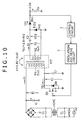
- Fig. 10 illustrates one configuration example of a switching power supply circuit including a single-ended voltage resonant converter.
- a voltage from a commercial alternating-current power supply AC is rectified and smoothed by a rectifying and smoothing circuit formed of a bridge rectifier circuit Di and a smoothing capacitor Ci, to thereby produce a rectified and smoothed voltage Ei as the voltage across the smoothing capacitor Ci.
- the lines from the commercial power supply AC are provided with a noise filter that includes a pair of common mode choke coils CMC and two across-line capacitors CL, and removes common mode noise.
- the rectified and smoothed voltage Ei is input to the voltage resonant converter as a DC input voltage.
- the voltage resonant converter has a single-ended configuration including a one-transistor switching element Q1 as described above.
- the voltage resonant converter in this circuit is separately excited.
- the switching element Q1 formed of a MOS-FET is switch-driven by an oscillation and drive circuit 2.
- a body diode DD of the MOS-FET is connected in parallel to the switching element Q1.
- a primary-side parallel resonant capacitor Cr is connected in parallel to the channel between the drain and source of the switching element Q1.
- the primary-side parallel resonant capacitor Cr and the leakage inductance L1 of a primary winding N1 in an isolation converter transformer PIT form a primary-side parallel resonant circuit (voltage resonant circuit).
- This primary-side parallel resonant circuit offers voltage resonant operation as the switching operation of the switching element Q1.
- the oscillation and drive circuit 2 applies a gate voltage as a drive signal to the gate of the switching element Q1.
- the switching element Q1 implements switching operation with the switching frequency dependent upon the cycle of the drive signal.
- the isolation converter transformer PIT transmits switching outputs from the switching element Q1 to the secondary side.
- the isolation converter transformer PIT is constructed of an EE-shaped core that is formed by combining E-shaped cores composed of a ferrite material for example. Furthermore, the primary winding N 1 and a secondary winding N2 are wound around the center magnetic leg of the EE-shaped core, with the winding part being divided into the primary side and secondary side.
- a gap with a length of about 1.0 mm is provided in the center leg of the EE-shaped core in the isolation converter transformer PIT, so that a coupling coefficient k of about 0.80 to 0.85 is obtained between the primary side and the secondary side.
- the coupling coefficient k has such a value, the coupling degree between the primary and secondary sides may be regarded as loose coupling, and thus it is difficult to obtain the saturation state.
- the value of the coupling coefficient k is a factor in setting the leakage inductance (L1).
- One end of the primary winding N1 in the isolation converter transformer PIT is interposed between the switching element Q1 and the positive electrode of the smoothing capacitor Ci. Thus, the transmission of the switching output from the switching element Q1 is allowed.
- the secondary winding N2 of the isolation converter transformer PIT an alternating voltage induced by the primary winding N1 is generated.
- a secondary-side series resonant capacitor C2 is connected in series to one end of the secondary winding N2, and therefore the leakage inductance L2 of the secondary winding N2 and the capacitance of the secondary-side series resonant capacitor C2 form a secondary-side series resonant circuit (current resonant circuit).
- rectifier diodes Do1 and Do2 and a smoothing capacitor Co are connected to this secondary-side series resonant circuit as shown in the drawing, so that a voltage-doubler half-wave rectifier circuit is formed.
- This voltage-doubler half-wave rectifier circuit produces, as the voltage across the smoothing capacitor Co, a secondary-side DC output voltage Eo with the level twice that of an alternating voltage V2 induced in the secondary winding N2.
- the secondary-side DC output voltage Eo is supplied to a load, and is input to a control circuit 1 as a detected voltage for constant-voltage control.
- the control circuit 1 detects the level of the secondary-side DC output voltage Eo input as a detected voltage, and then inputs the obtained detection output to the oscillation and drive circuit 2.
- the oscillation and drive circuit 2 outputs a drive signal of which frequency and so on are varied depending on the level of the secondary-side DC output voltage Eo indicated by the detection output, to thereby control the switching operation of the switching element Q1 so that the secondary-side DC output voltage Eo is kept constant at a predetermined level.
- stabilization control of the secondary-side DC output voltage Eo is achieved.
- Figs. 11A to 11C and 12 show experimental results on the power supply circuit in Fig. 10.
- major parts in the power supply circuit of Fig. 10 were designed to have the following parameters.
- the core of the isolation converter transformer PIT employed an EER-35 core, and a gap in the center leg thereof was designed to have a gap length of 1 mm.
- the numbers of turns of the primary winding N1 and the secondary winding N2 were set to 39 T and 23 T, respectively.
- the induction voltage level per one turn (T) in the secondary winding N2 was set to 3 V/T.
- the coupling coefficient k of the isolation converter transformer PIT was set to 0.81.
- the capacitance of the primary-side parallel resonant capacitor Cr was set to 3900 pF.
- the capacitance of the secondary-side series resonant capacitor C2 was set to 0.1 ⁇ F. Accordingly, the resonant frequency fo1 of the primary-side parallel resonant circuit was set to 230 kHz, and the resonant frequency fo2 of the secondary-side series resonant circuit was set to 82 kHz. Therefore, the relative relationship between the resonant frequencies fo1 and fo2 can be represented as fo1 ⁇ 2.8 ⁇ fo2.
- the rated level of the secondary-side DC output voltage Eo was 135 V.
- the allowable load power range was from the maximum load power Pomax of 200 W to the minimum load power Pomin of 0 W.
- Figs. 11A to 11C are waveform diagrams showing the operation of the major parts in the power supply circuit in Fig. 10, with reflecting the corresponding switching cycle of the switching element Q1.
- Fig. 11A shows a voltage V1, a switching current IQ1, a primary winding current I1, a secondary winding current I2, and secondary-side rectified currents ID1 and ID2, when the load power is the maximum load power Pomax of 200 W and the AC input voltage VAC of 100 V.
- Fig. 11B shows the voltage V1, the switching current IQ1, the primary winding current I1, and the secondary winding current I2, when the load power is intermediate load power Po of 120 W.
- Fig. 11C shows the voltage V1 and the switching current IQ1 when the load power is the minimum load power Pomin of 0 W.
- the voltage V1 is the voltage obtained across the switching element Q1, and has a waveform like those in Figs. 11A to 11C. Specifically, the voltage level is at zero level during the period TON when the switching element Q1 is in the on-state, while a sinusoidal resonant pulse is obtained during the period TOFF when it is in the off state. This resonant pulse waveform of the voltage V1 indicates that the operation of the primary-side switching converter is voltage resonant operation.
- the switching current IQ1 is the current flowing through the switching element Q1 (and the body diode DD).
- the switching current IQ1 flows with the illustrated waveforms during the period TON, while it is at zero level during the period TOFF.
- the primary winding current I1 flowing through the primary winding N1 is the current resulting from the synthesis between the current flowing as the switching current IQ1 during the period TON and the current flowing to the primary-side parallel resonant capacitor Cr during the period TOFF.
- the rectified currents ID1 and ID2, shown only in Fig. 11A, flowing through the rectifier diodes Do1 and Do2 as the operation of the secondary-side rectifier circuit have sinusoidal waveforms like the illustrated ones.
- the waveform of the rectified current ID1 indicates the resonant operation of the secondary-side series resonant circuit more dominantly than the waveform of the rectified current ID2.
- the secondary winding current I2 flowing through the secondary winding N2 has a waveform resulting from the synthesis between the waveforms of the rectified currents ID 1 and ID2.
- Fig. 12 shows, as functions of the load, the switching frequency fs, the lengths of ON and OFF periods TON and TOFF of the switching element Q1, and the AC to DC power conversion efficiency ( ⁇ AC ⁇ DC) of the power supply circuit shown in Fig. 10.
- the switching frequency fs, the period TON, and the period TOFF in Fig. 12 indicate the switching operation of the power supply circuit in Fig. 10 as the characteristic of constant-voltage control against load variation.
- the switching frequency fs is almost constant against the load variation.
- the periods TON and TOFF show linear changes having opposite tendencies as shown in Fig. 12.
- These characteristics show that the switching operation is controlled against the variation of the secondary-side DC output voltage Eo such that the time ratio between the ON and OFF periods is changed with the switching frequency (switching cycle) being kept almost constant.
- This control can be regarded as pulse width modulation (PWM) control, in which the lengths of the ON and OFF periods within one switching cycle are changed.
- PWM control allows the power supply circuit in Fig. 10 to stabilize the secondary-side DC output voltage Eo.
- Fig. 13 schematically shows the constant-voltage control characteristic of the power supply circuit shown in Fig. 10, based on the relationship between the switching frequency fs (kHz) and the secondary-side DC output voltage Eo.
- the power supply circuit shown in Fig. 10 includes a primary-side parallel resonant circuit and a secondary-side series resonant circuit, and therefore has two resonant impedance characteristics in a complex manner: the resonant impedance characteristic corresponding to the resonant frequency fo1 of the primary-side parallel resonant circuit, and that corresponding to the resonant frequency fo2 of the secondary-side series resonant circuit. Since the power supply circuit in Fig. 10 has the frequency relationship fo1 ⁇ 2.8 ⁇ fo2, the secondary-side series resonant frequency fo2 is lower than the primary-side parallel resonant frequency fo1 also as shown in Fig. 13.
- Characteristic curves in Fig. 13 show a constant-voltage control characteristic that depends on control of the switching frequency fs and is assumed based on these resonant frequencies and under the condition of a certain constant AC input voltage VAC.
- Characteristic curves A and B correspond to the maximum load power Pomax and the minimum load power Pomin, respectively, and indicate the constant-voltage control characteristic in relation to the resonant impedance corresponding to the resonant frequency fo1 of the primary-side parallel resonant circuit.
- Characteristic curves C and D correspond to the maximum load power Pomax and the minimum load power Pomin, respectively, and indicate the constant-voltage control characteristic in relation to the resonant impedance corresponding to the resonant frequency fo2 of the secondary-side series resonant circuit.
- constant-voltage control is intended so that the output voltage is kept at the voltage tg that is the rated level of the secondary-side DC output voltage Eo
- the variation range of the switching frequency fs required for the constant-voltage control (requisite control range) can be expressed by the section indicated by ⁇ fs.
- the requisite control range ⁇ fs shown in Fig. 13 is from the frequency offering the voltage level tg on Characteristic curve C, corresponding to the resonant frequency fo2 of the secondary-side series resonant circuit and the maximum load power Pomax, to that on Characteristic curve B, corresponding to the resonant frequency fo1 of the primary-side parallel resonant circuit and the minimum load power Pomin.
- the range ⁇ fs includes the frequency offering the voltage level tg on Characteristic curve D, corresponding to the resonant frequency fo2 of the secondary-side series resonant circuit and the minimum load power Pomin, and that on Characteristic curve A, corresponding to the resonant frequency fo1 of the primary-side parallel resonant circuit and the maximum load power Pomax.
- the power supply circuit in Fig. 10 implements switching drive control based on PWM control in which the time ratio of the periods TON/TOFF in one switching cycle is changed with the switching frequency fs being kept almost constant.
- the implementation of the PWM control is indicated also by Figs. 11A to 11C, in which the widths of the periods TOFF and TON change depending on the load power while the length of one switching cycle (TOFF+TON) is almost constant irrespective of the load power.
- This operation is due to such a resonant impedance characteristic of the power supply circuit against load variation that transition is implemented, in the narrow switching frequency range ( ⁇ fs), between the state where the resonant impedance corresponding to the resonant frequency fo1 of the primary-side parallel resonant circuit (capacitive impedance) is dominant, and the state where the resonant impedance corresponding to the resonant frequency fo2 of the secondary-side series resonant circuit (inductive impedance) is dominant.
- ⁇ fs narrow switching frequency range
- the power supply circuit in Fig. 10 involves the following problems.
- the switching current IQ1 when the load power is the maximum load power Pomax operates as follows. Specifically, the switching current IQ1 is at zero level until the end of the period TOFF, which is the turn on timing of the switching element Q1. When the period TON starts, initially a current of the negative polarity flows through the body diode DD, and then the polarity is inverted and the switching current IQ1 flows between the drain and source of the switching element Q1. This operation indicates the state where zero voltage switching (ZVS) is adequately carried out.
- ZVS zero voltage switching
- the switching current IQ1 when the load power is the intermediate load power Po of 120 W shows a waveform in which a noise current flows at timing immediately before the end of the period TOFF, which is the turn-on timing of the switching element Q1.
- This waveform indicates abnormal operation in which ZVS is not implemented adequately.
- a voltage resonant converter including a secondary-side series resonant circuit as shown in Fig. 10 involves abnormal operation in which ZVS is not implemented adequately when the load is an intermediate load. It has been confirmed that, in an actual power supply circuit of Fig. 10, such abnormal operation arises in the load variation range indicated by the section A in Fig. 12 for example.
- a voltage resonant converter including a secondary-side series resonant circuit originally has a tendency to have a characteristic of keeping high efficiency favorably against load variation as described above.
- a corresponding peak current flows at the turn-on timing of the switching element Q1.
- This noise current causes an increase of switching loss, which is a factor in a decrease of the power conversion efficiency.
- an embodiment of the present invention provides a switching power supply circuit having the following configuration.
- the power supply circuit includes a switching element that implements switching for a DC voltage to thereby convert the DC voltage into an AC voltage, a converter transformer in which the AC voltage is input to a primary winding so that an AC voltage is generated in a secondary winding, a secondary-side rectifying and smoothing circuit that includes a secondary-side rectifier element and a secondary-side smoothing capacitor for rectifying and smoothing the AC voltage generated in the secondary winding to thereby produce an output DC voltage, and a switching element control unit that controls the switching element based on the output DC voltage.
- the DC voltage is supplied to one winding end of the primary winding in the converter transformer via a choke coil, and the switching element is connected to the other winding end of the primary winding in the converter transformer so that the AC voltage is generated.
- a series resonant capacitor is coupled to the connecting node between the one winding end of the primary winding in the converter transformer and the choke coil, so that a first series resonant circuit of which resonant frequency is dominated by the leakage inductance arising in the primary winding in the converter transformer and the series resonant capacitor is formed, and so that a second series resonant circuit of which resonant frequency is dominated by the inductance of the choke coil and the series resonant capacitor is formed, and the resonant frequency of the first series resonant circuit and the resonant frequency of the second series resonant circuit are set to be substantially equal to each other.
- a parallel resonant circuit of which resonant frequency is dominated by a primary-side parallel resonant capacitor connected in parallel to the switching element, the inductance of the choke coil and the leakage inductance arising in the primary winding is formed, and the resonant frequency of the parallel resonant circuit is set higher than the resonant frequency of the first series resonant circuit and the resonant frequency of the second series resonant circuit.
- the secondary winding includes a first secondary winding and a second secondary winding so that currents in the directions of the opposite polarities are extracted from the first and second secondary windings through first and second rectifier diodes, respectively, included in the secondary-side rectifier element, and the ratio of the number of turns of the first secondary winding to the number of turns of the second secondary winding is defined so that the magnitudes of the currents in the directions of the opposite polarities are substantially equal to each other.
- the power supply circuit with the above-described configuration includes a primary-side rectifying and smoothing circuit that includes a primary-side rectifier element and a primary-side smoothing capacitor for producing a DC voltage, a switching element that implements switching for the DC voltage to thereby convert the DC voltage into an AC voltage; a converter transformer in which the AC voltage is input to a primary winding so that an AC voltage is generated in a secondary winding, a secondary-side rectifying and smoothing circuit that includes a secondary-side rectifier element and a secondary-side smoothing capacitor for rectifying and smoothing the AC voltage generated in the secondary winding to thereby produce an output DC voltage, and a switching element control unit that controls the switching element based on the output DC voltage.
- the power supply circuit has the following features.
- the DC voltage is supplied to one winding end of the primary winding in the converter transformer via a choke coil, and the switching element is connected to the other winding end of the primary winding in the converter transformer so that the AC voltage is generated.
- the operation of the power supply circuit is close to so-called class-E operation, and the current supplied from a smoothing and rectifying circuit has a ripple waveform close to a DC component.
- a series resonant capacitor is coupled to the connecting node between the one winding end of the primary winding in the converter transformer and the choke coil, so that a first series resonant circuit of which resonant frequency is dominated by the leakage inductance arising in the primary winding in the converter transformer and the series resonant capacitor is formed, and so that a second series resonant circuit of which resonant frequency is dominated by the inductance of the choke coil and the series resonant capacitor is formed, and the resonant frequency of the first series resonant circuit and the resonant frequency of the second series resonant circuit are set to be substantially equal to each other.
- a parallel resonant circuit of which resonant frequency is dominated by a primary-side parallel resonant capacitor connected in parallel to the switching element, the inductance of the choke coil and the leakage inductance arising in the primary winding is formed, and the resonant frequency of the parallel resonant circuit is set higher than the resonant frequency of the first series resonant circuit and the resonant frequency of the second series resonant circuit.
- so-called current and voltage resonant converters are constructed, so that the frequency of the AC voltage can be controlled within a small range for control of the output DC voltage.
- the secondary winding includes a first secondary winding and a second secondary winding so that currents in the directions of the opposite polarities are extracted from the first and second secondary windings through first and second rectifier diodes, respectively, included in the secondary-side rectifier element, and the ratio of the number of turns of the first secondary winding to the number of turns of the second secondary winding is defined so that the magnitudes of the currents in the directions of the opposite polarities are substantially equal to each other.
- the currents can be extracted from the secondary winding effectively.
- abnormal operation in which zero voltage switching (ZVS) operation is not achieved in an intermediate load condition range is eliminated from a switching power supply circuit including a parallel resonant circuit on its primary side.
- Fig. 8 illustrates the basic configuration of a class-E switching converter.
- the class-E switching converter in this drawing has a configuration as a DC-AC inverter that operates in a class-E resonant mode.
- This class-E switching converter includes a one-transistor switching element Q1.
- the switching electrode Q1 is a MOS-FET in this converter.
- a body diode DD is connected in parallel to the channel between the drain and source of the MOS-FET switching element Q1.
- the forward direction of the body diode DD is the same as the direction from the source to the drain of the switching element Q1.
- a primary-side parallel resonant capacitor Cr is connected in parallel to the channel between the drain and source of the switching element Q1.
- the drain of the switching element Q1 is connected in series to a choke coil L10, and is coupled via the choke coil L10 to the positive electrode of a DC input power supply Ein.
- the source of the switching element Q1 is connected to the negative electrode of the DC input power supply Ein.
- the drain of the switching element Q1 is connected to one end of a choke coil L11.
- the other end of the choke coil L11 is connected in series to a series resonant capacitor C11.
- An impedance Z as a load is interposed between the series resonant capacitor C11 and the negative electrode of the DC input power supply Ein.
- Specific examples of the impedance Z include a piezoelectric transformer and a high-frequency-compatible fluorescent lamp.
- the class-E switching converter with this configuration can be regarded as one form of a complex resonant converter that includes a parallel resonant circuit formed of the inductance of the choke coil L10 and the capacitance of the primary-side parallel resonant capacitor Cr, and a series resonant circuit formed of the inductance of the choke coil L11 and the capacitance of the series resonant capacitor C11.
- the class-E switching converter since the class-E switching converter includes only one switching element, it can be regarded as equivalent to a single-ended voltage resonant converter.
- Fig. 9 shows the operation of major parts in the class-E switching converter shown in Fig. 8.
- a switching voltage V1 is the voltage obtained across the switching element Q1, and has a waveform like that in Fig. 9. Specifically, the voltage level is at zero level during the period TON when the switching element Q1 is in the on-state, while a sinusoidal pulse is obtained during the period TOFF when it is in the off-state.
- This switching pulse waveform is due to the resonant operation (voltage resonant operation) of the above-described parallel resonant circuit.
- a switching current IQ1 is the current flowing through the switching element Q1 (and the body diode DD).
- the switching current IQ1 is at zero level.
- the switching current IQ1 has a certain waveform like illustrated one. Specifically, during a certain period from the start of the period TON, the switching current IQ1 initially flows through the body diode DD, and thus has the negative polarity. Subsequently, the switching current IQ1 is inverted to the positive polarity, and thus flows from the drain to the source of the switching element Q1.
- a current I2 flowing through the series resonant circuit as an output of the class-E switching converter results from the synthesis between the switching current IQ1 flowing through the switching element Q1 (and the body diode DD) and the current flowing to the primary-side parallel resonant capacitor Cr, and has a waveform including sinusoidal wave components.
- the waveforms of the switching current IQ1 and the switching voltage V1 indicate that ZVS operation is achieved at the turn-off timing of the switching element Q1, and ZVS and ZCS operations are achieved at the turn-on timing thereof.
- a current II flowing from the positive electrode of the DC input power supply Ein through the choke coil L10 to the class-E switching converter has a ripple waveform with a certain average current level like the illustrated one, since the inductance of the choke coil L10 is set larger than that of the choke coil L11.
- This ripple current can be regarded as a DC current approximately.
- Fig. 1 illustrates a configuration example of a power supply circuit of a first embodiment of the present invention as a power supply circuit with a configuration based on the class-E switching converter.
- the same parts in Fig. 1 as those in Fig. 8 are given the same numerals and the description therefor will be omitted.
- one end of a choke coil winding N10 is connected to the positive electrode of a smoothing capacitor Ci while the other end of the choke coil winding N10 is connected to one end of a primary winding N1.
- one electrode of a primary-side series resonant capacitor C11 is coupled to the connecting node between one end of the primary winding N1 and the other end of the choke coil winding N10.
- the other electrode of the primary-side series resonant capacitor C11 is coupled to the connecting node between one electrode of a primary-side parallel resonant capacitor Cr and the source of a switching element Q1, at the primary-side ground potential.
- the primary-side series resonant capacitor C 11 is connected in series to the primary winding N1.
- the primary-side parallel resonant capacitor Cr is connected in parallel to the channel between the source and drain of the switching element Q 1.
- the thus provided choke coil winding N10 is equivalent to the winding as the choke coil L10 in Fig. 8.
- the choke coil winding N10 is wound around a core having predetermined shape and size, and thus constructs a component element as a choke coil PCC.
- a primary-side parallel resonant circuit is formed of the capacitance of the primary-side parallel resonant capacitor Cr and the synthetic inductance arising from the inductance L10 of the choke coil winding N10 (choke coil PCC) and the leakage inductance L1 of the primary winding N1.
- the power supply circuit includes a first primary-side series resonant circuit formed of the capacitance of the primary-side series resonant capacitor C11 and the leakage inductance L1 of the primary winding N1, based on the series connection between the primary-side series resonant capacitor C11 and the primary winding N1.
- the power supply circuit includes a second primary-side series resonant circuit formed of the inductance L10 of the choke coil winding N10 and the capacitance of the primary-side series resonant capacitor C11, based on the series connection between the choke coil winding N10 and the primary-side series resonant capacitor C 11.
- charging/discharging currents flow to and from the primary-side parallel resonant capacitor Cr during the periods when the switching element Q1 is in the off-state, due to the voltage resonant operation of the above-described primary-side parallel resonant circuit.
- These charging/discharging currents generate a resonant pulse voltage with substantially sinusoidal half waves as the voltage across the primary-side parallel resonant capacitor Cr.
- the primary winding N1 is provided in the primary-side parallel resonant circuit, such operation arises in the primary winding N1 that the resonant pulse voltage is superimposed on an alternating voltage arising in response to a switching current.
- the first primary-side series resonant circuit implements resonant operation so that a resonant current flows through the path of the primary-side series resonant capacitor C11, the primary winding N1, and the switching element Q1.
- the second primary-side series resonant circuit implements resonant operation so that a resonant current flows through the path of the primary-side series resonant capacitor C11, the choke coil winding N10, and the smoothing capacitor Ci.
- the series resonant current that should flow through the primary winding N1 shunt so as to flow also through the choke coil winding N10 for example.
- both the current paths can be regarded as being parallel to each other with the primary-side series resonant capacitor C11 being common to both the paths.
- the inductance (L1) obtained across the primary winding N1 and the inductance (L10) obtained across the choke coil winding N10 can be equalized to each other, which allows reduction of the size of the choke coil PCC provided with the choke coil winding N10.
- the resonant frequency of the first primary-side series resonant circuit is dominated by the value of the leakage inductance (L1) arising in the primary winding N1 and the capacitance value of the primary-side series resonant capacitor C11, while the resonant frequency of the second primary-side series resonant circuit is dominated by the value of the inductance (L10) obtained in the choke coil winding N10 and the capacitance value of the primary-side series resonant capacitor C11.
- the resonant frequency of the first primary-side series resonant circuit and the resonant frequency of the second primary-side series resonant circuit can be equalized to each other.
- a favorable control characteristic can be achieved even when the variable range of the frequency of the AC signal supplied from the oscillation and drive circuit 2 serving as part of the control unit to the switching element Q1 is small.
- the expression that the resonant frequency is "dominated" indicates the fact that the value of the resonant frequency of the first primary-side series resonant circuit greatly depends upon the value of the leakage inductance (L1) arising in the primary winding N 1 and the capacitance value of the primary-side series resonant capacitor C11, and the value of the resonant frequency of the second primary-side series resonant circuit greatly depends upon the value of the inductance (L10) obtained in the choke coil winding N10 and the capacitance value of the primary-side series resonant capacitor C11.
- the smoothing capacitor Ci also forms part of the second primary-side series resonant circuit, the capacitance value of the smoothing capacitor Ci does not dominate the resonant frequency since it is greatly larger than the capacitance value of the primary-side series resonant capacitor C11.
- the secondary winding is provided with a center tap, and the setting is defined so that the magnitudes of the currents flowing through a rectifier diode Do1 and a rectifier diode Do2 are equal to each other. If the setting is made so that the magnitudes of the currents flowing through the rectifier diode Do1 and the rectifier diode Do2 are equal to each other, the load current uniformly flows over the entire cycles, which can enhance the efficiency of the switching power supply circuit.
- a secondary-side partial voltage resonant capacitor C3 is provided. Therefore, partial voltage resonance arises, and thus the occurrence of switching loss at the changeover points between the on- and off-states of the rectifier diodes Do1 and Do2 can be prevented, which can further enhance the efficiency of the switching power supply circuit.
- Fig. 5 illustrates a structural example of an isolation converter transformer PIT included in the power supply circuit of Fig. 1 with the above-described configuration.
- the isolation converter transformer PIT includes an EE-core (EE-shaped core) formed by combining E-shaped cores CR1 and CR2 made of a ferrite material in such a manner that their magnetic legs face each other.
- EE-core EE-shaped core
- a bobbin B is provided that is formed of resin or the like and has such a divided shape that winding parts on the primary side and secondary side are independent of each other.
- the primary winding N1 is wound around one winding part of the bobbin B.
- the secondary winding N2 and a secondary winding N2' are wound around the other winding part.
- the bobbin B around which the primary-side and secondary-side windings have been thus wound is fitted to the EE-shaped core (CR1, CR2), which results in the state in which the primary-side and secondary-side windings on different winding regions are wound around the center leg of the EE-shaped core. In this manner, the entire structure of the isolation converter transformer PIT is completed.
- a gap G having a gap length of e.g. about 1.6 mm or more is formed as shown in the drawing.
- a loose coupling state in which a coupling coefficient k is e.g. about 0.75 is obtained. That is, the degree of loose coupling is higher in the isolation converter transformer PIT in Fig. 1, compared with that in the power supply circuit shown in Fig. 10 as a conventional technique.
- the gap G can be formed by setting the center legs of the E-shaped cores CR1 and CR2 to be shorter than the respective two outer legs thereof.
- EER-35 is used as the core member, and the length of the gap G is set to 2.2 mm.
- the numbers of turns of the primary winding N1, the secondary winding N2, and the secondary winding N2' are set to 50 T, 35 T, and 45 T, respectively. Furthermore, the coupling coefficient k between the primary and secondary sides of the isolation converter transformer PIT itself is set to a value smaller than 0.7 for example.
- the choke coil PCC can also be constructed by providing a winding around an EE-shaped core with predetermined shape and size.
- ER-28 is used as the core member
- the length of the gap G is set to 1.2 mm
- the number of turns of the choke coil winding N10 is set to 45 T.
- 303 ⁇ H is obtained as the inductance value of the inductor L10.
- the primary-side parallel resonant frequency fo1 was set to 85.8 kHz.
- the primary-side series resonant frequency fo2 dependent upon the primary-side series resonant capacitor C11 and the inductor L1 was set to 54.8 kHz.
- the primary-side series resonant frequency fo2' dependent upon the primary-side series resonant capacitor C11 and the inductor L10 was set to 55.7 kHz. That is, two primary-side series resonant frequencies fo2 and fo2' were substantially equalized to each other, and were set lower than the primary-side parallel resonant frequency fo1.
- the allowable load power range was from the maximum load power Pomax of 300 W to the minimum load power Pomin of 0 W (no load).
- the rated level of the secondary-side DC output voltage Eo was 175 V.
- Fig. 2A shows a switching voltage V1, a switching current IQ1, a primary winding voltage V2, a choke coil current I1, a primary winding current I2, a secondary-side alternating voltage V3, and a secondary winding current I3 under the condition of the maximum load power Pomax of 300 W and the AC input voltage VAC of 100 V.
- Fig. 2B shows the switching voltage V1, the switching current IQ1, the primary winding voltage V2, the choke coil current I1, the primary winding current 12, the secondary-side alternating voltage V3, and the secondary winding current I3 under the condition of the minimum load power Pomin of 0 W and the AC input voltage VAC of 100 V.
- the input current I1 is the current that flows from the smoothing capacitor Ci to the primary-side switching converter.
- the input current I1 flows via the synthetic inductance arising from the inductance L10 of the choke coil winding N10 and the leakage inductance L1 of the primary winding N1.
- the current flowing from the smoothing capacitor Ci to the switching converter is a ripple current.
- the switching element Q1 is provided with the voltage across the smoothing capacitor Ci (Ei) as a DC input voltage, and implements switching operation.
- the switching voltage V is the voltage between the drain and source of the switching element Q1.
- the switching current IQ1 is the current that flows through the switching element Q1 (and the body diode DD) from the drain side thereof.
- Each switching cycle is divided into the period TON during which the switching element Q1 should be in the on-state, and the period TOFF during which it should be in the off-state.
- the switching voltage V1 has a waveform in which the voltage is at zero level during the period TON and is a resonant pulse during the period TOFF. This voltage resonant pulse of the switching voltage V1 is obtained as a pulse having a sinusoidal resonant waveform due to the resonant operation of the primary-side parallel resonant circuit.
- the switching current IQ1 is at zero level during the period TOFF.
- the period TOFF ends and the period TON starts, i.e., at the turn-on timing of the switching element Q1
- the switching current IQ1 flows through the body diode DD and therefore has the negative polarity waveform.
- the flow direction is inverted so that the switching current IQ1 flows from the drain to the source, and therefore the switching current IQ1 has the positive polarity waveform.
- the primary winding current 12 is the current that flows through the primary winding N1 in response to the switching operation of the switching element Q1, and approximately has the waveform arising from the synthesis of the switching current IQ1 and a capacitor current Icr. Due to the ON/OFF operation of the switching element Q1, a resonant pulse voltage, which is the switching voltage V1 in the period TOFF, is applied to the series circuit of the primary winding N1 and the primary-side series resonant capacitor C11, which form the first primary-side series resonant circuit. Thus, the primary-side series resonant circuit implements resonant operation, and the primary winding current 12 has an alternating waveform based on sinusoidal components and dependent upon the switching cycle.
- the primary winding voltage V2 is the voltage across the primary winding N1. This primary winding voltage V2 also has an alternating waveform based on a sinewave and dependent upon the switching cycle as shown in the waveform diagrams.
- the primary winding current 12 flows as the capacitor current Icr to the primary-side parallel resonant capacitor Cr with the positive polarity, and thus operation of charging the primary-side parallel resonant capacitor Cr is started.
- the switching voltage V1 starts to rise from zero levels with a sinusoidal waveform, i.e., a voltage resonant pulse rises up.
- the state of the primary-side parallel resonant capacitor Cr changes from the charging state to the discharging state, which causes the voltage resonant pulse to fall down from its peak level with the sinusoidal waveform.
- the period TON during which the switching element Q1 (and the body diode DD) is in the on-state is started.
- the cycle sequence reaches the period TON, initially the body diode DD conducts, so that the primary winding current 12 with the negative polarity flows.
- the switching voltage V1 is at zero levels.
- the switching element Q1 is turned on and thus the positive primary winding current 12 flows therethrough.
- the switching current IQ1 Since the primary winding current I2 flows through the switching element Q1 (and the body diode DD) during the period TON in this manner, the switching current IQ1 has a waveform like the illustrated one.
- the above-described operation indicates that, at the turn-on and turn-off timings of the switching element Q1, ZVS operation due to the primary-side parallel resonant circuit and ZCS operation due to the primary-side series resonant circuit are achieved.
- the secondary-side alternating voltage V3 indicates the operation of the secondary-side rectifier circuit.
- the secondary-side alternating voltage V3 is the voltage across the connection circuit of the secondary windings N2 and N2' and the secondary-side partial voltage resonant capacitor C3, and is input to the secondary-side rectifier circuit. In the period of each half cycle of the voltage V3, a forward voltage is applied to either one of the rectifier diodes Do1 and Do2 in turn, which leads to the alternate conduction of the rectifier diodes Do1 and Do2. Thus, the secondary-side alternating voltage V3 is clamped at the level having the absolute value equal to the secondary-side DC output voltage Eo, in the conducting periods of the rectifier diodes Do1 and Do2.
- the isolation converter transformer PIT cannot transmit a DC component
- the zero level of the voltage arising in the secondary windings N2 and N2' is defined so that the time integration value of the positive component of the voltage and that of the negative component of the voltage are equal to each other. Therefore, if the numbers of turns of the secondary windings N2 and N2' are the same, the magnitudes of the currents flowing through the rectifier diodes Do1 and Do2 are different from each other.
- the numbers of turns of the secondary windings N2 and N2' are set to different numbers of 35 T and 45 T, respectively.
- the magnitudes of the currents flowing through the rectifier diodes Do1 and Do2 are equalized to each other.
- the provision of the partial voltage resonant capacitor C3 allows the currents at the voltage changeover points to flow to the partial voltage resonant capacitor C3 to thereby improve the efficiency.
- the capacitance value of the partial voltage resonant capacitor C3 was in the range of about 200 to 470 pF, a favorable efficiency improvement effect could be achieved.
- the AC to DC power conversion efficiency ( ⁇ AC ⁇ DC) of the modified class-E switching operation multiple resonant converter of the present embodiment shown in Fig. 1 was 91.3% when the load power was the maximum load power Pomax of 300 W, and was 91.7% when it was 100 W as shown in Fig. 3 under the condition of the AC input voltage VAC of 100 V.
- Fig. 4 shows, as functions of the input AC voltage, the variation characteristic when the load power was the maximum load power Pomax of 300 W, an experimental result that the variable range ⁇ fs of the switching frequency fs was 11.0 kHz was obtained.
- the current that flows from the smoothing capacitor Ci into the switching converter passes through the primary winding N1 in the isolation converter transformer PIT, and then reaches the switching element Q1 and the primary-side parallel resonant capacitor Cr.
- This current flowing from the smoothing capacitor Ci to the switching converter is the primary winding current I1, and has a comparatively high frequency dependent upon the switching cycle. That is, charging and discharging currents flow to and from the smoothing capacitor Ci with a frequency higher than the frequency of the commercial AC voltage.
- An aluminum electrolytic capacitor is often employed for a component element as the smoothing capacitor Ci because of the need for the capacitor Ci to have a high breakdown voltage, and so on.
- the aluminum electrolytic capacitor has an increased tendency to suffer from lowering of the electrostatic capacitance and an increase of the tangent of the loss angle when being operated at a high frequency, compared with other kinds of capacitors. Therefore, there is a need to choose, as the aluminum electrolytic capacitor for the smoothing capacitor Ci, a special product of which equivalent series resistance (ESR) is low, and of which allowable ripple current is large.
- ESR equivalent series resistance
- the capacitance needs to be about 1000 ⁇ F in order to address the maximum load power Pomax of 300 W, which is the same as the maximum load power in the present embodiment.
- An aluminum electrolytic capacitor compatible with these requirements is more expensive than general-purpose aluminum electrolytic capacitors, and the increase of the capacitance leads to a rise of the component price. Therefore, use of such a special capacitor is disadvantageous in terms of costs.
- the current that flows from the smoothing capacitor Ci into the switching converter passes through the series connection of the choke coil winding N10 and the primary winding N1, and then reaches the switching element Q1. Therefore, the current flowing from the smoothing capacitor Ci to the switching converter becomes a DC current as indicated by the input current I1 of Fig. 2A. Since the current flowing from the smoothing capacitor Ci to the switching converter is a DC current, the present embodiment does not involve the above-described problems of lowering of the electrostatic capacitance and an increase of the tangent of the loss angle. Furthermore, along with this, a ripple with the cycle of the commercial AC supply voltage in the DC input voltage Ei is also reduced.
- This ripple is 5 Vp-p in the power supply circuit in Fig. 1, in contrast to e.g. the power supply circuit of Fig. 10, in which the ripple is 7.5 Vp-p.
- a general-purpose aluminum electrolytic capacitor can be chosen as the smoothing capacitor Ci.
- the capacitance of the component as the smoothing capacitor Ci can be lowered compared with in the circuit of Fig. 10, since the ripple voltage is small.
- a capacitance of 680 ⁇ F is allowed in an actual power supply circuit of Fig. 1.
- the present embodiment can achieve cost reduction of the smoothing capacitor Ci.
- the waveform of the input current I1 is a sinusoidal waveform. This also contributes to achievement of the high-frequency noise reduction effect.
- the present embodiment eliminates the occurrence of abnormal operation associated with an intermediate load, to thereby allow adequate ZVS operation also as described above.
- the switching element Q1 is turned on and the positive switching current IQ1 flows between the source and drain thereof before the original turn-on timing of the switching element Q1 (the start timing of the period TON), as shown in Fig. 11B.
- Such operation of the switching current IQ1 increases switching loss.
- the present embodiment prevents the occurrence of the abnormal operation of the switching current IQ1, and thus eliminates the increase of switching loss. This feature is also one factor in the enhancement of the power conversion efficiency.
- the switching current IQ1 of Fig. 2A has a waveform in which current peaks appear at timings before the end timings of the period TON.
- the waveform of the switching current IQ1 shown in Fig. 2A indicates that the level of the switching current IQ1 at the turn-off timing of the switching element Q1 is suppressed. If the level of the switching current IQ1 at the turn-off timing is suppressed, the switching loss at the turn-off timing is correspondingly reduced, which enhances the power conversion efficiency.
- Such a waveform of the switching current IQ1 is due to the class-E switching operation of the primary-side switching converter.
- the series resonant current that should flow in the primary side flows with being divided to the primary winding N1 and the choke coil winding N10. This current division decreases the magnitude of the primary winding current 12, and hence improves the efficiency.
- the waveform of the input current I1 is a sinusoidal waveform, which also contributes to achievement of the high-frequency noise reduction effect.
- the numbers of turns of the secondary windings N2 and N2' are made different, and thus the currents of both the positive and negative polarities generated dependent upon the polarities of magnetic flux are equalized to each other, so that an efficiency improvement is achieved.
- a secondary-side partial voltage resonant circuit is provided.
- Fig. 6 illustrates a first modification of the power supply circuit of the embodiment.
- the same parts in Fig. 6 as those in Fig. 1 are given the same numerals and the description therefor will be omitted.
- the secondary side of the power supply circuit includes a secondary winding N2 and a secondary winding N2'.
- the secondary windings N2 and N2' are connected in series to each other so that voltages arising in the respective secondary windings are added to each other.
- Secondary-side rectifier elements include rectifier diodes Do1, Do2, Do3, and Do4.
- the rectifier diodes Do1 and Do2 are connected in series to each other with the respective cathodes, which are the same-polarity ends of one polarity, being connected to each other.
- the rectifier diodes Do3 and Do4 are connected in series to each other with the respective anodes, which are the same-polarity ends of the other polarity, being connected to each other.
- Both the ends of the secondary winding arising from the series connection of the secondary windings N2 and N2' are connected to the ends of the series connection of the rectifier diodes Do1 and Do2. Both the ends of the secondary winding N2 are connected to the ends of the series connection of the rectifier diodes Do3 and Do4.
- a secondary-side smoothing capacitor Co is coupled to the connecting node between the rectifier diodes Do 1 and Do2, and to the connecting node between the rectifier diodes Do3 and Do4.
- the voltage arising in the series connection of the secondary windings N2 and N2' causes a current to flow through the rectifier diode Do1, the secondary-side smoothing capacitor Co, and the rectifier diode Do4. Furthermore, due to magnetic flux in the other direction, the voltage arising in the secondary winding N2 causes a current to flow through the rectifier diode Do3, the secondary-side smoothing capacitor Co, and the rectifier diode Do2.
- the ratio of the number of turns of the secondary winding N2 to that of the secondary winding N2' is defined so that the magnitudes of the currents flowing in both the directions are equalized to each other.
- the period TON during which the switching element Q1 (and the body diode DD) is in the on-state is started.
- the cycle sequence reaches the period TON, initially the body diode DD conducts, so that the primary winding current I2 with the negative polarity flows.
- the switching voltage V1 is at zero level.
- the switching element Q1 is turned on and thus the positive primary winding current I2 flows therethrough.
- the switching current IQ1 Since the primary winding current I2 flows through the switching element Q1 (and the body diode DD) during the period TON in this manner, the switching current IQ1 has a waveform like the illustrated one.
- the above-described operation indicates that, at the turn-on and turn-off timings of the switching element Q1, ZVS operation due to the primary-side parallel resonant circuit and ZCS operation due to the primary-side series resonant circuit are achieved.
- the secondary-side alternating voltage V3 indicates the operation of the secondary-side rectifier circuit.
- the secondary-side alternating voltage V3 is the voltage across the connection circuit of the secondary windings N2 and N2' and the secondary-side partial voltage resonant capacitor C3, and is input to the secondary-side rectifier circuit. In the periods of half cycles of one polarity of the voltage V3, a forward voltage is applied to the rectifier diodes Do 1 and Do4, which leads to the conduction of the rectifier diodes Do1 and Do4.
- the isolation converter transformer PIT cannot transmit a DC component, if the primary-side waveform involves a distortion from a sinewave, the zero level of the secondary-side alternating voltage V3 and the voltage of the secondary winding N2 is defined so that the time integration value of the positive component of the voltages and that of the negative component of the voltages are equal to each other. Therefore, if the difference of the number of turns between the secondary windings N2 and N2' is 0 T, the magnitude of the current flowing through the rectifier diodes Do1 and Do4 is different from that of the current flowing through the rectifier diodes Do3 and Do2.
- the numbers of turns of the secondary windings N2 and N2' are set to 35 T and 10 T, respectively.
- the magnitude of the current flowing through the rectifier diodes Do1 and Do4 is equalized to that of the current flowing through the rectifier diodes Do3 and Do2.
- the provision of the partial voltage resonant capacitor C3 allows the currents at the voltage changeover points to flow to the partial voltage resonant capacitor C3 to thereby improve the efficiency.
- the AC to DC power conversion efficiency ( ⁇ AC ⁇ DC) of the modified class-E switching operation multiple resonant converter of the first modification shown in Fig. 6 was 91% when the load power was the maximum load power Pomax of 300 W, and was 93% when it was 100 W.
- an experimental result that the variable range ⁇ fs of the switching frequency fs was 10.7 kHz was obtained, and the power conversion efficiency ( ⁇ AC ⁇ DC) was enhanced as the commercial AC supply voltage increased.
- Fig. 7 illustrates a second modification of the power supply circuit of the embodiment.
- the same parts in Fig. 7 as those in Fig. 1 are given the same numerals and the description therefor will be omitted.
- an isolation converter transformer PIT includes a plurality of secondary windings: a secondary winding N2, a secondary winding N2', and a secondary winding N2".
- Secondary-side rectifier elements include a plurality of rectifier diodes Do1 to Do4 that rectify the AC voltage output from the plural secondary windings.
- Secondary-side smoothing capacitors include a secondary-side smoothing capacitor Co1 and a secondary-side smoothing capacitor Co2 to which the rectified voltage produced through the rectifier diodes Do1 to Do4 is charged.
- the secondary-side rectifying and smoothing circuit serves as a voltage-doubler rectifying and smoothing circuit that produces the output DC voltage arising from addition of the voltages charged in the secondary-side smoothing capacitors Co1 and Co2.
- the configuration of the secondary side is characterized in that the ratio of the number of turns among the secondary windings N2, N2' and N2" is defined so that the magnitudes of the currents in the positive and negative directions, which flow through the rectifier diodes depending on the magnetic flux in the positive and negative directions generated in the isolation converter transformer, are equal to each other.
- the secondary winding includes the secondary winding N2, the secondary winding N2', and the secondary winding N2" that are connected to each other so that the voltages generated in the respective windings are added to each other.
- the secondary-side rectifying and smoothing circuit includes the rectifier diodes Do1 to Do4, and the secondary-side smoothing capacitors Co1 and Co2.
- the positive electrode of the secondary-side smoothing capacitor Co1 is coupled to the connecting node between the secondary windings N2 and N2'.
- the cathode of the rectifier diode Do1 is connected to an end of the secondary winding N2, which is also an end of the entire secondary winding, and the anode of the rectifier diode Do1 is connected to the negative electrode of the secondary-side smoothing capacitor Co1.
- the cathode of the rectifier diode Do2 is coupled to the connecting node between the secondary windings N2' and N2", and the anode of rectifier diode Do2 is connected to the negative electrode of the secondary-side smoothing capacitor Co1.
- the anode of the rectifier diode Do3 is connected to the end of the secondary winding N2, which is also the end of the entire secondary winding.
- the anode of the rectifier diode Do4 is connected to an end of the secondary winding N2", which is also an end of the entire secondary winding, and the cathode of the rectifier diode Do4 is connected to the cathode of the rectifier diode Do3.
- the positive electrode of the secondary-side smoothing capacitor Co2 is coupled to the connecting node between the rectifier diodes Do3 and Do4, and the negative electrode of the secondary-side smoothing capacitor Co2 is coupled to the connecting node among the rectifier diodes Do1 and Do2 and the secondary-side smoothing capacitor Co1.
- the ratio of the number of turns among the secondary windings N2, N2' and N2" is defined so that the magnitudes of the currents flowing through the rectifier diodes Do1 and Do2 are equal to each other, and so that the magnitudes of the currents flowing through the rectifier diodes Do3 and Do4 are equal to each other.
- the load current uniformly flows over the entire cycles of the AC voltage, which can enhance the efficiency of the switching power supply circuit.
- a secondary-side partial voltage resonant capacitor C3 is provided. Therefore, partial voltage resonance arises, and thus the occurrence of switching loss at the changeover points between the on- and off-states of the rectifier diodes Do1 and Do2 can be prevented, which can further enhance the efficiency of the switching power supply circuit.
- the secondary-side alternating voltage V3 indicates the operation of the secondary-side rectifier circuit.
- the secondary-side alternating voltage V3 is the voltage across the connection circuit of the secondary windings N2 and N2' and the secondary-side partial voltage resonant capacitor C3, and is input to the secondary-side rectifier circuit. In the period of each half cycle of the voltage V3, a forward voltage is applied to either one of the rectifier diodes Do1 and Do2 in turn, which leads to the alternate conduction of the rectifier diodes Do1 and Do2. Thus, the secondary-side alternating voltage V3 is clamped at the level having the absolute value equal to the secondary-side DC output voltage Eo, in the conducting periods of the rectifier diodes Do1 and Do2.
- the isolation converter transformer PIT cannot transmit a DC component
- the zero level of the voltage arising in the secondary windings N2 and N2' is defined so that the time integration value of the positive component of the voltage and that of the negative component of the voltage are equal to each other. Therefore, if the numbers of turns of the secondary windings N2 and N2' are the same, the magnitudes of the currents flowing through the rectifier diodes Do1 and Do2 are different from each other.
- the numbers of turns of the secondary windings N2 and N2' are set to different numbers of 35 T and 45 T, respectively.
- the magnitudes of the currents flowing through the rectifier diodes Do1 and Do2 are equalized to each other.
- the provision of the partial voltage resonant capacitor C3 allows the currents at the voltage changeover points to flow to the partial voltage resonant capacitor C3 to thereby improve the efficiency.
- the AC to DC power conversion efficiency ( ⁇ AC ⁇ DC) of the modified class-E switching operation multiple resonant converter of the second modification shown in Fig. 7 was 91% when the load power was the maximum load power Pomax of 300 W, and was 92.9% when it was 100 W. Furthermore, an experimental result that the variable range ⁇ fs of the switching frequency fs was 10.2 kHz was obtained. This range is about half the range in the circuit shown in Fig. 10.
- the present invention is not limited to the above-described configurations as the embodiment and modifications.
- the switching element e.g. an insulated gate bipolar transistor (IGBT) or a bipolar transistor may be used instead of a MOS-FET.
- IGBT insulated gate bipolar transistor
- the present invention can be applied also to a configuration employing a self-excited switching converter.
Landscapes
- Engineering & Computer Science (AREA)
- Power Engineering (AREA)
- Dc-Dc Converters (AREA)
Applications Claiming Priority (3)
| Application Number | Priority Date | Filing Date | Title |
|---|---|---|---|
| JP2005255182A JP2007068380A (ja) | 2005-09-02 | 2005-09-02 | スイッチング電源回路 |
| JP2005256577A JP2007074781A (ja) | 2005-09-05 | 2005-09-05 | スイッチング電源回路 |
| JP2005256576A JP2007074780A (ja) | 2005-09-05 | 2005-09-05 | スイッチング電源回路 |
Publications (2)
| Publication Number | Publication Date |
|---|---|
| EP1760868A2 true EP1760868A2 (fr) | 2007-03-07 |
| EP1760868A3 EP1760868A3 (fr) | 2009-05-06 |
Family
ID=37499312
Family Applications (1)
| Application Number | Title | Priority Date | Filing Date |
|---|---|---|---|
| EP06254503A Withdrawn EP1760868A3 (fr) | 2005-09-02 | 2006-08-30 | Circuit d'alimentation de puissance à découpage |
Country Status (4)
| Country | Link |
|---|---|
| US (1) | US7447048B2 (fr) |
| EP (1) | EP1760868A3 (fr) |
| KR (1) | KR20070026180A (fr) |
| TW (1) | TW200721653A (fr) |
Families Citing this family (8)
| Publication number | Priority date | Publication date | Assignee | Title |
|---|---|---|---|---|
| GB2447963B (en) * | 2007-03-29 | 2011-11-16 | E2V Tech | High frequency transformer for high voltage applications |
| US8102678B2 (en) * | 2008-05-21 | 2012-01-24 | Flextronics Ap, Llc | High power factor isolated buck-type power factor correction converter |
| TWI397249B (zh) * | 2009-01-05 | 2013-05-21 | Spi Electronic Co Ltd | Resonant converter with phase shift output path |
| US8587963B2 (en) * | 2009-01-21 | 2013-11-19 | Fsp Technology Inc. | Resonant converter equipped with multiple output circuits to provide multiple power outlets |
| JP5476400B2 (ja) * | 2012-01-30 | 2014-04-23 | 株式会社日立製作所 | 電力変換装置、電力変換装置の制御方法、およびハードディスク装置 |
| CN207124491U (zh) * | 2015-02-26 | 2018-03-20 | 株式会社村田制作所 | 电压检测电路、送电装置及电力传输系统 |
| CN106158243B (zh) * | 2015-04-10 | 2018-11-20 | 台达电子工业股份有限公司 | 电源转换器及其集成式电感装置 |
| US11063519B2 (en) * | 2019-05-02 | 2021-07-13 | Howard Sanders | Efficient high voltage power supply for pulse capacitor discharge applications |
Family Cites Families (14)
| Publication number | Priority date | Publication date | Assignee | Title |
|---|---|---|---|---|
| US5638260A (en) * | 1995-05-19 | 1997-06-10 | Electronic Measurements, Inc. | Parallel resonant capacitor charging power supply operating above the resonant frequency |
| ATE173569T1 (de) * | 1995-07-31 | 1998-12-15 | Hewlett Packard Co | Sperrwandler |
| US5991170A (en) * | 1998-02-03 | 1999-11-23 | Sony Corporation | Equipment and method for transmitting electric power |
| JP4218089B2 (ja) | 1998-10-22 | 2009-02-04 | ソニー株式会社 | スイッチング電源回路 |
| JP2000152617A (ja) * | 1998-11-10 | 2000-05-30 | Sony Corp | スイッチング電源回路 |
| TW507414B (en) * | 1999-10-29 | 2002-10-21 | Sony Corp | Switching power circuit with secondary side parallel and series resonance |
| US6301128B1 (en) * | 2000-02-09 | 2001-10-09 | Delta Electronics, Inc. | Contactless electrical energy transmission system |
| US6687137B1 (en) * | 2000-05-10 | 2004-02-03 | Sony Corporation | Resonant switching power supply circuit with voltage doubler output |
| TW521481B (en) * | 2000-05-17 | 2003-02-21 | Sony Corp | Switching power supply apparatus with active clamp circuit |
| JP2002159178A (ja) * | 2000-11-15 | 2002-05-31 | Sony Corp | スイッチング電源回路 |
| KR20030081476A (ko) * | 2001-03-05 | 2003-10-17 | 소니 가부시끼 가이샤 | 스위칭 소자에 의해 구동주파수를 가변제어한 스위칭전원회로 |
| JP2002262567A (ja) * | 2001-03-05 | 2002-09-13 | Sony Corp | スイッチング電源回路 |
| EP1710900A2 (fr) * | 2005-04-08 | 2006-10-11 | Sony Corporation | Alimentation à découpage comprenant un convertisseur à résonance |
| JP2006345633A (ja) * | 2005-06-08 | 2006-12-21 | Sony Corp | スイッチング電源回路 |
-
2006
- 2006-08-17 TW TW095130247A patent/TW200721653A/zh unknown
- 2006-08-23 US US11/508,497 patent/US7447048B2/en not_active Expired - Fee Related
- 2006-08-30 EP EP06254503A patent/EP1760868A3/fr not_active Withdrawn
- 2006-08-31 KR KR1020060083272A patent/KR20070026180A/ko not_active Withdrawn
Also Published As
| Publication number | Publication date |
|---|---|
| TW200721653A (en) | 2007-06-01 |
| KR20070026180A (ko) | 2007-03-08 |
| EP1760868A3 (fr) | 2009-05-06 |
| US7447048B2 (en) | 2008-11-04 |
| US20070081365A1 (en) | 2007-04-12 |
Similar Documents
| Publication | Publication Date | Title |
|---|---|---|
| US7339801B2 (en) | Switching power supply circuit | |
| US7301785B2 (en) | Switching power supply circuit | |
| US7388762B2 (en) | Switching power supply circuit | |
| US20070195560A1 (en) | Switching power supply circuit | |
| US7242595B2 (en) | Switching power supply circuit | |
| US7209369B1 (en) | Switching power supply circuit | |
| JP2006217747A (ja) | スイッチング電源回路 | |
| JP4353164B2 (ja) | スイッチング電源回路 | |
| US7447048B2 (en) | Switching power supply circuit | |
| JP2006304391A (ja) | スイッチング電源回路 | |
| JP2007104880A (ja) | スイッチング電源回路 | |
| JP4462262B2 (ja) | スイッチング電源回路 | |
| JP2006296054A (ja) | スイッチング電源回路 | |
| JP2007074781A (ja) | スイッチング電源回路 | |
| JP2007068380A (ja) | スイッチング電源回路 | |
| JP2007074780A (ja) | スイッチング電源回路 | |
| JP2007043787A (ja) | スイッチング電源回路 | |
| JP2007014139A (ja) | スイッチング電源回路 | |
| JP2006288149A (ja) | スイッチング電源回路 | |
| JP2006345642A (ja) | スイッチング電源回路 | |
| JP2007020252A (ja) | スイッチング電源回路 | |
| JP2007028753A (ja) | スイッチング電源回路 | |
| JP2007110774A (ja) | スイッチング電源回路 | |
| JP2008099478A (ja) | スイッチング電源回路 | |
| JP2008099382A (ja) | スイッチング電源回路 |
Legal Events
| Date | Code | Title | Description |
|---|---|---|---|
| PUAI | Public reference made under article 153(3) epc to a published international application that has entered the european phase |
Free format text: ORIGINAL CODE: 0009012 |
|
| AK | Designated contracting states |
Kind code of ref document: A2 Designated state(s): AT BE BG CH CY CZ DE DK EE ES FI FR GB GR HU IE IS IT LI LT LU LV MC NL PL PT RO SE SI SK TR |
|
| AX | Request for extension of the european patent |
Extension state: AL BA HR MK YU |
|
| PUAL | Search report despatched |
Free format text: ORIGINAL CODE: 0009013 |
|
| AK | Designated contracting states |
Kind code of ref document: A3 Designated state(s): AT BE BG CH CY CZ DE DK EE ES FI FR GB GR HU IE IS IT LI LT LU LV MC NL PL PT RO SE SI SK TR |
|
| AX | Request for extension of the european patent |
Extension state: AL BA HR MK RS |
|
| RIC1 | Information provided on ipc code assigned before grant |
Ipc: H02M 3/338 20060101AFI20090330BHEP |
|
| 17P | Request for examination filed |
Effective date: 20090417 |
|
| STAA | Information on the status of an ep patent application or granted ep patent |
Free format text: STATUS: THE APPLICATION HAS BEEN WITHDRAWN |
|
| 18W | Application withdrawn |
Effective date: 20090604 |