EP1763002A2 - Appareil d'affichage à plasma et procédé de commande correspondant - Google Patents
Appareil d'affichage à plasma et procédé de commande correspondant Download PDFInfo
- Publication number
- EP1763002A2 EP1763002A2 EP06254703A EP06254703A EP1763002A2 EP 1763002 A2 EP1763002 A2 EP 1763002A2 EP 06254703 A EP06254703 A EP 06254703A EP 06254703 A EP06254703 A EP 06254703A EP 1763002 A2 EP1763002 A2 EP 1763002A2
- Authority
- EP
- European Patent Office
- Prior art keywords
- voltage
- terminal
- switch
- data electrode
- supplied
- Prior art date
- Legal status (The legal status is an assumption and is not a legal conclusion. Google has not performed a legal analysis and makes no representation as to the accuracy of the status listed.)
- Withdrawn
Links
Images







Classifications
-
- G—PHYSICS
- G09—EDUCATION; CRYPTOGRAPHY; DISPLAY; ADVERTISING; SEALS
- G09G—ARRANGEMENTS OR CIRCUITS FOR CONTROL OF INDICATING DEVICES USING STATIC MEANS TO PRESENT VARIABLE INFORMATION
- G09G3/00—Control arrangements or circuits, of interest only in connection with visual indicators other than cathode-ray tubes
- G09G3/20—Control arrangements or circuits, of interest only in connection with visual indicators other than cathode-ray tubes for presentation of an assembly of a number of characters, e.g. a page, by composing the assembly by combination of individual elements arranged in a matrix no fixed position being assigned to or needed to be assigned to the individual characters or partial characters
- G09G3/22—Control arrangements or circuits, of interest only in connection with visual indicators other than cathode-ray tubes for presentation of an assembly of a number of characters, e.g. a page, by composing the assembly by combination of individual elements arranged in a matrix no fixed position being assigned to or needed to be assigned to the individual characters or partial characters using controlled light sources
- G09G3/28—Control arrangements or circuits, of interest only in connection with visual indicators other than cathode-ray tubes for presentation of an assembly of a number of characters, e.g. a page, by composing the assembly by combination of individual elements arranged in a matrix no fixed position being assigned to or needed to be assigned to the individual characters or partial characters using controlled light sources using luminous gas-discharge panels, e.g. plasma panels
- G09G3/288—Control arrangements or circuits, of interest only in connection with visual indicators other than cathode-ray tubes for presentation of an assembly of a number of characters, e.g. a page, by composing the assembly by combination of individual elements arranged in a matrix no fixed position being assigned to or needed to be assigned to the individual characters or partial characters using controlled light sources using luminous gas-discharge panels, e.g. plasma panels using AC panels
- G09G3/296—Driving circuits for producing the waveforms applied to the driving electrodes
- G09G3/2965—Driving circuits for producing the waveforms applied to the driving electrodes using inductors for energy recovery
-
- G—PHYSICS
- G09—EDUCATION; CRYPTOGRAPHY; DISPLAY; ADVERTISING; SEALS
- G09G—ARRANGEMENTS OR CIRCUITS FOR CONTROL OF INDICATING DEVICES USING STATIC MEANS TO PRESENT VARIABLE INFORMATION
- G09G3/00—Control arrangements or circuits, of interest only in connection with visual indicators other than cathode-ray tubes
- G09G3/20—Control arrangements or circuits, of interest only in connection with visual indicators other than cathode-ray tubes for presentation of an assembly of a number of characters, e.g. a page, by composing the assembly by combination of individual elements arranged in a matrix no fixed position being assigned to or needed to be assigned to the individual characters or partial characters
- G09G3/22—Control arrangements or circuits, of interest only in connection with visual indicators other than cathode-ray tubes for presentation of an assembly of a number of characters, e.g. a page, by composing the assembly by combination of individual elements arranged in a matrix no fixed position being assigned to or needed to be assigned to the individual characters or partial characters using controlled light sources
- G09G3/28—Control arrangements or circuits, of interest only in connection with visual indicators other than cathode-ray tubes for presentation of an assembly of a number of characters, e.g. a page, by composing the assembly by combination of individual elements arranged in a matrix no fixed position being assigned to or needed to be assigned to the individual characters or partial characters using controlled light sources using luminous gas-discharge panels, e.g. plasma panels
- G09G3/288—Control arrangements or circuits, of interest only in connection with visual indicators other than cathode-ray tubes for presentation of an assembly of a number of characters, e.g. a page, by composing the assembly by combination of individual elements arranged in a matrix no fixed position being assigned to or needed to be assigned to the individual characters or partial characters using controlled light sources using luminous gas-discharge panels, e.g. plasma panels using AC panels
- G09G3/296—Driving circuits for producing the waveforms applied to the driving electrodes
-
- G—PHYSICS
- G09—EDUCATION; CRYPTOGRAPHY; DISPLAY; ADVERTISING; SEALS
- G09G—ARRANGEMENTS OR CIRCUITS FOR CONTROL OF INDICATING DEVICES USING STATIC MEANS TO PRESENT VARIABLE INFORMATION
- G09G2320/00—Control of display operating conditions
- G09G2320/04—Maintaining the quality of display appearance
- G09G2320/043—Preventing or counteracting the effects of ageing
- G09G2320/046—Dealing with screen burn-in prevention or compensation of the effects thereof
-
- G—PHYSICS
- G09—EDUCATION; CRYPTOGRAPHY; DISPLAY; ADVERTISING; SEALS
- G09G—ARRANGEMENTS OR CIRCUITS FOR CONTROL OF INDICATING DEVICES USING STATIC MEANS TO PRESENT VARIABLE INFORMATION
- G09G2330/00—Aspects of power supply; Aspects of display protection and defect management
- G09G2330/02—Details of power systems and of start or stop of display operation
- G09G2330/021—Power management, e.g. power saving
-
- G—PHYSICS
- G09—EDUCATION; CRYPTOGRAPHY; DISPLAY; ADVERTISING; SEALS
- G09G—ARRANGEMENTS OR CIRCUITS FOR CONTROL OF INDICATING DEVICES USING STATIC MEANS TO PRESENT VARIABLE INFORMATION
- G09G3/00—Control arrangements or circuits, of interest only in connection with visual indicators other than cathode-ray tubes
- G09G3/20—Control arrangements or circuits, of interest only in connection with visual indicators other than cathode-ray tubes for presentation of an assembly of a number of characters, e.g. a page, by composing the assembly by combination of individual elements arranged in a matrix no fixed position being assigned to or needed to be assigned to the individual characters or partial characters
- G09G3/22—Control arrangements or circuits, of interest only in connection with visual indicators other than cathode-ray tubes for presentation of an assembly of a number of characters, e.g. a page, by composing the assembly by combination of individual elements arranged in a matrix no fixed position being assigned to or needed to be assigned to the individual characters or partial characters using controlled light sources
- G09G3/28—Control arrangements or circuits, of interest only in connection with visual indicators other than cathode-ray tubes for presentation of an assembly of a number of characters, e.g. a page, by composing the assembly by combination of individual elements arranged in a matrix no fixed position being assigned to or needed to be assigned to the individual characters or partial characters using controlled light sources using luminous gas-discharge panels, e.g. plasma panels
- G09G3/288—Control arrangements or circuits, of interest only in connection with visual indicators other than cathode-ray tubes for presentation of an assembly of a number of characters, e.g. a page, by composing the assembly by combination of individual elements arranged in a matrix no fixed position being assigned to or needed to be assigned to the individual characters or partial characters using controlled light sources using luminous gas-discharge panels, e.g. plasma panels using AC panels
- G09G3/291—Control arrangements or circuits, of interest only in connection with visual indicators other than cathode-ray tubes for presentation of an assembly of a number of characters, e.g. a page, by composing the assembly by combination of individual elements arranged in a matrix no fixed position being assigned to or needed to be assigned to the individual characters or partial characters using controlled light sources using luminous gas-discharge panels, e.g. plasma panels using AC panels controlling the gas discharge to control a cell condition, e.g. by means of specific pulse shapes
- G09G3/293—Control arrangements or circuits, of interest only in connection with visual indicators other than cathode-ray tubes for presentation of an assembly of a number of characters, e.g. a page, by composing the assembly by combination of individual elements arranged in a matrix no fixed position being assigned to or needed to be assigned to the individual characters or partial characters using controlled light sources using luminous gas-discharge panels, e.g. plasma panels using AC panels controlling the gas discharge to control a cell condition, e.g. by means of specific pulse shapes for address discharge
Definitions
- This invention relates to a plasma display apparatus and a method of driving the same.
- the inert gas When a high frequency voltage is selectively applied to respective radiation discharge cells to generate a discharge, the inert gas generates vacuum ultra-violet radiation, which excites phosphors formed between the barrier ribs to emit visible light, thus displaying an image.
- the plasma display panel comprises a plurality of electrodes, for example, a scan electrode, a sustain electrode and a data electrode.
- Drivers for supplying a driving voltage to each of the electrodes of the plasma display panel are connected to each of the electrodes.
- each of the drivers When driving the plasma display panel, each of the drivers supplies a reset pulse during a reset period, a scan pulse during an address period, and a sustain pulse during a sustain period to each of the electrodes of the plasma display panel, thereby displaying an image. Since the plasma display panel can be manufactured to be thin and light, it has attracted attention as a next generation display device.
- the data driver for driving the data electrode is affected by high temperatures. Further, the state of a voltage supplied to the scan electrode or the data electrode changes in response to the operation of a switch of a scan drive integrated circuit (IC) for driving the scan electrode and an operation of a switch of a data drive IC for driving the data electrode such that a displacement current is generated. Problems such as heat or displacement current can accelerate damage to the circuits of the scan and data drivers, and hinder an improvement in the driving characteristic of the circuits.
- IC scan drive integrated circuit
- the magnitude of the voltage supplied to the electrodes by the driver is an important factor in the operation characteristic of the driver. For example, when the data pulse supplied by the data driver during the address period has a high maximum voltage, elements with a high withstanding voltage rating need to be used. This results in an increase in the manufacturing cost and an increase in power consumption.
- the driving of the plasma display panel under the high voltage adversely affects the driver affected by high temperatures, and increases the likelihood of damage to the circuit, thereby reducing the lifespan of the plasma display panel.
- the phosphor which is one of the factors affecting the image quality, is greatly affected, thereby causing image sticking. This results in a reduction in the image quality.
- the present invention seeks to provide an improved plasma display apparatus and method of driving same.
- a plasma display apparatus comprises a plasma display panel comprising a data electrode, and a driver for raising a voltage of a data pulse supplied to the data electrode during an address period to a sum of a first voltage level higher than a ground level voltage and a second voltage level higher than the first voltage level.
- a plasma display apparatus comprises a plasma display panel comprising a data electrode, and a driver arranged to raise the voltage of a data pulse supplied to the data electrode during an address period to the sum of a first voltage level higher than a ground level voltage and a second voltage level higher than the first voltage level.
- the driver may supply the first voltage level higher than the ground level voltage and may then supply the second voltage level higher than the first voltage level to the data electrode during the address period.
- the driver may comprise a second voltage supply unit arranged to supply the second voltage to the data electrode, a voltage supply controller, formed between the second voltage supply unit and the data electrode, arranged to control the supply of the second voltage and the ground level voltage, and an energy storing unit arranged to divide the second voltage supplied by the second voltage supply unit and to store the divided voltage.
- the driver may comprise a driving signal output unit arranged to output a voltage supplied by the second voltage supply unit and a voltage supplied by the energy storing unit to the data electrode through a predetermined switching operation of the driving signal output unit, and a ground level voltage supply unit, connected to the voltage supply controller and the energy storing unit, arranged to supply a ground level voltage to the data electrode.
- the voltage supply controller may comprise a first switch and a second switch connected to each other in series.
- the energy storing unit may comprise a first energy storing unit and a second energy storing unit connected to each other in series.
- the second voltage supply unit may be commonly connected to one terminal of the first switch, one terminal of the first energy storing unit and one terminal of the driving signal output unit.
- the ground level voltage supply unit may be commonly connected to the other terminal of the first switch, one terminal of the second switch and the other terminal of the second energy storing unit.
- the other terminal of the driving signal output unit may be commonly connected to the other terminal of the second switch, the other terminal of the first energy storing unit and one terminal of the second energy storing unit.
- the first voltage When the first switch is turned on, the first voltage may be supplied to the data electrode, and the second voltage may be then supplied to the data electrode.
- the second switch When the second switch is turned on, the ground level voltage may be supplied to the data electrode.
- the first voltage When the first switch is turned on, the first voltage may be supplied to the other terminal of the driving signal output unit and the second voltage may be supplied to one terminal of the driving signal output unit.
- the voltage supply controller may comprise a third switch and a fourth switch connected to each other in series.
- the energy storing unit may comprise a third energy storing unit and a fourth energy storing unit connected to each other in series.
- the second voltage supply unit may be commonly connected to one terminal of the third energy storing unit and one terminal of the driving signal output unit.
- the ground level voltage supply unit may be commonly connected to the other terminal of the fourth switch and the other terminal of the fourth energy storing unit.
- the other terminal of the driving signal output unit may be commonly connected to the other terminal of the third switch and one terminal of the fourth switch.
- the third switch When the third switch is turned on, the first voltage may be supplied to the data electrode, and the second voltage may be then supplied to the data electrode.
- the fourth switch When the fourth switch is turned on, the ground level voltage may be supplied to the data electrode.
- the first voltage may be supplied to the other terminal of the driving signal output unit and the second voltage may be supplied to one terminal of the driving signal output unit.
- the driver may comprise a first voltage supply unit for supplying the first voltage to the data electrode, a second voltage supply unit for supplying the second voltage to the data electrode, and a voltage supply controller, formed between the first voltage supply unit and the second voltage supply unit, for controlling the supplying of the first voltage, the second voltage and the ground level voltage.
- the driver may comprise a driving signal output unit for outputting a voltage supplied by the first voltage supply unit and a voltage supplied by the second voltage supply unit to the data electrode through a predetermined switching operation of the driving signal output unit, and a ground level voltage supply unit, connected to the voltage supply controller, for supplying the ground level voltage to the data electrode.
- the first voltage may be supplied to the data electrode, and the second voltage may be then supplied to the data electrode.
- the sixth switch is turned on, the ground level voltage may be supplied to the data electrode.
- a plasma display apparatus comprises a plasma display panel comprising a data electrode, and a driver arranged to recover reactive energy from the plasma display panel, and to raise the voltage of a data pulse supplied to the data electrode during an address period to a first voltage level and then to a second voltage level higher than the first voltage level stage by stage.
- the driver may comprise an energy storing unit arranged to store reactive energy recovered from the plasma display panel, a first energy supply/recovery controller arranged to supply a portion of the energy stored in the energy storing unit to the data electrode through resonance, a first voltage supply unit arranged to maintain the voltage of the data electrode at a first voltage level, a second energy supply/recovery controller arranged to supply energy stored in the energy storing unit to the data electrode through resonance during the supplying of the first voltage, and a second voltage supply unit arranged to maintain the voltage of the data electrode at a second voltage level during the supplying of the first voltage.
- the energy storing unit may comprise a first energy storing unit, a second energy storing unit, and a third energy storing unit.
- the first voltage supply unit may comprise a first voltage source and a first switch arranged to control the supply of the first voltage by the first voltage source.
- One terminal of the first energy storing unit may be commonly connected to one terminal of the first energy supply/recovery controller and the other terminal of the second energy storing unit, and the other terminal of the first energy storing unit may be connected to a ground level voltage source.
- the other terminal of the first energy supply/recovery controller may be commonly connected to the other terminal of the first switch, the other terminal of the ground level voltage supply unit and the other terminal of the driving signal output unit.
- One terminal of the first switch may be commonly connected to one terminal of the first voltage source, one terminal of the second energy storing unit and the other terminal of the third energy storing unit.
- One terminal of the third energy storing unit may be connected to one terminal of the second energy supply/recovery controller.
- the other terminal of the second energy supply/recovery controller may be commonly connected to the second voltage supply unit and one terminal of the driving signal output unit.
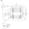
- FIG. 1 illustrates an example of a plasma display apparatus
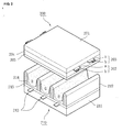
- FIG. 2 illustrates the structure of a plasma display panel of the plasma display apparatus
- FIG. 3 illustrates an example of a method for achieving gray level of an image displayed on the plasma display panel
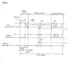
- FIG. 4 illustrates an example of a driving waveform of the plasma display apparatus
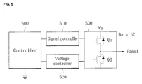
- FIG. 5 is a block diagram of a data driver of the plasma display apparatus
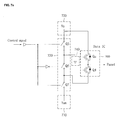
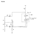
- FIGs. 6a and 6b illustrate implementations of a data driver of the plasma display apparatus according to a first embodiment
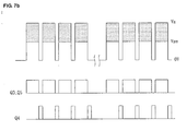
- FIG. 7a illustrates another implementation of the data driver of the plasma display apparatus according to the first embodiment
- FIG. 7b illustrates an output waveform and operation timing of the data driver of FIG. 7a
- FIG. 8 illustrates a data driver of a plasma display apparatus according to a second embodiment
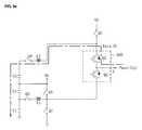
- FIGs. 9a to 9f illustrate a circuit operation of the data driver of FIG. 8 in order
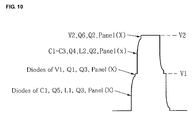
- FIG. 10 illustrates a data pulse depending on a switching operation of the data driver of FIG. 8.
- a plasma display apparatus comprises a plasma display panel 100 on which an image is displayed by processing image data input from the outside, a driver for supplying a driving pulse to electrodes of the plasma display panel 100, a controller 121 and a driving voltage generator 125.
- the driver includes a data driver 122 for supplying data to data electrodes X1 to Xm, a scan driver 123 for driving scan electrodes Y1 to Yn, and a sustain driver 124 for driving sustain electrodes Z being common electrodes.
- the controller 121 controls the data driver 122, the scan driver 123 and the sustain driver 124 when driving the plasma display panel 100.
- the driving voltage generator 125 supplies a necessary driving voltage to each of the drivers 122, 123 and 124.
- the plasma display panel 100 comprises a front substrate (not illustrated) and a rear substrate (not illustrated) which are coalesced with each other at a given distance.
- a plurality of electrodes for example, the scan electrodes Y1 to Yn and the sustain electrodes Z are formed in pairs.
- the data electrodes X1 to Xm are formed to intersect the scan electrodes Y 1 to Yn and the sustain electrodes Z.
- the data driver 122 raises the voltage of the data pulse supplied to the data electrode during the address period to a sum of a first voltage level higher than a ground level voltage and a second voltage level higher than the first voltage level.
- the scan driver 123 under the control of the controller 121, supplies a reset pulse to the scan electrodes Y1 to Yn during a reset period to initialize discharge cells corresponding to the whole screen. Further, the scan driver 123 supplies a scan reference voltage Vsc during an address period after supplying the reset pulse, and then a scan pulse falling from the scan reference voltage Vsc to a negative voltage level to the scan electrodes Y1 to Yn, thereby scanning scan electrode lines.
- the scan driver 123 supplies a sustain pulse to the scan electrodes Y1 to Yn during a sustain period to generate a sustain discharge in a discharge cell selected during the address period.
- the sustain driver 124 under the control of the controller 121, supplies a sustain pulse to the sustain electrodes Z during the sustain period.
- the scan driver 123 and the sustain driver 124 operates alternately to supply the sustain pulse.
- the controller 121 receives a vertical/horizontal synchronization signal, and generates timing control signals CTRX, CTRY and CTRZ required in each driver 122, 123 and 124.
- the controller 121 supplies the timing control signals CTRX, CTRY and CTRZ to the corresponding drivers 122, 123 and 124 to control each of the drivers 122, 123 and 124.
- the timing control signal CTRX applied to the data driver 122 includes a sampling clock for sampling data, a latch control signal, and a switch control signal for controlling on/off time of an energy recovery circuit and a driving switch element.
- the driving voltage generator 125 generates various driving voltages required in each driver 122, 123 and 124, for example, a sustain voltage Vs, a scan reference voltage Vsc, a data voltage Va, a scan voltage -Vy. These driving voltages may vary in accordance with the composition of the discharge gas or the structure of the discharge cells.
- the plasma display panel comprises a front panel 200 and a rear panel 210 which are coupled in parallel to face each other at a given distance therebetween.
- the front panel 200 comprises a front substrate 201 which is a display surface.
- the rear panel 210 comprises a rear substrate 211 constituting a rear surface.
- a plurality of scan electrodes 202 and a plurality of sustain electrodes 203 are formed in pairs on the front substrate 201, on which an image is effectively displayed, to form a plurality of maintenance electrode pairs.
- a plurality of data electrodes 213 are arranged on the rear substrate 211 to intersect with the plurality of maintenance electrode pairs.
- the scan electrode 202 and the sustain electrode 203 each comprise transparent electrodes 202a and 203a made of a transparent indium-tin-oxide (ITO) material and bus electrodes 202b and 203b made of a metal material.
- the scan electrode 202 and the sustain electrode 203 generate a mutual discharge therebetween in one discharge cell and maintain light-emissions of discharge cells.
- the scan electrode 202 and the sustain electrode 203 each may comprise either the transparent electrodes 202a and 203a or the bus electrodes 202b and 203b.
- the scan electrode 202 and the sustain electrode 203 are covered by one or more upper dielectric layers 204 to limit the discharge current and to provide insulation between the maintenance electrode pairs.
- a protective layer 205 with a deposit of MgO is formed on an upper surface of the upper dielectric layer 204 to facilitate discharge conditions.
- a plurality of well-type barrier ribs are formed on the rear substrate 211 of the rear panel 210 to form a plurality of discharge spaces, i.e., a plurality of discharge cells.
- the plurality of well-type barrier ribs comprise a transverse barrier rib (not illustrated) and a longitudinal barrier rib 212.
- the plurality of data electrodes 213 for performing an address discharge to generate vacuum ultraviolet radiation are arranged in parallel to the longitudinal barrier rib 212.
- An upper surface of the rear substrate 211 is selectively coated with Red (R), green (G) and blue (B) phosphors 214 for emitting visible light for an image display when the address discharge is performed.
- a lower dielectric layer 215 is formed between the data electrodes 213 and the phosphors 214 to protect the data electrodes 213.
- the front panel 200 and the rear panel 210 thus formed are coalesced by a sealing process such that the plasma display panel is completed.
- the drivers for driving the scan electrode 202, the sustain electrode 203 and the data electrode 213 are adhered to the plasma display panel to complete the plasma display apparatus.
- the plasma display panel is driven by dividing a frame into several subfields.
- Each of the subfields is subdivided into a reset period for initializing all the cells, an address period for selecting cells to be discharged, and a sustain period for representing gray scale in accordance with the number of discharges.
- a frame period (for example, 16.67 ms) corresponding to 1/60 sec is divided into eight subfields SF1 to SF8.
- Each of the eight subfields SF1 to SF8 is subdivided into a reset period, an address period and a sustain period.
- the duration of the reset period in a subfield is equal to the respective durations of the reset periods in the remaining subfields.
- the duration of the address period in a subfield is equal to the respective durations of the address periods in the remaining subfields.
- the duration of the sustain period of each subfield may be different from each other, and the number sustain pulses assigned during the sustain period of each subfield may be different from each other.
- FIG. 4 illustrates an example of a driving waveform of the plasma display apparatus.
- the plasma display apparatus is driven by dividing each subfield into a reset period for initializing all the cells, an address period for selecting cells to be discharged, and a sustain period for holding the selected cells in a discharge state.
- a falling pulse (Ramp-down) is simultaneously supplied to the scan electrodes Y, thereby causing a weak erase discharge within the discharge cells. Accordingly, the wall charges within the discharge cells excessively accumulated by performing the setup discharge remain uniform.
- a scan pulse (Scan) with a scan voltage -Vy is sequentially supplied to the scan electrodes Y and, at the same time, a data pulse (data) is selectively applied to the data electrodes X.
- a scan pulse (Scan) with a scan voltage -Vy is sequentially supplied to the scan electrodes Y and, at the same time, a data pulse (data) is selectively applied to the data electrodes X.
- the voltage difference between the scan pulse (Scan) and the data pulse (data) is added to the wall voltage produced during the reset period, an address discharge occurs within the discharge cells to which the data pulse (data) is supplied. Wall charges are produced inside the discharge cells selected by performing the address discharge.
- a positive voltage Vz is supplied to the sustain electrode Z during the set-down period and the address period so that an erroneous discharge does not occur between the sustain electrode Z and the scan electrode Y.
- a sustain pulse (sus) is alternately supplied to the scan electrode Y and the sustain electrode Z, thereby generating a sustain discharge.
- FIG. 5 is a block diagram of a data driver of the plasma display apparatus.
- the data driver comprises a controller 500, a driving signal output unit 530, a signal controller 510 and a voltage controller 520.
- the controller 500 supplies a control signal to the data electrode of the plasma display panel.
- the driving signal output unit 530 comprising a data electrode driving IC turns on/off switches Qu and Qd in response to the control signal supplied from controller 500 to control a pulse outputted to the data electrode of the plasma display panel.
- the signal controller 510 and the voltage controller 520 are capable of varying a reference voltage of the data electrode driving IC during a portion of the address period when a pulse for data entry is supplied.
- the signal controller 510 and the voltage controller 520 vary the reference voltage of the data electrode driving IC between a ground level voltage and a voltage higher than the ground level voltage such that when switches of the data electrode driving IC operate, the swing width of the pulse for the data entry decreases.
- the signal controller 510 and the voltage controller 520 raises the voltage of the data pulse supplied to the data electrode during the address period to a sum of a first voltage level higher than a ground level voltage and a second voltage level higher than the first voltage level. More specifically, the first voltage level higher than the ground level voltage and then the second voltage level higher than the first voltage level are supplied to the data electrode, thereby completing the supplying of the data pulse.
- the reference voltage is supplied to the data electrode driving IC is higher than the ground level voltage and is lower than a driving voltage Va of the data electrode.
- the reference voltage supplied to the data electrode by supplying a voltage Va/2 corresponding to one half the driving voltage Va or a predetermined voltage Vam, the swing width (i.e., the voltage change in the pulse for the data entry) of a switch installed inside the data electrode driving IC decreases from 0-Va to Va/2-Va. In other words, the voltage difference between both terminals of the data driver decreases such that the data driver can be driven at a low voltage, thereby stabilizing the operation of the data driver.
- the signal controller 510 supplies a pulse capable of varying the reference voltage of the driving signal output unit 530 to the driving signal output unit 530.
- the voltage controller 520 controls an output of the pulse which the signal controller 510 supplies to the signal controller 510.
- a data driver comprises a second voltage supply unit 610, a voltage supply controller 620 and an energy storing unit 640.
- the data driver further comprises a ground level voltage supply unit 630 and a driving signal output unit 600.
- the voltage supply controller 620 is formed between the second voltage supply unit 610 and the data electrode, and controls the supplying of the second voltage and the ground level voltage.
- the voltage supply controller 620 comprises a first switch Q1 and a second switch Q2 connected to each other in series.
- the ground level voltage supply unit 630 is connected to the voltage supply controller 620 and the energy storing unit 640, and supplies the ground level voltage to the data electrode.
- the second voltage supply unit 610 is commonly connected to one terminal of the first switch Q1, one terminal of the first energy storing unit C 1 and one terminal of the driving signal output unit 600.
- the ground level voltage supply unit 630 is commonly connected to the other terminal of the first switch Q1, one terminal of the second switch Q2 and the other terminal of the second energy storing unit C2.
- the other terminal of the driving signal output unit 600 is commonly connected to the other terminal of the second switch Q2, the other terminal of the first energy storing unit C 1 and one terminal of the second energy storing unit C2.
- the first voltage in the present example, one half (Va/2) the second voltage (i.e., the data voltage) is supplied to the data electrode, and the second voltage is then supplied to the data electrode.
- the second switch Q2 the ground level voltage is supplied to the data electrode.
- the second voltage is supplied to one terminal (i.e., a switch Qu) of the driving signal output unit 600, and the first voltage is supplied to the other terminal (i.e., a switch Qd) of the driving signal output unit 600. Accordingly, the difference between the voltages supplied to both switches of the driving signal output unit 600 decreases by a voltage Va/2.
- the driving signal output unit 600 can be driven at a voltage (voltage Va/2) lower than the existing voltage (i.e., voltage Va)
- power consumption in the data driver illustrated in FIG. 6a is equal to one quarter of power consumption in the existing circuit, thereby improving the driving efficiency.
- the current flowing in the driving signal output unit 600 (i.e., the data electrode driving IC) is decreased to approximately one half of the current flowing in the existing circuit such that the problem of heat generation is solved without the need for a heat sink.
- the data driver of FIG. 6a is driven at a low voltage and a low power, thereby protecting the elements of the data driver. Further, the data driver of FIG. 6a may comprise elements with a low withstanding voltage characteristic, thereby reducing the manufacturing cost.
- FIG. 6b illustrates another data driver of the plasma display apparatus.
- the data driver comprises a second voltage supply unit 611, a voltage supply controller 621 and an energy storing unit 641.
- the data driver further comprises a ground level voltage supply unit 631 and a driving signal output unit 601.
- the second voltage supply unit 611 supplies the second voltage, in the present example, the data voltage Va to the data electrode.
- the voltage supply controller 621 is formed between the second voltage supply unit 611 and the data electrode, and controls the supplying of the second voltage and the ground level voltage.
- the voltage supply controller 621 may comprise a third switch Q3 and a fourth switch Q4 connected to each other in series.
- the energy storing unit 641 divides the second voltage supplied by the second voltage supply unit 611 and stores the divided voltage.
- the energy storing unit 641 stores a voltage that is higher than the ground level voltage and is lower than the second voltage level Va, in the present example, the voltage Va/2 corresponding to one half the second voltage level Va.
- the energy storing unit 641 comprises a third energy storing unit C3 and a fourth energy storing unit C4 connected to each other in series.
- the driving signal output unit 601 outputs a voltage supplied by the second voltage supply unit 611 and a voltage supplied by the energy storing unit 641 to the data electrode through a predetermined switching operation of the driving signal output unit 601.
- the ground level voltage supply unit 631 is connected to the voltage supply controller 621 and the energy storing unit 641, and supplies the ground level voltage to the data electrode.
- the second voltage supply unit 611 is commonly connected to one terminal of the third energy storing unit C3 and one terminal of the driving signal output unit 601.
- the ground level voltage supply unit 631 is commonly connected to the other terminal of the fourth switch Q4 and the other terminal of the fourth energy storing unit C4.
- the other terminal of the driving signal output unit 601 is commonly connected to the other terminal of the third switch Q3 and one terminal of the fourth switch Q4.
- the first voltage in the present example, one half (Va/2) the second voltage (i.e., the data voltage) is supplied to the data electrode, and the second voltage is then supplied to the data electrode.
- the fourth switch Q4 the ground level voltage is supplied to the data electrode.
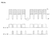
- FIG. 6c illustrates an output waveform and operation timing of the data driver of each of FIGs. 6a and 6b.
- the ground level voltage supply unit 870 comprises the seventh switch Q7 for controlling a ground level voltage source and the supplying of the ground level voltage.
- the other terminal of the seventh switch Q7 is connected to the ground level voltage source, and one terminal of the seventh switch Q7 is commonly connected to the other terminal of the first switch Q1 of the first voltage supply unit 830, the other terminal of the first inductor L1 of the first energy supply/recovery controller 820, and the other terminal of the third switch Q3 of the driving signal output 860 such that the ground level voltage supply unit 870 maintains the voltage of the data electrode at the ground level voltage.
- FIGs. 9a to 9f illustrate the circuit operation of the data driver of FIG. 8 in sequence.
- FIG. 10 illustrates a data pulse depending on a switching operation of the data driver of FIG. 8.
- the fifth switch Q5 when the fifth switch Q5 is turned off and the first switch Q1 is turned on, the first voltage V1 is supplied to the data electrode from the first voltage source and the diode of the third switch Q3 such that the data pulse is maintained at the first voltage level as illustrated in FIG. 10.
- the fourth switch Q4 is turned off and the third switch Q3 and the fifth switch Q5 are turned on such that energy remaining in the panel capacitance C p becomes stored in the first energy storing unit through the third switch Q3, the first inductor L1 and the fifth switch Q5.
- the seventh switch Q7 is turned on such that the voltage of the data electrode is maintained at the ground level voltage to complete the supplying of the data pulse.
- the low voltage driving of the plasma display apparatus can reduce the influence of the factors affecting the discharge characteristic, such as the phosphor, on the discharge characteristic such that low voltage driving prevents the factors affecting the discharge characteristic from becoming permanent. For example, even if the same number of driving pulses is supplied, the plasma display apparatus is driven at the low voltage such that the factors affecting the discharge characteristic can be prevented from becoming permanent. Accordingly, image persistence can be prevented. Further, a plasma display apparatus having the improved image quality can be provided.
Landscapes
- Engineering & Computer Science (AREA)
- Physics & Mathematics (AREA)
- Power Engineering (AREA)
- Plasma & Fusion (AREA)
- Computer Hardware Design (AREA)
- General Physics & Mathematics (AREA)
- Theoretical Computer Science (AREA)
- Control Of Indicators Other Than Cathode Ray Tubes (AREA)
- Control Of Gas Discharge Display Tubes (AREA)
Applications Claiming Priority (2)
| Application Number | Priority Date | Filing Date | Title |
|---|---|---|---|
| KR1020050083644A KR100753855B1 (ko) | 2005-09-08 | 2005-09-08 | 저전력 데이터 전극 구동회로 및 그 방법 |
| KR1020050100473A KR100747353B1 (ko) | 2005-10-24 | 2005-10-24 | 플라즈마 디스플레이 장치 및 그의 구동방법 |
Publications (2)
| Publication Number | Publication Date |
|---|---|
| EP1763002A2 true EP1763002A2 (fr) | 2007-03-14 |
| EP1763002A3 EP1763002A3 (fr) | 2007-10-31 |
Family
ID=37685929
Family Applications (1)
| Application Number | Title | Priority Date | Filing Date |
|---|---|---|---|
| EP06254703A Withdrawn EP1763002A3 (fr) | 2005-09-08 | 2006-09-08 | Dispositif d'affichage à plasma et son procédé de commande |
Country Status (3)
| Country | Link |
|---|---|
| US (1) | US20070052628A1 (fr) |
| EP (1) | EP1763002A3 (fr) |
| JP (1) | JP2007072472A (fr) |
Families Citing this family (1)
| Publication number | Priority date | Publication date | Assignee | Title |
|---|---|---|---|---|
| JP5260141B2 (ja) * | 2008-05-22 | 2013-08-14 | パナソニック株式会社 | 表示駆動装置、表示モジュールパッケージ、表示パネルモジュール及びテレビセット |
Family Cites Families (5)
| Publication number | Priority date | Publication date | Assignee | Title |
|---|---|---|---|---|
| KR100222203B1 (ko) * | 1997-03-17 | 1999-10-01 | 구자홍 | AC 플라즈마 디스플레이 패널을 위한 에너지 리커버리(recovery) 서스테인 회로 |
| JPH1185093A (ja) * | 1997-09-02 | 1999-03-30 | Pioneer Electron Corp | 表示パネル駆動装置 |
| US6667727B1 (en) * | 2000-02-08 | 2003-12-23 | Pioneer Corporation | Plasma display apparatus |
| WO2003041041A2 (fr) * | 2001-11-06 | 2003-05-15 | Pioneer Corporation | Appareil d'entrainement de panneau d'affichage possedant une structure capable de reduire une perte de puissance |
| KR100484175B1 (ko) * | 2002-11-08 | 2005-04-18 | 삼성전자주식회사 | 고효율 플라즈마 디스플레이 패널 구동 장치 및 방법 |
-
2006
- 2006-09-07 US US11/516,563 patent/US20070052628A1/en not_active Abandoned
- 2006-09-08 JP JP2006244723A patent/JP2007072472A/ja not_active Withdrawn
- 2006-09-08 EP EP06254703A patent/EP1763002A3/fr not_active Withdrawn
Also Published As
| Publication number | Publication date |
|---|---|
| US20070052628A1 (en) | 2007-03-08 |
| EP1763002A3 (fr) | 2007-10-31 |
| JP2007072472A (ja) | 2007-03-22 |
Similar Documents
| Publication | Publication Date | Title |
|---|---|---|
| EP2091037A2 (fr) | Appareil d'affichage à plasma | |
| US20090109138A1 (en) | Plsma display apparatus | |
| CN100446060C (zh) | 等离子体显示设备及其驱动方法 | |
| US7852292B2 (en) | Plasma display apparatus and driving method thereof | |
| KR100605763B1 (ko) | 플라즈마 디스플레이 패널 구동 장치 및 방법 | |
| EP1763002A2 (fr) | Appareil d'affichage à plasma et procédé de commande correspondant | |
| US20060033683A1 (en) | Plasma display apparatus and driving method thereof | |
| CN100433092C (zh) | 等离子显示设备及其驱动方法 | |
| EP1748408A2 (fr) | Procédé de commande d'un appareil d'affichage à plasma | |
| KR20060090052A (ko) | 플라즈마 디스플레이 장치 및 플라즈마 디스플레이 패널의구동장치 | |
| EP1677280A2 (fr) | Appareil d'affichage à plasma et son procédé de commande | |
| US7889155B2 (en) | Plasma display apparatus | |
| KR100844821B1 (ko) | 플라즈마 디스플레이 장치 및 그의 구동방법 | |
| EP1780694A2 (fr) | Appareil d'affichage à plasma | |
| KR100747353B1 (ko) | 플라즈마 디스플레이 장치 및 그의 구동방법 | |
| KR100681034B1 (ko) | 플라즈마 디스플레이 장치 및 그의 구동방법 | |
| US20070085772A1 (en) | Plasma display apparatus and method of driving the same | |
| US20080055204A1 (en) | Plasma display apparatus and method of driving the same | |
| KR100681018B1 (ko) | 플라즈마 표시장치 및 그 구동방법 | |
| KR100646218B1 (ko) | 플라즈마 디스플레이 패널의 구동장치 | |
| KR100829251B1 (ko) | 플라즈마 디스플레이 장치 및 그의 구동방법 | |
| US20070115220A1 (en) | Plasma display apparatus | |
| US20070152588A1 (en) | Plasma display panel | |
| KR20060091200A (ko) | 플라즈마 디스플레이 패널 구동장치 | |
| KR20070004392A (ko) | 플라즈마 디스플레이 장치 및 그 구동 방법 |
Legal Events
| Date | Code | Title | Description |
|---|---|---|---|
| PUAI | Public reference made under article 153(3) epc to a published international application that has entered the european phase |
Free format text: ORIGINAL CODE: 0009012 |
|
| AK | Designated contracting states |
Kind code of ref document: A2 Designated state(s): AT BE BG CH CY CZ DE DK EE ES FI FR GB GR HU IE IS IT LI LT LU LV MC NL PL PT RO SE SI SK TR |
|
| AX | Request for extension of the european patent |
Extension state: AL BA HR MK YU |
|
| RIC1 | Information provided on ipc code assigned before grant |
Ipc: G09G 3/288 20060101AFI20070213BHEP |
|
| PUAL | Search report despatched |
Free format text: ORIGINAL CODE: 0009013 |
|
| AK | Designated contracting states |
Kind code of ref document: A3 Designated state(s): AT BE BG CH CY CZ DE DK EE ES FI FR GB GR HU IE IS IT LI LT LU LV MC NL PL PT RO SE SI SK TR |
|
| AX | Request for extension of the european patent |
Extension state: AL BA HR MK YU |
|
| AKX | Designation fees paid | ||
| REG | Reference to a national code |
Ref country code: DE Ref legal event code: 8566 |
|
| STAA | Information on the status of an ep patent application or granted ep patent |
Free format text: STATUS: THE APPLICATION IS DEEMED TO BE WITHDRAWN |
|
| 18D | Application deemed to be withdrawn |
Effective date: 20080503 |