EP1763043B1 - Structure inductive - Google Patents
Structure inductive Download PDFInfo
- Publication number
- EP1763043B1 EP1763043B1 EP05425635A EP05425635A EP1763043B1 EP 1763043 B1 EP1763043 B1 EP 1763043B1 EP 05425635 A EP05425635 A EP 05425635A EP 05425635 A EP05425635 A EP 05425635A EP 1763043 B1 EP1763043 B1 EP 1763043B1
- Authority
- EP
- European Patent Office
- Prior art keywords
- inductive structure
- structure according
- package substrate
- inductive
- ferromagnetic
- Prior art date
- Legal status (The legal status is an assumption and is not a legal conclusion. Google has not performed a legal analysis and makes no representation as to the accuracy of the status listed.)
- Expired - Lifetime
Links
Images


Classifications
-
- H—ELECTRICITY
- H10—SEMICONDUCTOR DEVICES; ELECTRIC SOLID-STATE DEVICES NOT OTHERWISE PROVIDED FOR
- H10W—GENERIC PACKAGES, INTERCONNECTIONS, CONNECTORS OR OTHER CONSTRUCTIONAL DETAILS OF DEVICES COVERED BY CLASS H10
- H10W90/00—Package configurations
-
- H—ELECTRICITY
- H01—ELECTRIC ELEMENTS
- H01F—MAGNETS; INDUCTANCES; TRANSFORMERS; SELECTION OF MATERIALS FOR THEIR MAGNETIC PROPERTIES
- H01F17/00—Fixed inductances of the signal type
- H01F17/0006—Printed inductances
- H01F17/0033—Printed inductances with the coil helically wound around a magnetic core
-
- H—ELECTRICITY
- H01—ELECTRIC ELEMENTS
- H01F—MAGNETS; INDUCTANCES; TRANSFORMERS; SELECTION OF MATERIALS FOR THEIR MAGNETIC PROPERTIES
- H01F41/00—Apparatus or processes specially adapted for manufacturing or assembling magnets, inductances or transformers; Apparatus or processes specially adapted for manufacturing materials characterised by their magnetic properties
- H01F41/02—Apparatus or processes specially adapted for manufacturing or assembling magnets, inductances or transformers; Apparatus or processes specially adapted for manufacturing materials characterised by their magnetic properties for manufacturing cores, coils, or magnets
- H01F41/04—Apparatus or processes specially adapted for manufacturing or assembling magnets, inductances or transformers; Apparatus or processes specially adapted for manufacturing materials characterised by their magnetic properties for manufacturing cores, coils, or magnets for manufacturing coils
- H01F41/041—Printed circuit coils
- H01F41/046—Printed circuit coils structurally combined with ferromagnetic material
-
- H—ELECTRICITY
- H10—SEMICONDUCTOR DEVICES; ELECTRIC SOLID-STATE DEVICES NOT OTHERWISE PROVIDED FOR
- H10W—GENERIC PACKAGES, INTERCONNECTIONS, CONNECTORS OR OTHER CONSTRUCTIONAL DETAILS OF DEVICES COVERED BY CLASS H10
- H10W44/00—Electrical arrangements for controlling or matching impedance
- H10W44/501—Inductive arrangements
-
- H—ELECTRICITY
- H01—ELECTRIC ELEMENTS
- H01F—MAGNETS; INDUCTANCES; TRANSFORMERS; SELECTION OF MATERIALS FOR THEIR MAGNETIC PROPERTIES
- H01F17/00—Fixed inductances of the signal type
- H01F17/0006—Printed inductances
- H01F17/0013—Printed inductances with stacked layers
-
- H—ELECTRICITY
- H10—SEMICONDUCTOR DEVICES; ELECTRIC SOLID-STATE DEVICES NOT OTHERWISE PROVIDED FOR
- H10W—GENERIC PACKAGES, INTERCONNECTIONS, CONNECTORS OR OTHER CONSTRUCTIONAL DETAILS OF DEVICES COVERED BY CLASS H10
- H10W72/00—Interconnections or connectors in packages
- H10W72/50—Bond wires
- H10W72/531—Shapes of wire connectors
- H10W72/536—Shapes of wire connectors the connected ends being ball-shaped
-
- H—ELECTRICITY
- H10—SEMICONDUCTOR DEVICES; ELECTRIC SOLID-STATE DEVICES NOT OTHERWISE PROVIDED FOR
- H10W—GENERIC PACKAGES, INTERCONNECTIONS, CONNECTORS OR OTHER CONSTRUCTIONAL DETAILS OF DEVICES COVERED BY CLASS H10
- H10W72/00—Interconnections or connectors in packages
- H10W72/50—Bond wires
- H10W72/541—Dispositions of bond wires
- H10W72/547—Dispositions of multiple bond wires
- H10W72/5473—Dispositions of multiple bond wires multiple bond wires connected to a common bond pad
-
- H—ELECTRICITY
- H10—SEMICONDUCTOR DEVICES; ELECTRIC SOLID-STATE DEVICES NOT OTHERWISE PROVIDED FOR
- H10W—GENERIC PACKAGES, INTERCONNECTIONS, CONNECTORS OR OTHER CONSTRUCTIONAL DETAILS OF DEVICES COVERED BY CLASS H10
- H10W74/00—Encapsulations, e.g. protective coatings
-
- Y—GENERAL TAGGING OF NEW TECHNOLOGICAL DEVELOPMENTS; GENERAL TAGGING OF CROSS-SECTIONAL TECHNOLOGIES SPANNING OVER SEVERAL SECTIONS OF THE IPC; TECHNICAL SUBJECTS COVERED BY FORMER USPC CROSS-REFERENCE ART COLLECTIONS [XRACs] AND DIGESTS
- Y10—TECHNICAL SUBJECTS COVERED BY FORMER USPC
- Y10T—TECHNICAL SUBJECTS COVERED BY FORMER US CLASSIFICATION
- Y10T29/00—Metal working
- Y10T29/49—Method of mechanical manufacture
- Y10T29/49002—Electrical device making
- Y10T29/4902—Electromagnet, transformer or inductor
Definitions
- the present invention relates to an inductive structure.
- the invention relates to an inductive structure of the type comprising at least a winding comprising at least a coil and developed around a ferromagnetic core.
- the invention also relates to a method for integrating an inductive structure in an electronic device package.
- the invention particularly, but not exclusively, relates to a multichip device and the following description is made with reference to this field of application by way of illustration only.
- Three-dimension circuit solutions have also been proposed, in particular exploiting the z dimension of electronic devices integrated in chip or die, i.e. a dimension orthogonal to a development plane of the chip, by packing, one above the other, more dice and leading to the emergence of the so called stacked devices or multichip.
- the discrete inductors currently on sale with significant saturation currents (higher than 0,5A) and with inductance value around ⁇ H have such dimensions that they cannot be integrated in a SIP.
- the discrete components, so as to be integrated in a package must have greatest dimensions equal to a SMD0402 (0,5 mm x 1 mm and 0,5 mm of thickness) thus with thickness lower than 700 ⁇ m.
- the discrete inductors with inductance values in the order of the ten of ⁇ H and with saturation currents higher than 0,5A have instead thickness higher than 1mm.
- Such document describes an inductor realised with the bonding wires thanks to the presence of pairs of bonding terminals or pads realised on a substrate of a semiconductor device and of one or more bonding wires configured so as to realise a ring and thus an inductive winding.
- An injection step is also provided of an epoxy resin to complete the package containing the inductor thus realised.
- planar inductors comprising the steps of electroplating to add thicker layer of less conductive ferromagnetic material to a core which is formed at least in part by electroless plating.
- the ferroelectric layers are formed by dipping the dielectric surface in a solution containing catalytic metal particles. It is to be noted that such proposed method is deeply tied to the features of the layer whereon the ferroelectric layers are formed.
- the technical problem underlying the present invention is that of devising an integrated inductive structure having such structural and functional characteristics as to realise geometric structures of electronic components integrated in a multichip and which use the magnetic properties of one or more coils, simultaneously overcoming the limits and the drawbacks still affecting the devices realised according to the prior art.
- the solution idea underlying the present invention is that of realising a winding around a ferromagnetic core realised by means of a multilayer structure of a ferromagnetic material deposited on a package substrate of a multichip device, such as for example a SIP or a stacked device.
- the winding comprises at least a coil realised by exploiting the bonding wires and/or the tracks of a first metallisation layer of the package substrate of the multichip device.
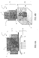
- the inductive structure 1 comprises a winding 2 developed around a ferromagnetic core 3.
- the ferromagnetic core 3 is realised by a ferromagnetic structure suitably arranged above a package substrate so as to be contained inside the winding 2, as it will be clarified hereafter in the description, this package comprising besides the inductive structure 1 at least a further electronic device.
- the ferromagnetic structure is realised by means of a multilayer 3 obtained by overlapping different layers 3a of flat ferromagnetic material overlapped and glued onto each other, as shown in Figure 1B , and it thus allows to obtain a ferromagnetic core of desired dimensions for the inductive structure 1.
- the multilayer ferromagnetic structure 3 comprises an overlapping of layers 3a of flat ferromagnetic material and of layers 3b of insulating material, suitably adhesive, alternated with each other, its realisation resulting to be easily inserted in an integration process of a multichip device, as it will be clarified hereafter in the description.
- the multilayer ferromagnetic structure 3 inserted inside the winding 2 allows to confine the magnetic field of the inductive structure 1 and not to notably influence the interconnections close thereto inside a package.
- the multilayer ferromagnetic structure 3 has a closed configuration, substantially ring-shaped, as shown in Figure 1A .
- the multilayer ferromagnetic structure 3 is substantially a rectangular plate equipped with a central opening, also preferably rectangular.
- the multilayer ferromagnetic structure 3 advantageously allows to obtain significant inductance values for the integrated inductor realised by the inductive structure 1 and thus it allows its use inside a package for integrated circuits, the multilayer ferromagnetic structure 3 being deposited on a package substrate 4, as shown in greater detail in Figure 2 .
- the multilayer ferromagnetic structure 3 has been realised in the ferromagnetic material commercially available with the name VITROVAC 6150.
- This material has relative magnetic mobilities equal to 1300 and, in the configuration shown in Figure 1A , allows to implement an integrated inductor of 15 ⁇ H with saturation currents close to the Ampere.
- the thickness of the ferromagnetic layers or bands 3a of VITROVAC 6150 on sale is equal to 25 ⁇ m, to obtain the multilayer ferromagnetic structure 3 of suitable thickness, different layers of this material have been overlapped, suitably glued to each other.
- the pattern of the magnetic field inside the multilayer ferromagnetic structure 2 so obtained is schematically shown in Figure 3 and it results to be in the order 1T with highest current equal to 0,6A and parasite resistance equal to 3,5 Ohm.
- the inductive structure 1 comprises a winding 2 equipped with a plurality of coils 5, each one comprising a first portion 5a, comprising for example a length portion D of a metallisation line 5c realised on the package substrate 4, as well as a second portion 5b, made for example of a bonding wire 5d, joined to each other in a ring-like configuration to form the coil 5, as shown in Figure 3 .
- the bonding wire 5d connects a first X1 and a second end X2 of the portion 5a of the metallisation line 5c so as to form the coil 5.
- the multilayer ferromagnetic structure 3 is arranged above the package substrate 4 so as to be contained inside the coil 5.
- the multilayer ferromagnetic structure 3 is arranged above the metallisation line 5c, within the first and the second ends X1 and X2 of the same, the bonding wire 5d suitably passing above this structure 3 to connect the first and the second ends X1 and X2.
- the winding is not a closed path, in other words if the ends X1 and X2 are interconnected by using the first metal level of the substrate, they are not interconnected through a bonding wire so as to allow that the current flows in the winding in a desired way.
- the multilayer ferromagnetic structure 3 is suitably coated, at least in correspondence with a lower face thereof, arranged next to the package substrate 4 and to an upper face thereof, arranged next to an apical point Y of the bonding wire 5d, by means of an electrically insulating glue layer so as not to create conductive short-circuits between the coils.
- this electrically insulating glue layer is arranged on all the faces of the multilayer ferromagnetic structure 3.
- the entire multilayer ferromagnetic structure 3 is coated with an electrically insulating glue.
- the rules for the positioning of the bondfingers (not shown since conventional) and of the bonding wires used for the realisation of a generic multichip device are suitably respected, so as not to have any problems of short-circuits between the bonding wires in consequence of the resin injection and of the moulding carried out on the multichip device itself.
- the integrated inductor realised by means of the inductive structure described finds advantageous application, for example, in step-up voltage converters where it is used to carry out switches of an operative voltage.
- the sole limitations of the integrated inductor thus obtained for these applications are constituted by the characteristics of the ferromagnetic material used and they are linked to the highest switch frequency of the magnetisation of the material itself and to the saturation magnetic field.
- the inductive structure 1 is also suitable to implement a transformer, as schematically shown in Figure 3 .
- the transformer comprises, in particular, a multilayer ferromagnetic structure 3, which can be suitably realised on a package substrate of a multichip device in case the transformer is integrated in such multichip device, whereon a first or primary winding 2 and a second or secondary winding 6 are arranged, both realised as previously described and comprising pluralities of coils also realised as already described.
- the number of coils comprised in the primary 2 and secondary windings 6 allow to dimension the transformer obtained by means of the inductive structure 1 as desired.
- the multilayer ferromagnetic structure 3 has a closed configuration, substantially ring-like shaped, in particular with rectangular plan and equipped with a central opening, also preferably rectangular.
- a transformer suitable to be comprised in a package of multichip device in particular a stacked device or a SIP.
- the transformer realised by the integrated inductive structure 1 according to the invention can be used for frequencies higher than the tens of kHz.
- the integrated inductive structure 1 is also suitable to implement a sensor schematically shown in Figure 5 .
- the multilayer ferromagnetic structure 3 has a substantially bar-like shape, in particular squared, with the coils of the winding 2 wound thereon.
- the sensor configuration shown in Figure 5 is able to realise a proximity sensor based on the magnetic field, a passage sensor or also a position sensor to be applied to a stator or to a rotor of a robot motor.
- the variation of the magnetic flux linked with its winding 2 can be determined.
- the integrated inductive structure 1 can be used for realising a relay, schematically shown in Figures 6A and 6B .
- the integrated inductive structure 1 implementing the relay comprises, in this case, a first portion 1a configured as the sensor of Figure 5 and comprising in turn a multilayer ferromagnetic structure 2 whereon a winding 2 is wound as well as a second portion 1b, in particular a triggering portion, substantially suitable to realise a switch.
- the triggering portion 1b essentially comprises a first bonding wire 7a, in particular realised with material sensitive to the magnetic field, such as for example iron or nickel, as well as a further non-ferromagnetic wire 7b (shown in Figure 6A by a second bonding wire 7b).
- the triggering portion 1b comprises a first wire 8 and a second switch 9.
- the first wire 8 is a mobile element able to create the electric contact with the second wire 9.
- the first wire 8 is realised by means of a strip 8a of ferromagnetic material equipped with a metallic tongue 8b and the second wire 9 is a switch.
- a magnetic field B is applied, inside the triggering portion 1b a force is generated able to move the metallic tongue 8b in the direction of the second wire 9: it is thus possible to short-circuit the two wires 8 and 9 and to have through them a current flow.
- Both the wires 8 and 9 are glued with a conductive glue (or welded) on a pad of the package substrate of a multichip device with which the integrated inductive structure 1 suitable to implement the relay is integrated and in this way they are short-circuited with the relative connection.
- a conductive glue or welded
- the triggering portion 1b comprises a ferromagnetic contact which should be free to move. Therefore, the area wherein this inductive structure 1 is realised does not have to be covered by resin.
- the inductive structure 1 thus comprises a protective plastic casing for the area of the mobile contact. In a preferred embodiment of the inductive structure 1 according to the invention, inside this protective area the void is created so as to avoid problems of oxidation of the metallic and ferromagnetic contacts.
- the winding 2 is realised without exploiting the bonding wires, but through suitable routing of a first and of a second plurality of tracks in different layers of the package substrate of the multichip device wherein the winding 2 is integrated.
- a first portion 2a of the winding 2 comprising this first plurality of tracks and realised in a first layer 4a of the package substrate 4 and a second portion 2b comprising this second plurality of tracks and realised in a second layer 4b of the package substrate 4, suitable vias being provided for the contact of said pluralities of tracks.
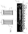
- Figure 8 schematically shows a section of a multichip device, in particular a SIP 10 comprising at least an integrated inductive structure 1 realised according to the invention, suitable to implement an inductor, a sensor or a relay.
- the SIP 10 comprises the integrated inductive structure 1 realised next to a stack 11 of a first 11a and of a second chip 11b, mounted on a package substrate 4, in particular equipped with a ball grid array 12, and possibly separated by an interposer 13.
- the present invention also relates to a method for integrating an inductive structure 1 on a package substrate 4, in particular in a multichip device such as a stacked device or a SIP.
- the method according to the invention comprises the steps of:
- the method also provides the steps of:
- this step of realising an integrated inductive structure 1 comprises the steps of:
- the electric connection of a first X1 and of a second end X2 of the portion 5a of the metallisation line 5c is carried out by means of bonding above the multilayer ferromagnetic structure 3, as shown in Figures 1A and 2 .
- a bonding wire 5d is connected to the first X1 and to the second end X2 of the portion 5a of the metallisation line 5c in a ring-like configuration to form the coil 5, as shown in Figure 3 .
- the coil 5 comprises a first portion corresponding to the portion 5a of the metallisation line 5c and a second portion comprising the bonding wire 5d joined to each other to form a ring and thus a coil 5 of the winding 2.
- a winding 2 comprising a plurality of coils 5 by means of a plurality of metallisation lines and bonding wires.
- the method according to the invention advantageously provides that this bonding step is realised simultaneously with at least one bonding step of the process flow suitable to realise the chip stack 11.
- this electric connection of a first X1 and of a second end X2 of the portion 5a of the metallisation line 5c is realised through routing of at least one further portion of a further or second metallisation line realised in a second layer 4b of the package substrate 4 distinct from a first layer 4a of this package substrate 4 wherein the first metallisation line 5c is realised.
- the method also provides that the step of depositing the multilayer ferromagnetic structure 3 of the package substrate 4 comprises the steps of:
- the method also provides that the step of depositing the multilayer ferromagnetic structure 3 on the package substrate 4 comprises the steps of:
- this step of depositing the multilayer ferromagnetic structure 3 on the package substrate 4 is realised simultaneously with at least one step of depositing at least one chip of the stack.
- a small block of ferromagnetic material being cut and already packed, to form a multilayer material can be treated in an identical way as the "dices", i.e. it can be placed on the substrate with the suitable pick and place machines.
- the method according to the invention comprises, before the step of realising the winding 2, at least one coating step of the multilayer ferromagnetic structure 3 by means of an insulating layer, in particular an insulating glue layer.
- this coating step provides a deposition of this insulating layer on a lower face of the multilayer ferromagnetic structure 2, arranged next to the package substrate 4 and on an upper face thereof, opposite the lower face.
- this insulating layer is deposited on all the faces of the multilayer ferromagnetic structure 2.
- the inductive structure 1 proposed allows to realise an inductor, a transformer, a sensor and a relay inside a package of electronic device.
- the proposed inductive structure 1 by using the proposed inductive structure 1, it is possible to increase the potentiality of the systems that can be realised in a package, for example by allowing the insertion inside the package of inductors with considerable inductance values suitable for particular applications and with saturation currents close to the Ampere, without risking to interfere in a significant way with the rest of the system integrated therewith.
Landscapes
- Engineering & Computer Science (AREA)
- Power Engineering (AREA)
- Microelectronics & Electronic Packaging (AREA)
- Manufacturing & Machinery (AREA)
- Coils Or Transformers For Communication (AREA)
Claims (33)
- Structure inductive du type comprenant au moins un enroulement (2) comprenant au moins une bobine (5) et développée autour d'un noyau ferromagnétique (3), ladite structure inductive (1) étant intégrée à un emballage d'un dispositif électronique (11), caractérisée en ce que ledit noyau ferromagnétique (3) est une multicouche réalisée au moyen d'une structure ferromagnétique agencée au-dessus d'un substrat (4) dudit emballage et comprend une superposition d'une pluralité de couches (3a) de matériau ferromagnétique plat superposées l'une sur l'autre et d'une pluralité de couches (3b) de matériau isolant en alternance avec ladite pluralité de couches (3a) de matériau ferromagnétique plat.
- Structure inductive selon la revendication 1, caractérisée en ce que lesdites couches (3b) de matériau isolant sont réalisées dans un matériau adhésif.
- Structure inductive selon la revendication 1, caractérisée en ce que ladite structure ferromagnétique multicouche (3) a une configuration fermée, sensiblement en forme d'anneau.
- Structure inductive selon la revendication 1, caractérisée en ce que ladite au moins une bobine (5) comprend une première partie (5a) comprenant une partie d'une ligne de métallisation (5c) réalisée dans ledit substrat d'emballage (4), ainsi qu'une deuxième partie (5b), ladite deuxième partie (5b) connectant des première et deuxième extrémités (X1, X2) de ladite première partie (5a) pour former des bobines d'un enroulement continu.
- Structure inductive selon la revendication 4, caractérisée en ce que ladite deuxième partie (5b) comprend un fil de liaison (5d).
- Structure inductive selon la revendication 4, caractérisée en ce que ladite deuxième partie (5b) comprend une partie d'une autre ligne de métallisation réalisée dans une couche (4b) dudit substrat d'emballage (4) distincte d'une couche (4a) dudit substrat d'emballage (4) dans laquelle ladite ligne de métallisation (5c) est réalisée.
- Structure inductive selon la revendication 6, caractérisée en ce qu'elle comprend des vias de contact appropriés de ladite ligne de métallisation (5c) et de ladite autre ligne de métallisation.
- Structure inductive selon la revendication 1, caractérisée en ce qu'elle comprend une couche de revêtement isolant pour ladite structure ferromagnétique multicouche (3).
- Structure inductive selon la revendication 8, caractérisée en ce que ladite couche de revêtement isolant couvre ladite structure ferromagnétique multicouche (3) en correspondance avec une face inférieure de celle-ci, agencée à côté dudit substrat d'emballage (4) et d'une face supérieure de celle-ci à l'opposé de ladite face inférieure.
- Structure inductive selon la revendication 8, caractérisée en ce que ladite couche de revêtement isolant couvre ladite structure ferromagnétique multicouche (3) en correspondance avec toutes les faces de celle-ci.
- Structure inductive selon la revendication 8, caractérisée en ce que ladite couche de revêtement isolant comprend une couche de colle électriquement isolante.
- Structure inductive selon la revendication 1, caractérisée en ce qu'elle réalise un transformateur et en ce qu'elle comprend un autre enroulement (6) agencé au-dessus de ladite structure ferromagnétique multicouche (3).
- Structure inductive selon la revendication 12, caractérisée en ce que ladite structure ferromagnétique multicouche (3) a une configuration fermée sensiblement en forme d'anneau.
- Structure inductive selon la revendication 1, caractérisée en ce qu'elle réalise un capteur et en ce que ladite structure ferromagnétique multicouche (3) est sensiblement en forme de barre.
- Structure inductive selon la revendication 1, caractérisée en ce qu'elle réalise un relais et en ce qu'elle comprend une première partie (1a) comprenant ladite structure ferromagnétique multicouche (3) sur laquelle ledit enroulement (2) est enroulé et une deuxième partie de déclenchement (1b) appropriée pour réaliser un commutateur.
- Structure inductive selon la revendication 15, caractérisée en ce que ladite deuxième partie de déclenchement (1b) comprend au moins un premier fil (7a, 8) réalisé avec un matériau sensible au champ magnétique et avec un deuxième fil (7b, 9) agencé à côté de ce premier fil (7a), placé aussi à l'intérieur d'un champ magnétique (B) généré par ladite première partie (1a) et capable de se déplacer pour entrer en contact avec ledit deuxième fil (7b).
- Structure inductive selon la revendication 16, caractérisée en ce que ledit deuxième fil (7b) est réalisé dans un matériau non ferromagnétique.
- Structure inductive selon la revendication 16, caractérisée en ce que ledit premier fil (7a) comprend un fil de liaison.
- Structure inductive selon la revendication 16, caractérisée en ce que ledit deuxième fil (7b) comprend un fil de liaison.
- Structure inductive selon la revendication 16, caractérisée en ce que ledit premier fil (8) comprend une bande (8a) de matériau ferromagnétique munie d'une langue métallique (8b) capable de se déplacer dans une direction vers ledit deuxième conducteur (9), respectivement en direction opposée à ce deuxième conducteur (9).
- Structure inductive selon la revendication 20, caractérisée en ce que lesdits premier et deuxième fils (8, 9) sont collés avec une colle conductrice ou soudés sur un patin dudit substrat d'emballage (4).
- Structure inductive selon la revendication 15, caractérisée en ce que ladite deuxième partie de déclenchement (1b) comprend une enveloppe plastique protectrice.
- Structure inductive selon la revendication 22, caractérisée en ce qu'un vide est créé dans ladite enveloppe plastique protectrice.
- Structure inductive selon la revendication 1, caractérisée en ce que ledit dispositif électronique (11) est un dispositif à puces multiples.
- Procédé pour intégrer une structure inductive (1) sur un substrat d'emballage (4) du type comprenant les étapes consistant à :- fournir un substrat d'emballage (4) ;- réaliser, dans ledit substrat d'emballage (4), au moins une ligne de métallisation (5c) ;- intégrer, sur ledit substrat d'emballage (4), au moins un dispositif électronique (11) ;- réaliser, sur ledit substrat d'emballage (4), une structure inductive (1) à côté dudit dispositif électronique (11), caractérisé en ce que ladite étape de réalisation comprend en outre les étapes consistant à :- déposer une structure ferromagnétique multicouche (3) sur ledit substrat d'emballage (4) à côté dudit dispositif électronique ; et- réaliser au moins une bobine (5) d'un enroulement (2) de ladite structure inductive intégrée (1) au moyen d'une connexion électrique d'une partie (5a) de ladite ligne de métallisation (5c) ;
et en ce que ladite étape de dépôt de ladite structure ferromagnétique multicouche (3) sur ledit substrat d'emballage (4) comprend les étapes consistant à :- déposer une pluralité de couches (3a) de matériau ferromagnétique plat superposées l'une sur l'autre ; et- déposer une pluralité de couches (3a) de matériau ferromagnétique plat et une pluralité de couches (3b) de matériau adhésif, superposées l'une sur l'autre en alternance. - Procédé selon la revendication 25, caractérisé en ce que ladite étape de connexion électrique d'une partie (5a) de ladite ligne de métallisation (5c) comprend une étape de liaison pour connecter électriquement des première et deuxième extrémités (X1, X2) de l'une desdites parties (5a) de ladite ligne de métallisation (5c), ladite étape de liaison étant effectuée au-dessus de ladite structure ferromagnétique multicouche (3).
- Procédé selon la revendication 26, caractérisé en ce que ladite étape de liaison peut être réalisée simultanément avec au moins une étape de liaison de flux de processus approprié pour réaliser ledit dispositif électronique (11).
- Procédé selon la revendication 25, caractérisé en ce que ladite étape de connexion électrique d'une partie (5a) de ladite ligne de métallisation (5c) comprend une étape d'acheminement d'au moins une autre partie d'une autre ligne de métallisation réalisée dans une couche (4b) dudit substrat d'emballage (4) distincte de ladite couche (4a) dudit substrat d'emballage (4) dans laquelle ladite ligne de métallisation (5c) est réalisée.
- Procédé selon la revendication 25, caractérisé en ce que ladite étape de dépôt de ladite structure ferromagnétique multicouche (3) sur ledit substrat d'emballage (4) peut être réalisée simultanément avec au moins une étape de réalisation dudit dispositif électronique (11).
- Procédé selon la revendication 25, caractérisé en ce qu'il comprend en outre une étape de revêtement de ladite structure ferromagnétique multicouche (3) au moyen d'une couche isolante.
- Procédé selon la revendication 30, caractérisé en ce que ladite étape de revêtement implique une face inférieure de ladite structure ferromagnétique multicouche (3) agencée à côté dudit substrat d'emballage (4) et une face supérieure de celle-ci à l'opposé de ladite face inférieure.
- Procédé selon la revendication 30, caractérisé en ce que ladite étape de revêtement implique toutes les faces de ladite structure ferromagnétique multicouche (3).
- Procédé selon la revendication 30, caractérisé en ce que ledit dispositif électronique (11) est un dispositif à puces multiples.
Priority Applications (3)
| Application Number | Priority Date | Filing Date | Title |
|---|---|---|---|
| DE602005020005T DE602005020005D1 (de) | 2005-09-09 | 2005-09-09 | Induktive Anordnung |
| EP05425635A EP1763043B1 (fr) | 2005-09-09 | 2005-09-09 | Structure inductive |
| US11/530,320 US20070062027A1 (en) | 2005-09-09 | 2006-09-08 | Inductive structure |
Applications Claiming Priority (1)
| Application Number | Priority Date | Filing Date | Title |
|---|---|---|---|
| EP05425635A EP1763043B1 (fr) | 2005-09-09 | 2005-09-09 | Structure inductive |
Publications (2)
| Publication Number | Publication Date |
|---|---|
| EP1763043A1 EP1763043A1 (fr) | 2007-03-14 |
| EP1763043B1 true EP1763043B1 (fr) | 2010-03-17 |
Family
ID=35717593
Family Applications (1)
| Application Number | Title | Priority Date | Filing Date |
|---|---|---|---|
| EP05425635A Expired - Lifetime EP1763043B1 (fr) | 2005-09-09 | 2005-09-09 | Structure inductive |
Country Status (3)
| Country | Link |
|---|---|
| US (1) | US20070062027A1 (fr) |
| EP (1) | EP1763043B1 (fr) |
| DE (1) | DE602005020005D1 (fr) |
Families Citing this family (27)
| Publication number | Priority date | Publication date | Assignee | Title |
|---|---|---|---|---|
| US9601412B2 (en) * | 2007-06-08 | 2017-03-21 | Cyntec Co., Ltd. | Three-dimensional package structure |
| US8134425B2 (en) * | 2007-12-13 | 2012-03-13 | Broadcom Corporation | Method and system for filters embedded in an integrated circuit package |
| US8384500B2 (en) | 2007-12-13 | 2013-02-26 | Broadcom Corporation | Method and system for MEMS switches fabricated in an integrated circuit package |
| US7859360B2 (en) * | 2007-12-13 | 2010-12-28 | Broadcom Corporation | Method and system for controlling MEMS switches in an integrated circuit package |
| US8115567B2 (en) * | 2007-12-13 | 2012-02-14 | Broadcom Corporation | Method and system for matching networks embedded in an integrated circuit package |
| US20090153281A1 (en) * | 2007-12-13 | 2009-06-18 | Ahmadreza Rofougaran | Method and system for an integrated circuit package with ferri/ferromagnetic layers |
| US7863998B2 (en) * | 2008-02-25 | 2011-01-04 | Broadcom Corporation | Method and system for processing signals via directional couplers embedded in an integrated circuit package |
| US7859359B2 (en) * | 2008-02-25 | 2010-12-28 | Broadcom Corporation | Method and system for a balun embedded in an integrated circuit package |
| US20090219908A1 (en) * | 2008-02-29 | 2009-09-03 | Ahmadreza Rofougaran | Method and system for processing signals via diplexers embedded in an integrated circuit package |
| WO2009118694A1 (fr) * | 2008-03-25 | 2009-10-01 | Nxp B.V. | Élément inductif à haute densité et haute qualité 3d intégré |
| US7982555B2 (en) | 2008-03-28 | 2011-07-19 | Broadcom Corporation | Method and system for processing signals via power splitters embedded in an integrated circuit package |
| US8269344B2 (en) * | 2008-03-28 | 2012-09-18 | Broadcom Corporation | Method and system for inter-chip communication via integrated circuit package waveguides |
| US20090309683A1 (en) * | 2008-06-16 | 2009-12-17 | Cochran William T | Sensor inductors, sensors for monitoring movements and positioning, apparatus, systems and methods therefore |
| US8384596B2 (en) * | 2008-06-19 | 2013-02-26 | Broadcom Corporation | Method and system for inter-chip communication via integrated circuit package antennas |
| US8450846B2 (en) * | 2008-06-19 | 2013-05-28 | Broadcom Corporation | Method and system for communicating via flip-chip die and package waveguides |
| US8238842B2 (en) * | 2009-03-03 | 2012-08-07 | Broadcom Corporation | Method and system for an on-chip and/or an on-package transmit/receive switch and antenna |
| US8447250B2 (en) * | 2009-06-09 | 2013-05-21 | Broadcom Corporation | Method and system for an integrated voltage controlled oscillator-based transmitter and on-chip power distribution network |
| US20140347157A1 (en) * | 2011-08-16 | 2014-11-27 | Georgia Tech Research Corporation | Magnetic device utilizing nanocomposite films layered with adhesives |
| US9146207B2 (en) * | 2012-01-10 | 2015-09-29 | Hzo, Inc. | Methods, apparatuses and systems for sensing exposure of electronic devices to moisture |
| EP2803125B1 (fr) | 2012-01-10 | 2016-09-14 | Hzo Inc. | Procédés, appareils, et systèmes permettant de surveiller l'exposition de dispositifs électroniques à l'humidité et les réactions à l'exposition de dispositifs électroniques à l'humidité |
| WO2014110159A1 (fr) | 2013-01-08 | 2014-07-17 | Hzo, Inc. | Appareils, systèmes et procédés pour détecter et réagir à l'exposition d'un dispositif électronique à l'humidité |
| US9177925B2 (en) * | 2013-04-18 | 2015-11-03 | Fairfchild Semiconductor Corporation | Apparatus related to an improved package including a semiconductor die |
| US9735112B2 (en) | 2014-01-10 | 2017-08-15 | Fairchild Semiconductor Corporation | Isolation between semiconductor components |
| DE112017000159B4 (de) * | 2016-12-01 | 2022-09-29 | Zhongshan Competent Automation Equipment Co., Ltd. | Vollautomatische Magnetring-Wickelmaschine |
| US10930604B2 (en) | 2018-03-29 | 2021-02-23 | Semiconductor Components Industries, Llc | Ultra-thin multichip power devices |
| CN109976597B (zh) * | 2019-04-11 | 2022-04-22 | 业成科技(成都)有限公司 | 触控模组及其制造方法 |
| FR3130445B1 (fr) * | 2021-12-14 | 2024-12-13 | St Microelectronics Grenoble 2 | Composant inductif et procédé de fabrication |
Family Cites Families (11)
| Publication number | Priority date | Publication date | Assignee | Title |
|---|---|---|---|---|
| US4825166A (en) * | 1987-01-27 | 1989-04-25 | Sundstrand Data Control, Inc. | Bobbin for a magnetic sensor |
| US5793272A (en) * | 1996-08-23 | 1998-08-11 | International Business Machines Corporation | Integrated circuit toroidal inductor |
| KR100530871B1 (ko) | 1998-08-14 | 2006-06-16 | 이해영 | 본딩와이어인덕터와그것을이용한본딩와이어인덕터배열구조,칩인덕터,커플러및변압기 |
| US6249039B1 (en) * | 1998-09-10 | 2001-06-19 | Bourns, Inc. | Integrated inductive components and method of fabricating such components |
| US6240622B1 (en) * | 1999-07-09 | 2001-06-05 | Micron Technology, Inc. | Integrated circuit inductors |
| US6765467B2 (en) * | 2001-04-25 | 2004-07-20 | Dung A. Ngo | Core support assembly for large wound transformer cores |
| US6696910B2 (en) * | 2001-07-12 | 2004-02-24 | Custom One Design, Inc. | Planar inductors and method of manufacturing thereof |
| US6744114B2 (en) * | 2001-08-29 | 2004-06-01 | Honeywell International Inc. | Package with integrated inductor and/or capacitor |
| US7005955B2 (en) * | 2003-04-23 | 2006-02-28 | Hewlett-Packard Development Company, L.P. | Inductor or transformer having a ferromagnetic core that is formed on a printed circuit board |
| US6998952B2 (en) * | 2003-12-05 | 2006-02-14 | Freescale Semiconductor, Inc. | Inductive device including bond wires |
| US7745918B1 (en) * | 2004-11-24 | 2010-06-29 | Amkor Technology, Inc. | Package in package (PiP) |
-
2005
- 2005-09-09 EP EP05425635A patent/EP1763043B1/fr not_active Expired - Lifetime
- 2005-09-09 DE DE602005020005T patent/DE602005020005D1/de not_active Expired - Lifetime
-
2006
- 2006-09-08 US US11/530,320 patent/US20070062027A1/en not_active Abandoned
Also Published As
| Publication number | Publication date |
|---|---|
| EP1763043A1 (fr) | 2007-03-14 |
| US20070062027A1 (en) | 2007-03-22 |
| DE602005020005D1 (de) | 2010-04-29 |
Similar Documents
| Publication | Publication Date | Title |
|---|---|---|
| EP1763043B1 (fr) | Structure inductive | |
| US7868431B2 (en) | Compact power semiconductor package and method with stacked inductor and integrated circuit die | |
| KR100954464B1 (ko) | 리드프레임 인덕터 | |
| US7948346B2 (en) | Planar grooved power inductor structure and method | |
| US4103267A (en) | Hybrid transformer device | |
| US7952460B2 (en) | Manufacturing of an electronic circuit having an inductance | |
| JP4376493B2 (ja) | プリント回路ボード | |
| US7012323B2 (en) | Microelectronic assemblies incorporating inductors | |
| US6977403B2 (en) | Semiconductor apparatus having a built-in-electric coil and a method of making the semiconductor apparatus | |
| US8018311B2 (en) | Microminiature power converter | |
| US20110193192A1 (en) | Stacked-Die Electronics Package with Planar and Three-Dimensional Inductor Elements | |
| US20130307117A1 (en) | Structure and Method for Inductors Integrated into Semiconductor Device Packages | |
| EP4143880B1 (fr) | Circuit intégré | |
| US6512285B1 (en) | High inductance inductor in a semiconductor package | |
| US10790792B2 (en) | LC composite device, processor, and method for manufacturing LC composite device | |
| KR20170133140A (ko) | 코일 전자 부품 및 그 제조방법 | |
| US12315666B2 (en) | Coil component | |
| CN115910554A (zh) | 集成半导体装置隔离封装 | |
| US20240064902A1 (en) | Dc/dc converter component | |
| CN114883082B (zh) | 电感结构及制法、电子封装件及制法、封装载板的制法 | |
| JP2006041357A (ja) | 半導体装置およびその製造方法 | |
| CN111128946B (zh) | 集成磁器件的封装基板及集成磁器件的方法 | |
| JPH10233315A (ja) | 表面実装型コイルおよびその製造方法 | |
| CN118173344A (zh) | 电感器结构及其导磁体与制法 | |
| KR20000070732A (ko) | 전자기 에플리케이션용 비매개 집적된 유도성 소자 |
Legal Events
| Date | Code | Title | Description |
|---|---|---|---|
| PUAI | Public reference made under article 153(3) epc to a published international application that has entered the european phase |
Free format text: ORIGINAL CODE: 0009012 |
|
| AK | Designated contracting states |
Kind code of ref document: A1 Designated state(s): AT BE BG CH CY CZ DE DK EE ES FI FR GB GR HU IE IS IT LI LT LU LV MC NL PL PT RO SE SI SK TR |
|
| AX | Request for extension of the european patent |
Extension state: AL BA HR MK YU |
|
| 17P | Request for examination filed |
Effective date: 20070913 |
|
| AKX | Designation fees paid |
Designated state(s): DE FR GB IT |
|
| 17Q | First examination report despatched |
Effective date: 20071115 |
|
| GRAP | Despatch of communication of intention to grant a patent |
Free format text: ORIGINAL CODE: EPIDOSNIGR1 |
|
| GRAS | Grant fee paid |
Free format text: ORIGINAL CODE: EPIDOSNIGR3 |
|
| GRAA | (expected) grant |
Free format text: ORIGINAL CODE: 0009210 |
|
| AK | Designated contracting states |
Kind code of ref document: B1 Designated state(s): DE FR GB IT |
|
| REG | Reference to a national code |
Ref country code: GB Ref legal event code: FG4D |
|
| RAP2 | Party data changed (patent owner data changed or rights of a patent transferred) |
Owner name: STMICROELECTRONICS SRL |
|
| REF | Corresponds to: |
Ref document number: 602005020005 Country of ref document: DE Date of ref document: 20100429 Kind code of ref document: P |
|
| PLBE | No opposition filed within time limit |
Free format text: ORIGINAL CODE: 0009261 |
|
| STAA | Information on the status of an ep patent application or granted ep patent |
Free format text: STATUS: NO OPPOSITION FILED WITHIN TIME LIMIT |
|
| 26N | No opposition filed |
Effective date: 20101220 |
|
| PGFP | Annual fee paid to national office [announced via postgrant information from national office to epo] |
Ref country code: DE Payment date: 20110902 Year of fee payment: 7 Ref country code: GB Payment date: 20110830 Year of fee payment: 7 |
|
| PGFP | Annual fee paid to national office [announced via postgrant information from national office to epo] |
Ref country code: IT Payment date: 20110823 Year of fee payment: 7 |
|
| PGFP | Annual fee paid to national office [announced via postgrant information from national office to epo] |
Ref country code: FR Payment date: 20111007 Year of fee payment: 7 |
|
| GBPC | Gb: european patent ceased through non-payment of renewal fee |
Effective date: 20120909 |
|
| REG | Reference to a national code |
Ref country code: FR Ref legal event code: ST Effective date: 20130531 |
|
| PG25 | Lapsed in a contracting state [announced via postgrant information from national office to epo] |
Ref country code: GB Free format text: LAPSE BECAUSE OF NON-PAYMENT OF DUE FEES Effective date: 20120909 Ref country code: DE Free format text: LAPSE BECAUSE OF NON-PAYMENT OF DUE FEES Effective date: 20130403 |
|
| PG25 | Lapsed in a contracting state [announced via postgrant information from national office to epo] |
Ref country code: FR Free format text: LAPSE BECAUSE OF NON-PAYMENT OF DUE FEES Effective date: 20121001 Ref country code: IT Free format text: LAPSE BECAUSE OF NON-PAYMENT OF DUE FEES Effective date: 20120909 |
|
| REG | Reference to a national code |
Ref country code: DE Ref legal event code: R119 Ref document number: 602005020005 Country of ref document: DE Effective date: 20130403 |