EP1763074A2 - Isolation pour dispositifs semi-conducteurs - Google Patents
Isolation pour dispositifs semi-conducteurs Download PDFInfo
- Publication number
- EP1763074A2 EP1763074A2 EP06120203A EP06120203A EP1763074A2 EP 1763074 A2 EP1763074 A2 EP 1763074A2 EP 06120203 A EP06120203 A EP 06120203A EP 06120203 A EP06120203 A EP 06120203A EP 1763074 A2 EP1763074 A2 EP 1763074A2
- Authority
- EP
- European Patent Office
- Prior art keywords
- trench portion
- workpiece
- liner
- etch process
- trench
- Prior art date
- Legal status (The legal status is an assumption and is not a legal conclusion. Google has not performed a legal analysis and makes no representation as to the accuracy of the status listed.)
- Withdrawn
Links
Images


Classifications
-
- H—ELECTRICITY
- H10—SEMICONDUCTOR DEVICES; ELECTRIC SOLID-STATE DEVICES NOT OTHERWISE PROVIDED FOR
- H10W—GENERIC PACKAGES, INTERCONNECTIONS, CONNECTORS OR OTHER CONSTRUCTIONAL DETAILS OF DEVICES COVERED BY CLASS H10
- H10W10/00—Isolation regions in semiconductor bodies between components of integrated devices
- H10W10/10—Isolation regions comprising dielectric materials
- H10W10/17—Isolation regions comprising dielectric materials formed using trench refilling with dielectric materials, e.g. shallow trench isolations
-
- H—ELECTRICITY
- H10—SEMICONDUCTOR DEVICES; ELECTRIC SOLID-STATE DEVICES NOT OTHERWISE PROVIDED FOR
- H10P—GENERIC PROCESSES OR APPARATUS FOR THE MANUFACTURE OR TREATMENT OF DEVICES COVERED BY CLASS H10
- H10P50/00—Etching of wafers, substrates or parts of devices
- H10P50/20—Dry etching; Plasma etching; Reactive-ion etching
- H10P50/24—Dry etching; Plasma etching; Reactive-ion etching of semiconductor materials
- H10P50/242—Dry etching; Plasma etching; Reactive-ion etching of semiconductor materials of Group IV materials
-
- H—ELECTRICITY
- H10—SEMICONDUCTOR DEVICES; ELECTRIC SOLID-STATE DEVICES NOT OTHERWISE PROVIDED FOR
- H10P—GENERIC PROCESSES OR APPARATUS FOR THE MANUFACTURE OR TREATMENT OF DEVICES COVERED BY CLASS H10
- H10P50/00—Etching of wafers, substrates or parts of devices
- H10P50/69—Etching of wafers, substrates or parts of devices using masks for semiconductor materials
- H10P50/691—Etching of wafers, substrates or parts of devices using masks for semiconductor materials for Group V materials or Group III-V materials
- H10P50/693—Etching of wafers, substrates or parts of devices using masks for semiconductor materials for Group V materials or Group III-V materials characterised by their size, orientation, disposition, behaviour or shape, in horizontal or vertical plane
- H10P50/695—Etching of wafers, substrates or parts of devices using masks for semiconductor materials for Group V materials or Group III-V materials characterised by their size, orientation, disposition, behaviour or shape, in horizontal or vertical plane characterised by the process involved to create the mask, e.g. lift-off masks or sidewalls or to modify the mask
-
- H—ELECTRICITY
- H10—SEMICONDUCTOR DEVICES; ELECTRIC SOLID-STATE DEVICES NOT OTHERWISE PROVIDED FOR
- H10W—GENERIC PACKAGES, INTERCONNECTIONS, CONNECTORS OR OTHER CONSTRUCTIONAL DETAILS OF DEVICES COVERED BY CLASS H10
- H10W10/00—Isolation regions in semiconductor bodies between components of integrated devices
- H10W10/01—Manufacture or treatment
- H10W10/011—Manufacture or treatment of isolation regions comprising dielectric materials
- H10W10/014—Manufacture or treatment of isolation regions comprising dielectric materials using trench refilling with dielectric materials, e.g. shallow trench isolations
- H10W10/0143—Manufacture or treatment of isolation regions comprising dielectric materials using trench refilling with dielectric materials, e.g. shallow trench isolations comprising concurrently refilling multiple trenches having different shapes or dimensions
Definitions
- the present invention relates generally to the fabrication of semiconductor devices, and more particularly to the formation of isolation for semiconductor devices.
- Semiconductor devices are used in a variety of electronic applications, such as personal computers, cell phones, digital cameras, and other electronic equipment, as examples. Semiconductor devices are typically fabricated by sequentially depositing insulating (or dielectric) layers, conductive layers and semiconductive layers of material over a semiconductor substrate, and patterning the various layers using lithography to form circuit components and elements thereon.
- a transistor is an element that is utilized extensively in semiconductor devices. There may be millions of transistors on a single integrated circuit (IC), for example.
- IC integrated circuit
- a common type of transistor used in semiconductor device fabrication is a metal oxide semiconductor field effect transistor (MOSFET).
- CMOS complementary metal oxide semiconductor
- CMOS devices are typically referred to as p channel metal oxide semiconductor (PMOS) and n channel metal oxide semiconductor (NMOS) transistors.
- the PMOS transistor is formed in an n well (e.g., a well implanted with n type dopants) and the NMOS transistor is formed in a p well.
- n well e.g., a well implanted with n type dopants
- NMOS transistor is formed in a p well.
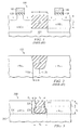
- To manufacture CMOS transistors typically, for example, a workpiece 102 or substrate is implanted with dopants to form the p well and n well.
- An isolation region often referred to in the art as a shallow trench isolation (STI) region 104 is formed between the n well and p well of the PMOS transistor and the NMOS transistor.
- STI shallow trench isolation
- the STI region 104 has a width W and a depth D within the workpiece 102.
- the STI region usually extends within the workpiece 102 by about the depth of the maximum n well and p well doping concentration, e.g., about 0.5 to 1.0 ⁇ m, for example.
- a gate dielectric material 106 is deposited over the workpiece 102 and the STI region 104, and a gate material 108 is deposited over the gate dielectric material 106.
- the gate material 108 and the gate dielectric material 106 are patterned using lithography to form the gate and gate dielectric of the PMOS and NMOS transistors. Dopants are then implanted into the top surface of the p well and n well to form n type and p type source and drain regions of the transistors, for example.
- Sidewall spacers may be formed over the sidewalls of the gates 108 and gate dielectric 106, and other processing steps may be continued (not shown) to complete the fabrication of the CMOS device 100, such as the deposition of insulating layers and the formation of contacts to make electrical contact to portions of the PMOS and NMOS transistors.
- the STI region 104 separates the p well from the n well. Because the p well and n well are implanted, they have a maximum dopant concentration at a certain depth within the workpiece 102. The trench for the STI region 104 should extend down to the maximum well dopant concentration. The breakdown voltage is reached when the depletion zone beginning in the source/drain (SD) regions from the one well (e.g., a p-SD for an n well and an n-SD for a p well) reaches the adjacent well.
- SD source/drain
- the depletion zone grows only slightly at a high dopant concentration, e.g., around the bottom of the STI region 104 trench. Therefore, the width of the STI bottom region is most important for the isolation performance of the STI region. The bottom of the STI region 104 trench should therefore be wide enough to assure that a sufficiently large voltage can be applied across both wells, without punch-through of the depletion zone.
- STI regions 104 Another problem with prior art STI regions 104 is that the deeper the p well and n well are, the deeper the STI regions 104 need to be. Forming deeper trenches for the STI region 104 requires a thicker layer of photoresist for the mask for the implantation process, making it difficult to scale the CMOS device 100 or reduce the size.
- misalignment due to unavoidable overlay tolerances in the lithographic process can result when the STI region 104 is formed, resulting in an STI region 104 that is not immediately disposed between or centered at the junction 1 10a of the p well and n well, as shown in Figure 2.
- the STI region 104 trench may be centered around a point 110b (e.g., within the n well, in Figure 2) that is offset from the desired junction 110a of the p well and n well by an amount X. This misalignment causes device 100 failures, for example.
- STI regions are formed that have a retrograde shape, being wider at the bottom and narrower at the top.
- a method of forming an isolation structure for a semiconductor device includes providing a workpiece, and exposing the workpiece to a first etch process to form a first trench portion in the workpiece.
- the first etch process comprises a first bias power level, and the first trench portion has a first width.
- the workpiece is exposed to a second etch process to form a second trench portion beneath the first trench portion in the workpiece.
- the second etch process comprises a second bias power level, and the second trench portion has a second width.
- the second bias power level is greater than the first bias power level, and the second width is greater than the first width.
- the first trench portion and the second trench portion are filled with an insulating material.
- a method of forming an isolation structure for a semiconductor device includes providing a workpiece, and exposing the workpiece to a first etch process to form a first trench portion in the workpiece.
- the first trench portion has a first width.
- a protective liner is formed on the first trench portion, the protective liner comprising a thickness of less than 50 nm.
- the protective liner is removed from at least a bottom surface of the first trench portion.
- the workpiece is exposed to a second etch process to form a second trench portion beneath the first trench portion in the workpiece.
- the second trench portion has a second width, and the second width is greater than the first width.
- the first trench portion and the second trench portion are then filled with an insulating material.
- a method of forming an isolation structure for a semiconductor device includes providing a workpiece, and exposing the workpiece to a first process to form a first trench portion in the workpiece, the first trench portion having a first width, the first process comprising a first etch process.
- a protective liner is formed on the first trench portion, the protective liner comprising a nitride, a carbon-containing material, or a polymer.
- the protective liner is removed from at least a bottom surface of the first trench portion.
- the workpiece is exposed to a second process to form a second trench portion beneath the first trench portion in the workpiece.
- the second trench portion has a second width, the second width being greater than the first width. At least the first trench portion is then filled with an insulating material.
- a semiconductor device in accordance with another preferred embodiment of the present invention, includes a workpiece, the workpiece having a top surface, and an isolation region formed within the workpiece.
- the isolation region includes a first portion proximate the top surface of the workpiece, the first portion having a first width and comprising sidewalls.
- the isolation region includes a second portion disposed beneath the first portion, the second portion having a second width, the second width being greater than the first width.
- the isolation region includes an insulating material disposed within the first trench portion and the second trench portion, wherein a liner does not reside along sidewalls of the first trench portion, between the insulating material and the workpiece.
- Advantages of preferred embodiments of the present invention include providing novel methods of forming and structures for STI regions.
- the STI regions are wider at the bottom than at the top, yet because the optional protective liner on the sidewalls of the upper first portion is very thin, the trenches are easily filled with insulating material, resulting in a void-free fill.
- voids may form in the lower part, but not the upper part of the trench in the fill process for the trenches.
- the novel STI regions may be scaled to a smaller size, allowing further reduction in the size of semiconductor devices.
- Figure 1 shows a cross-sectional view of a prior art CMOS device having an STI region formed between a PMOS and an NMOS transistor;
- Figure 2 illustrates the misalignment problems that can occur in prior art STI formation
- Figure 3 shows a novel STI region having a retrograde shape, in accordance with an embodiment of the present invention
- Figures 4 through 6 and 7A show cross-sectional views of a semiconductor device at various stages of manufacturing in accordance with a preferred embodiment of the present invention, wherein an STI region is formed using a two step etch process;
- Figure 7B shows an optional liner that may be formed within the STI region trench, before filling the trench with insulating material, and voids that may form in the lower part of the trench;
- Figures 8 through 10 show another preferred method of forming STI regions in accordance with an embodiment of the present invention, wherein a protective liner is formed in a top region of the trench;
- Figures 11 through 13 show another preferred method of forming STI regions in accordance with an embodiment of the present invention, wherein a local oxidation process is used to widen the bottom of the trench while the upper part of the trench is protected by a nitride liner; and
- Figures 14 through 17 show yet another preferred method of forming STI regions in accordance with an embodiment of the present invention, wherein, after forming the protecting nitride liner, an etch process is used to deepen the trench.
- the present invention will be described with respect to preferred embodiments in a specific context, namely, in the formation of STI regions for CMOS transistors.
- the invention may also be applied, however, to other isolation structures and methods of forming thereof for semiconductor devices.
- Embodiments of the present invention include novel, improved methods of forming STI regions that are thinner at the top and wider at the bottom.
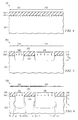
- a novel STI region 222/224 for a semiconductor device 200 in accordance with an embodiment of the present invention is shown in a cross-sectional view.
- An STI region 222/224 is formed in a semiconductor workpiece 202 having a top surface.
- the STI or isolation region 222/224 includes a first portion 226 proximate the top surface of the workpiece 202, the first portion 226 having a first width d 1 and comprising sidewalls.
- the first portion 226 extends into the workpiece 202 by a distance d 2 .
- the isolation region 222/224 includes a second portion 228 disposed beneath the first portion 226, the second portion 228 having a second width d 4 , the second width d 4 being greater than the first width d 1 .
- the second portion 228 is preferably wider than the first portion 226 on each side by a distance d 3 , as shown.
- the second portion 228 extends beneath the first portion 226 by a distance d 5 .
- the STI region 222/224 extends to a point 230 within the workpiece 202, as shown, and may be formed between a p well and an n well of a CMOS device, as shown, as an example, although the STI region 222/224 may alternatively be formed in other devices or components of a semiconductor device 200, e.g., between one n-well or one p-well.
- the STI region 222/224 is filled with an insulating material 224 such as silicon dioxide.
- the first width d 1 preferably comprises about 100 nm or less
- the second width d 4 preferably comprises about 150 nm or less, as examples, although alternatively, the first width d 1 and second width d 4 may comprise other dimensions, e.g., they may be larger.
- the first width d 1 and second width d 4 may be scaled to smaller dimensions, in accordance with embodiments of the present invention, due to the retrograde shape of the STI region 222/224.
- the first width d 1 and the second width d 2 may be greater than 200 nm, for example.
- the distance d 3 that the second portion 228 is preferably wider at each side than the first portion 226, is preferably about 20 nm or greater, for example.
- the distance d 2 may comprise about 200 nm or less, and the distance d 5 may comprise about 200 nm or less, for example.
- the distance d 2 preferably comprises about half the total depth d 2 + d 5 of the trench for the STI region 222/224.
- d 1 , d 2 , d 3 , d 4 , and d 5 may comprise other dimensions, for example.
- the depth of the second portion 228, distance d 5 may be smaller than the depth of the first portion 226, distance d 2 , in some embodiments.
- the STI region 222/224 may include an optional liner 222 formed on the sidewalls and bottom surface of a trench comprising the first portion 226 and the second portion 228 of the STI region.
- the STI region 222/224 may also include an optional liner formed on the sidewalls of the first portion 226 but not on the second portion 228 (not shown in Figure 3; see Figure 10 at 460).
- the optional liner 460 preferably comprises a thickness of less than about 50 nm, and more preferably comprises a thickness of less than about 25 nm.
- the optional liner 460 may comprise a polymer, SiO 2 , Si x N y , SiC, or combinations or multiple layers thereof, to be described further herein.
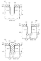
- FIGS 4 through 6 and 7A show cross-sectional views of a semiconductor device 300 at various stages of manufacturing in accordance with a preferred embodiment of the present invention, wherein an STI region 352 or 354 is formed using a two step etch process.
- a workpiece 302 is provided.
- the workpiece 302 may include a semiconductor substrate comprising silicon or other semiconductor materials covered by an insulating layer, for example.
- the workpiece 302 may also include other active components or circuits, not shown.
- the workpiece 302 may comprise silicon oxide over single-crystal silicon, for example.
- the workpiece 302 may include other conductive layers or other semiconductor elements, e.g., transistors, diodes, etc.
- the workpiece 302 may also comprise bulk Si, SiGe, Ge, SiC, or a silicon-on-insulator (SOI) substrate, as examples.
- SOI silicon-on-insulator
- a pad oxide 340 is formed over the workpiece 302.
- the pad oxide 340 may comprise about 4 nm of silicon dioxide (SiO 2 ), for example, although the pad oxide 340 may alternatively comprise other materials and dimensions.
- a pad nitride 342 is formed over the pad oxide 340.
- the pad nitride 342 may comprise about 100 nm of silicon nitride (Si x N y ), for example, although the pad nitride 342 may alternatively comprise other materials and dimensions.
- the semiconductor device 300 may comprise a first region 344 and a second region 346, for example, wherein the first region 344 comprises a region where narrow STI regions will be formed, and wherein the second region 346 comprises a region where wider STI regions will be formed, for example.
- STI regions in the first region 344 may comprise a width of about 80 nm or less
- STI regions in the second region 346 may comprise a width of about 500 nm or greater.
- STI regions comprising a single width, or more than one single width as well as continuous widths may be formed across a surface of the semiconductor device 300, for example.
- the workpiece 302 is exposed to a first etch process 348 to form a first trench portion in the workpiece, as shown in Figure 5.
- a photoresist and/or hard mask may be deposited over the top surface of the pad nitride 342 and patterned with the desired pattern for the STI regions, for example, using lithography.
- the first etch process 348 preferably comprises a reactive ion etch (RIE) that is adapted to etch the workpiece 302, e.g., silicon.
- RIE reactive ion etch
- the first etch process 348 is preferably anisotropic, e.g., it is preferably etches directionally preferentially normal to the top surface of the workpiece 302.
- the first etch process 348 is continued for a predetermined period of time to etch the workpiece 302 by a predetermined amount or distance d 2 .
- the first etch process 348 preferably comprises a first bias power level, and the first trench portion preferably comprises a first width.
- the workpiece 302 is exposed to a second etch process 350 (e.g., with the photoresist and/or hard mask, not shown, still left residing over the pad nitride 342), as shown in Figure 6, to form a second trench portion beneath the first trench portion in the workpiece 302.
- the second etch process 350 preferably an isotropic etch, e.g., it etches in a non-preferential direction.
- a bias power level is selected for the second etch process 350 that does not result in a substantial amount of etching of the sidewalls of the upper, first trench portion.
- the second etch process preferably comprises a second bias power level, wherein the second bias power level is greater than the first bias power level.
- the second trench portion has a second width, wherein the second width is greater than the first width of the first trench portion.
- the first etch process 348 results in the formation of a thin protective liner (not shown in Figure 6; see Figures 9 and 10) on the sidewalls of the upper, first trench portion, wherein the thin protective liner comprises a polymer.
- the thin protective liner may comprise a silicon polymer that is produced as a result of the first etch process 348, for example.
- the optional thin protective liner assists in preventing the sidewalls of the first trench portion from being etched during the second etch process 350, for example.
- the first trench portion and the second trench portion are filled with an insulating material 352, as shown in Figure 7A, or insulating material 354, as shown in Figure 7B.
- the fill process may comprise depositing a spin-on-glass (SOG) 352, as shown in Figure 7A, as one example.
- the fill process may comprise a conformal deposition of an insulator such as tetra ethyl oxysilane (TEOS), using a high aspect ratio fill process (such as HARP TM by Applied Materials, Inc.) 354, as shown in Figure 7B.
- TEOS tetra ethyl oxysilane
- HARP TM high aspect ratio fill process
- other processes and insulating materials may be used to fill the first trench portion and the second trench portion.
- the insulating material 352 preferably comprises a dielectric material typically used for STI in semiconductor devices, for example, such as silicon dioxide. If a conformal fill like HARP TM is used to fill the STI regions, voids 356 may form in the second trench portions, as shown in Figure 7B. Advantageously, the voids 356 form in the lower part of the STI trench, where the voids do not affect the isolation properties, e.g., by forming shorts.
- the protective liner does not impede the filling of the trenches with the insulating material 352 or 354, in accordance with preferred embodiments of the present invention.
- a protective liner comprising a polymer that may be formed during the etch process may be removed in subsequent cleaning steps, for example.
- protective liners comprising silicon oxide or nitride materials may be removed prior to the trench fill process, so that the protective liners will not affect the fill process at all, for example.
- the first etch process 348 may comprise a first source power level
- the second etch process 350 may comprise a second source power level, wherein the second source power level is greater than the first source power level, for example.
- the first source power level of the first etch process 348 may comprise in the range of about 100 to 300 watts, e.g., about 300 watts or less, using a dual plasma source (DPS) plasma etch process
- the second source power level of the second etch process 350 may be in the range of about 500 to 800 watts, e.g., about 500 watts or greater, using a DPS etch process, as examples, although alternatively, other source power levels may be used for the first and second etch processes 348 and 350.
- the first etch process 348 preferably comprises a first pressure
- the second etch process 350 comprises a second pressure, wherein the second pressure is greater than the first pressure.
- the first pressure may comprise in the range of about 5 to 20 milliTorr (mT), e.g., about 20 mT or less
- the second pressure may comprise in the range of about 50 to 80 mT, e.g., about 50 mT or greater, although alternatively, other pressure levels may be used.
- the first etch process 348 comprises a first bias power level
- the second etch process 350 comprises a second bias power level, wherein the second bias power level is greater than the first bias power level.
- the first bias power level may comprise a low bias power (BP) of about 50 watts or less
- the second bias power level may comprise a higher BP of about 200 watts or greater, although alternatively, other bias power levels may be used for the first and second etch processes 348 and 350.
- Figure 7B also shows an optional liner 322 that may be formed within the STI region trench, before filling the trench with insulating material.
- the liner may comprise about 5 to 10 nm of SiO 2 , although alternatively, other materials may be used.
- the optional liner 322 may be used to repair the sidewalls of the workpiece 302 after the first and second etch processes, for example.
- Figures 8 through 10 show another preferred method of forming STI regions in accordance with an embodiment of the present invention, wherein a protective liner 460 is formed in a top region of the trench.
- a protective liner 460 is formed in a top region of the trench.
- Like numerals are used in Figures 8 through 10 as were used in the previous figures.
- a thin protective liner 460 is deposited on the workpiece 402.
- the thin protective liner 460 protects the sidewalls of the first trench portion during the second etch process 466, as shown in Figure 10.
- the liner 460 preferably comprises SiO 2 , Si x N y , SiC, or combinations or multiple layers thereof. More preferably, in some embodiments, the liner 460 comprises Si x N y or SiC, which are materials that provide good protection for a silicon substrate such as workpiece 402 during the second etch process.
- the liner 460 is preferably conformal, and is deposited evenly over the top surface of the pad nitride 442, sidewalls of the pad nitride 442, pad oxide 440, and workpiece 402, and over the bottom surface of the first trench portion, as shown in Figure 8.
- the liner 460 may be formed by chemical vapor deposition (CVD), for example.
- the liner 460 is preferably thin enough that its presence on the sidewalls of the workpiece 402 in the first trench portion will not impede the later manufacturing step of filling the trench.
- the liner 460 is preferably less than 50 nm in thickness. More preferably, the liner 460 comprises a thickness of about 25 nm or less, and most preferably, the liner 460 comprises a thickness of 10 nm or less, as examples, although alternatively, the liner 460 may comprise other dimensions.
- the liner 460 is anisotropically etched to remove the liner 460 from the bottom surface 462 of the first trench portion, leaving the structure shown in Figure 9. Note that the liner 460 may also be removed from the top surface 464 of the pad nitride 442 (not shown).
- the second etch process 466 is used to form the second trench portion that is wider than the first trench portion beneath the first trench portion, as shown in Figure 10. The trenches are then filled, as described with reference to Figures 7A and 7B.
- the liner 460 is not deposited in a separate deposition step, but rather, the liner 460 forms during the first etch process 348, as shown in Figure 9. This occurs as by-products of the first etch process 348 form and deposit on the sidewalls of the first trench portion.
- the liner 460 comprises a polymer comprised of the silicon from the workpiece 402, materials used in the first etch process 348, and possibly also debris, solvents, and/or particulates residing on the workpiece 402 or in the chamber the etch process 348 takes place in, as examples.
- a first etch process 348 may be selected and tuned to achieve the formation of the liner 460, for example.
- the liner 460 is not formed, either intentionally or as a result of the first etch process 348.
- the first etch process parameters are selected and tuned to minimize removal or etching of the sidewalls of the first trench portion during the second etch process 350 (see Figure 6), for example.
- a break-through etch process was used to open or pattern the pad oxide 340 and pad nitride 342.
- the break-through etch process was performed at less than about 12 mT, using a source power of about 300 or less, at about 150 watts BP or less, and using CF 4 , for about 10 seconds or less.
- the first etch process 348 (see Figure 5) comprised a pressure of about 20 mT or less, with about 300 watts or less source power, at about 50 watts or less BP, using HeO 2 and HBR.
- the second etch process 350 (see Figure 6) comprised a pressure of about 50 mT or greater, with about 500 watts or greater source power, at about 200 watts BP or less, using HeO 2 and CF 4 . No additional deposition steps were required to form a liner; the upper first trench portions were protected by a polymer that formed during the first etch process 348.
- An STI trench structure having rounded bottom portions was achieved, having top portions with a width of about 160 to 190 nm, and having bottom portions with a width of about 175 to 200 nm, as examples.
- Figures 11 through 13 show another preferred method of forming STI regions in accordance with an embodiment of the present invention, wherein a local oxidation process is used to widen the bottom of the trench for the STI region while the upper part of the trench is protected by a nitride liner.
- a first etch process such as etch process 348 in Figure 5 is used to form a first portion of the STI trench.
- the first portion of the trench formed by the first etch process 348 preferably forms a trench first portion that comprises a distance d 6 that is equivalent of almost the entire desired depth of the trench for the STI region.
- the first portion of the trench formed by the first etch process 348 may comprise a distance d 6 that is about 3 ⁇ 4 or greater, and more preferably about 7/8 or greater, of the entire trench depth (e.g., (distance d 6 + distance d 7 ) shown in Figures 12 and 13).
- the distance d 6 may comprise about 300 nm or greater, as an example, although other dimensions may be used.
- a thin oxide liner 570 is formed on the sidewalls and bottom surface of the first portion of the trench, as shown in Figure 11.
- the thin oxide liner 570 may be formed by furnace oxidation or rapid thermal oxidation (RTO), as examples, although other methods may alternatively be used.
- the thin oxide liner 570 preferably comprises a thickness of about 5 nm or less, for example, although the thin oxide liner 570 may alternatively comprise other dimensions.
- a thin protective liner 560 is formed over the thin oxide liner 570.
- the thin protective liner 560 preferably comprises the same materials and dimensions as described for thin protective liner 460 in Figures 8 through 10, for example, and in one embodiment preferably comprises a nitride.
- the thin protective liner 560 is anisotropically etched to remove the liner 560 from the bottom surface of the first trench portion, leaving the structure shown in Figure 11 with the thin oxide liner 570 at the bottom of the first trench portion exposed.
- the liner 560 may also be removed from the top surface of the pad nitride 542, as shown.
- the workpiece 502 is exposed to an oxidation process 572, as shown in Figure 11, to cause the thin oxide liner 570 to thicken in the bottom portion of the trench, as shown in Figure 12.
- the workpiece 502 may be exposed to a LOCal Oxidation of Silicon (LOCOS) process to cause oxide growth at the bottom of the first portion of the trench, forming a second portion of the trench beneath the first portion of the trench that is filled with an oxide (e.g., such as SiO 2 .)
- LOCS LOCal Oxidation of Silicon
- the workpiece 502 may be exposed to a furnace oxidation, e.g., in a furnace in the presence of an oxygen-containing gas, at a temperature of about 900 degrees C for a time period of about 60 minutes, as examples, although other ambient parameters may alternatively be used.
- the distance d 7 comprising the thickness of the second portion of the trench that is filled with the oxide preferably comprises about 30 nm or greater, as an example, although distance d 7 may alternatively comprise other dimensions.
- the LOCOS process also causes oxidation in the lateral direction, e.g., by a distance d 8 , which may comprise about 30 mn or greater, for example.
- the thin protective liner 560 preferably comprises a material such as a nitride that will not oxidize during the LOCOS process, for example, preventing the upper, first portion of the trench from filling with oxide material, and providing a better, more even, void-free fill for the STI region.
- Figures 14 through 17 show yet another preferred method of forming STI regions in accordance with an embodiment of the present invention. Like numerals are used in Figures 14 through 17 as were used in the previous figures.
- an etch process such as a RIE is used to deepen the trench by a distance d 10 , as shown in Figure 15, prior to oxidizing the lower part of the trench, as shown in Figure 16.
- the upper first portion of the trench for the STI region comprises a distance d 9 beneath the top surface of the workpiece 602, wherein the distance d 9 preferably comprises about 2/3 or greater of the full trench depth (e.g., the total of distances (d 9 + d 10 + d 11 ) in Figures 16 and 17).
- the etch process removes the oxide liner 670 in the bottom of the first portion of the trench and deepens the trench by a distance d 10 , as shown in Figure 15.
- An oxidation process such as the one described with reference to Figure 12 is then used to oxidize the unprotected bottom portion of the trench, e.g., the bottom portion of the trench not protected by liner 670.
- the oxidation process causes the portion of the trench beneath the first portion protected by the liner 670 to both fill with oxide 674 and form the oxide 674 laterally by a distance d 12 and vertically in a downward direction within the workpiece 602 by a distance d 11 , as shown in Figure 16.
- the distance d 9 is preferably about 300 nm or less
- distance d 10 is preferably about 50 nm or greater
- distances d 11 and d 12 are preferably about 30 nm or greater, as examples, although alternatively distances d 9 , d 10 , d 11 , and d 12 may comprise other dimensions. Deepening the trench before the oxidation process makes the lateral oxidation process more effective, for example.
- the upper portion of the trench is filled with an insulating material 652/654, as described as described with reference to Figures 7A and 7B.
- the oxidation process for the lower, second portion of the trench substantially fills the lower, second portion, thus making it easier to fill the upper, first portion of the trench without void formation, for example.
- Advantages of embodiments of the invention include providing novel methods of forming STI regions 222/224 (Figure 3), 352 (Figure 7A), 354 (Figure 7B), 552/554/574 (Figure 13), and 652/654/674 ( Figure 17) of semiconductor devices 200, 300, 400, 500, and 600.
- the STI regions 222/224, 352, 354, 552/554/574, and 652/654/674 are wider at the bottom than the top, yet because the optional protective liner 460, 560, and 660 on the sidewalls of the upper first portion is very thin, the trenches for the STI regions are easily filled with insulating material, resulting in a void-free fill.
- voids may form in the lower part, but not the upper part of the trench.
- the protective liner 460, 560, and 660 is removed before filling the STI regions, further making the STI region trenches easier to fill, for example.
- the shape of the STI regions 222/224, 352, 354, 552/554/574, and 652/654/674 allows a further reduction in semiconductor device size. Active regions proximate the upper surface of the workpiece 202, 302, 402, 502, and 602 may be placed closer together, while in the lower regions, the wider regions of insulating material in the lower second portion of the trench provide improved isolation.
Landscapes
- Element Separation (AREA)
- Metal-Oxide And Bipolar Metal-Oxide Semiconductor Integrated Circuits (AREA)
- Drying Of Semiconductors (AREA)
Priority Applications (1)
| Application Number | Priority Date | Filing Date | Title |
|---|---|---|---|
| EP12154603A EP2463895A1 (fr) | 2005-09-09 | 2006-09-06 | Isolation pour dispositifs semi-conducteurs |
Applications Claiming Priority (1)
| Application Number | Priority Date | Filing Date | Title |
|---|---|---|---|
| US11/223,232 US20070059897A1 (en) | 2005-09-09 | 2005-09-09 | Isolation for semiconductor devices |
Publications (2)
| Publication Number | Publication Date |
|---|---|
| EP1763074A2 true EP1763074A2 (fr) | 2007-03-14 |
| EP1763074A3 EP1763074A3 (fr) | 2011-06-01 |
Family
ID=37596318
Family Applications (2)
| Application Number | Title | Priority Date | Filing Date |
|---|---|---|---|
| EP12154603A Withdrawn EP2463895A1 (fr) | 2005-09-09 | 2006-09-06 | Isolation pour dispositifs semi-conducteurs |
| EP06120203A Withdrawn EP1763074A3 (fr) | 2005-09-09 | 2006-09-06 | Isolation pour dispositifs semi-conducteurs |
Family Applications Before (1)
| Application Number | Title | Priority Date | Filing Date |
|---|---|---|---|
| EP12154603A Withdrawn EP2463895A1 (fr) | 2005-09-09 | 2006-09-06 | Isolation pour dispositifs semi-conducteurs |
Country Status (4)
| Country | Link |
|---|---|
| US (1) | US20070059897A1 (fr) |
| EP (2) | EP2463895A1 (fr) |
| JP (2) | JP2007110096A (fr) |
| TW (1) | TW200711036A (fr) |
Cited By (3)
| Publication number | Priority date | Publication date | Assignee | Title |
|---|---|---|---|---|
| CN103094286A (zh) * | 2011-11-08 | 2013-05-08 | 上海华虹Nec电子有限公司 | 浅槽隔离结构及其进行离子注入的方法 |
| CN110098208A (zh) * | 2017-04-03 | 2019-08-06 | 豪威科技股份有限公司 | 制作像素阵列的方法 |
| US20230395653A1 (en) * | 2022-06-07 | 2023-12-07 | International Business Machines Corporation | Reduced n-well and p-well spacing |
Families Citing this family (28)
| Publication number | Priority date | Publication date | Assignee | Title |
|---|---|---|---|---|
| US20070235783A9 (en) * | 2005-07-19 | 2007-10-11 | Micron Technology, Inc. | Semiconductor constructions, memory arrays, electronic systems, and methods of forming semiconductor constructions |
| US7772672B2 (en) | 2005-09-01 | 2010-08-10 | Micron Technology, Inc. | Semiconductor constructions |
| KR100772709B1 (ko) * | 2005-12-13 | 2007-11-02 | 주식회사 하이닉스반도체 | 반도체 소자의 소자분리막 제조방법 |
| TWI278067B (en) * | 2006-01-09 | 2007-04-01 | Nanya Technology Corp | Method for fabricating a recessed-gate MOS transistor device |
| KR100689514B1 (ko) * | 2006-01-23 | 2007-03-02 | 주식회사 하이닉스반도체 | 반도체 소자 및 그의 제조 방법 |
| TWI309067B (en) * | 2006-03-15 | 2009-04-21 | Nanya Technology Corp | Method for fabricating a recessed-gate mos transistor device |
| US7799694B2 (en) * | 2006-04-11 | 2010-09-21 | Micron Technology, Inc. | Methods of forming semiconductor constructions |
| US7601607B2 (en) * | 2006-05-15 | 2009-10-13 | Chartered Semiconductor Manufacturing, Ltd. | Protruded contact and insertion of inter-layer-dielectric material to match damascene hardmask to improve undercut for low-k interconnects |
| US7709320B2 (en) * | 2006-06-28 | 2010-05-04 | International Business Machines Corporation | Method of fabricating trench capacitors and memory cells using trench capacitors |
| KR100745934B1 (ko) * | 2006-06-30 | 2007-08-02 | 주식회사 하이닉스반도체 | 반도체 소자 및 그의 형성 방법 |
| US7858476B2 (en) * | 2006-10-30 | 2010-12-28 | Hynix Semiconductor Inc. | Method for fabricating semiconductor device with recess gate |
| KR100827538B1 (ko) * | 2006-12-28 | 2008-05-06 | 주식회사 하이닉스반도체 | 반도체 소자 및 그 제조 방법 |
| US7723818B2 (en) * | 2007-05-22 | 2010-05-25 | Infineon Technologies Ag | Semiconductor devices and methods of manufacture thereof |
| US8125037B2 (en) | 2008-08-12 | 2012-02-28 | International Business Machines Corporation | Field effect transistor with channel region edge and center portions having different band structures for suppressed corner leakage |
| US7838353B2 (en) * | 2008-08-12 | 2010-11-23 | International Business Machines Corporation | Field effect transistor with suppressed corner leakage through channel material band-edge modulation, design structure and method |
| JP2010153598A (ja) * | 2008-12-25 | 2010-07-08 | Sharp Corp | 半導体装置及びその製造方法 |
| CN102468213B (zh) * | 2010-11-19 | 2014-10-01 | 中国科学院微电子研究所 | 沟槽隔离结构及其形成方法 |
| US8525188B2 (en) | 2010-11-19 | 2013-09-03 | Institute of Microelectronics, Chinese Academy of Sciences | Shallow trench isolation structure and method for forming the same |
| CN102694007B (zh) * | 2011-03-22 | 2014-11-19 | 中国科学院微电子研究所 | 半导体结构及其制造方法 |
| US20130187159A1 (en) | 2012-01-23 | 2013-07-25 | Infineon Technologies Ag | Integrated circuit and method of forming an integrated circuit |
| US8927387B2 (en) * | 2012-04-09 | 2015-01-06 | International Business Machines Corporation | Robust isolation for thin-box ETSOI MOSFETS |
| US9646871B2 (en) * | 2014-07-22 | 2017-05-09 | Taiwan Semiconductor Manufacturing Company Ltd. | Semiconductor structure with shallow trench isolation and manufacturing method thereof |
| CN104658914B (zh) * | 2015-02-15 | 2018-10-26 | 上海华虹宏力半导体制造有限公司 | 一种改善形貌的深沟槽制造方法及深沟槽 |
| CN109585293B (zh) * | 2017-09-29 | 2021-12-24 | 台湾积体电路制造股份有限公司 | 切割金属工艺中的基脚去除 |
| US10453738B2 (en) * | 2017-12-22 | 2019-10-22 | Texas Instruments Incorporated | Selective etches for reducing cone formation in shallow trench isolations |
| KR102420163B1 (ko) * | 2018-01-18 | 2022-07-12 | 삼성전자주식회사 | 집적회로 소자 및 그 제조 방법 |
| CN116031157A (zh) * | 2022-11-29 | 2023-04-28 | 华虹半导体(无锡)有限公司 | 悬梁结构的形成方法 |
| DE102023210487A1 (de) * | 2023-10-24 | 2025-04-24 | Fraunhofer-Gesellschaft zur Förderung der angewandten Forschung eingetragener Verein | Verfahren zum Herstellen eines Boden-Oxids |
Citations (7)
| Publication number | Priority date | Publication date | Assignee | Title |
|---|---|---|---|---|
| EP0256311A2 (fr) | 1986-08-09 | 1988-02-24 | International Business Machines Corporation | Procédé RIE pour graver des rainures d'isolation à parois verticales dans du silicium et du polycide |
| WO1999067817A1 (fr) | 1998-06-22 | 1999-12-29 | Applied Materials, Inc. | Gravure de tranchees de silicium par des precurseurs contenant du silicium afin de diminuer ou d'eviter l'erosion du masque |
| US6110798A (en) * | 1996-01-05 | 2000-08-29 | Micron Technology, Inc. | Method of fabricating an isolation structure on a semiconductor substrate |
| EP1043769A1 (fr) | 1999-04-07 | 2000-10-11 | STMicroelectronics S.r.l. | Procédé pour la production d'une plaquette en matériau semi-conducteur comportant des régions monocristallines séparées par des régions de materiau isolant, notamment pour la fabrication de dispositifs de puissance intégrés, et plaquette ainsi obtenue |
| US6376286B1 (en) | 1999-10-20 | 2002-04-23 | Advanced Micro Devices, Inc. | Field effect transistor with non-floating body and method for forming same on a bulk silicon wafer |
| WO2002073668A2 (fr) | 2001-03-13 | 2002-09-19 | Infineon Technologies Ag | Procede servant a creer une tranchee profonde presentant un profil et une surface ameliores |
| US20040110383A1 (en) | 2002-12-05 | 2004-06-10 | Hiroyuki Tanaka | Method of forming device isolation trench |
Family Cites Families (17)
| Publication number | Priority date | Publication date | Assignee | Title |
|---|---|---|---|---|
| JPS5743438A (en) * | 1980-08-29 | 1982-03-11 | Toshiba Corp | Semiconductor device and manufacture thereof |
| JPS60150644A (ja) * | 1984-01-18 | 1985-08-08 | Toshiba Corp | 相補型半導体装置及びその製造方法 |
| JPS63151047A (ja) * | 1986-12-16 | 1988-06-23 | Matsushita Electric Ind Co Ltd | Mos型半導体装置の製造方法 |
| DE3809218C2 (de) * | 1987-03-20 | 1994-09-01 | Mitsubishi Electric Corp | Halbleitereinrichtung mit einem Graben und Verfahren zum Herstellen einer solchen Halbleitereinrichtung |
| EP0540262A2 (fr) * | 1991-10-31 | 1993-05-05 | STMicroelectronics, Inc. | Isolation à ramure |
| US5498566A (en) * | 1993-11-15 | 1996-03-12 | Lg Semicon Co., Ltd. | Isolation region structure of semiconductor device and method for fabricating the same |
| US5963789A (en) * | 1996-07-08 | 1999-10-05 | Kabushiki Kaisha Toshiba | Method for silicon island formation |
| US7045468B2 (en) * | 1999-04-09 | 2006-05-16 | Intel Corporation | Isolated junction structure and method of manufacture |
| US6251750B1 (en) * | 1999-09-15 | 2001-06-26 | United Microelectronics Corp. | Method for manufacturing shallow trench isolation |
| US6071823A (en) * | 1999-09-21 | 2000-06-06 | Promos Technology, Inc | Deep trench bottle-shaped etch in centura mark II NG |
| US6833079B1 (en) * | 2000-02-17 | 2004-12-21 | Applied Materials Inc. | Method of etching a shaped cavity |
| JP4200626B2 (ja) * | 2000-02-28 | 2008-12-24 | 株式会社デンソー | 絶縁ゲート型パワー素子の製造方法 |
| JP2002043413A (ja) * | 2000-07-25 | 2002-02-08 | Toshiba Corp | 半導体装置及び半導体装置の製造方法 |
| US6313008B1 (en) * | 2001-01-25 | 2001-11-06 | Chartered Semiconductor Manufacturing Inc. | Method to form a balloon shaped STI using a micro machining technique to remove heavily doped silicon |
| US6825086B2 (en) * | 2003-01-17 | 2004-11-30 | Sharp Laboratories Of America, Inc. | Strained-silicon channel CMOS with sacrificial shallow trench isolation oxide liner |
| KR100525797B1 (ko) * | 2003-06-18 | 2005-11-02 | 동부아남반도체 주식회사 | 소자분리막 구조 및 제조 방법 |
| US7122437B2 (en) * | 2003-12-19 | 2006-10-17 | Infineon Technologies Ag | Deep trench capacitor with buried plate electrode and isolation collar |
-
2005
- 2005-09-09 US US11/223,232 patent/US20070059897A1/en not_active Abandoned
-
2006
- 2006-08-31 TW TW095132251A patent/TW200711036A/zh unknown
- 2006-09-06 EP EP12154603A patent/EP2463895A1/fr not_active Withdrawn
- 2006-09-06 EP EP06120203A patent/EP1763074A3/fr not_active Withdrawn
- 2006-09-11 JP JP2006245921A patent/JP2007110096A/ja active Pending
-
2010
- 2010-11-02 JP JP2010246006A patent/JP5707098B2/ja not_active Expired - Fee Related
Patent Citations (7)
| Publication number | Priority date | Publication date | Assignee | Title |
|---|---|---|---|---|
| EP0256311A2 (fr) | 1986-08-09 | 1988-02-24 | International Business Machines Corporation | Procédé RIE pour graver des rainures d'isolation à parois verticales dans du silicium et du polycide |
| US6110798A (en) * | 1996-01-05 | 2000-08-29 | Micron Technology, Inc. | Method of fabricating an isolation structure on a semiconductor substrate |
| WO1999067817A1 (fr) | 1998-06-22 | 1999-12-29 | Applied Materials, Inc. | Gravure de tranchees de silicium par des precurseurs contenant du silicium afin de diminuer ou d'eviter l'erosion du masque |
| EP1043769A1 (fr) | 1999-04-07 | 2000-10-11 | STMicroelectronics S.r.l. | Procédé pour la production d'une plaquette en matériau semi-conducteur comportant des régions monocristallines séparées par des régions de materiau isolant, notamment pour la fabrication de dispositifs de puissance intégrés, et plaquette ainsi obtenue |
| US6376286B1 (en) | 1999-10-20 | 2002-04-23 | Advanced Micro Devices, Inc. | Field effect transistor with non-floating body and method for forming same on a bulk silicon wafer |
| WO2002073668A2 (fr) | 2001-03-13 | 2002-09-19 | Infineon Technologies Ag | Procede servant a creer une tranchee profonde presentant un profil et une surface ameliores |
| US20040110383A1 (en) | 2002-12-05 | 2004-06-10 | Hiroyuki Tanaka | Method of forming device isolation trench |
Cited By (3)
| Publication number | Priority date | Publication date | Assignee | Title |
|---|---|---|---|---|
| CN103094286A (zh) * | 2011-11-08 | 2013-05-08 | 上海华虹Nec电子有限公司 | 浅槽隔离结构及其进行离子注入的方法 |
| CN110098208A (zh) * | 2017-04-03 | 2019-08-06 | 豪威科技股份有限公司 | 制作像素阵列的方法 |
| US20230395653A1 (en) * | 2022-06-07 | 2023-12-07 | International Business Machines Corporation | Reduced n-well and p-well spacing |
Also Published As
| Publication number | Publication date |
|---|---|
| TW200711036A (en) | 2007-03-16 |
| JP2007110096A (ja) | 2007-04-26 |
| US20070059897A1 (en) | 2007-03-15 |
| EP2463895A1 (fr) | 2012-06-13 |
| JP5707098B2 (ja) | 2015-04-22 |
| JP2011066435A (ja) | 2011-03-31 |
| EP1763074A3 (fr) | 2011-06-01 |
Similar Documents
| Publication | Publication Date | Title |
|---|---|---|
| EP1763074A2 (fr) | Isolation pour dispositifs semi-conducteurs | |
| US7205207B2 (en) | High performance strained CMOS devices | |
| US8502316B2 (en) | Self-aligned two-step STI formation through dummy poly removal | |
| US6087208A (en) | Method for increasing gate capacitance by using both high and low dielectric gate material | |
| JP2007110096A5 (fr) | ||
| CN100505263C (zh) | 半导体结构及其形成方法 | |
| US6881631B2 (en) | Method of manufacturing semiconductor device | |
| KR0165457B1 (ko) | 트렌치 소자분리 방법 | |
| WO1998036452A1 (fr) | Composant a semiconducteur et procede de fabrication | |
| US8410553B2 (en) | Semiconductor structure including high voltage device | |
| EP1145304B1 (fr) | Utilisation d'un élément d'espacement isolant pour éviter roll-off de la tension de seuil dans les dispositifs étroits | |
| US20040195632A1 (en) | Semiconductor device and method of manufacturing the same | |
| KR100742025B1 (ko) | 반도체 디바이스와 그 제조 방법 | |
| US8399956B2 (en) | Semiconductor devices and methods of manufacture thereof | |
| KR100515181B1 (ko) | 반도체 장치의 제조 방법 | |
| US9825030B2 (en) | High quality deep trench oxide | |
| US8017472B2 (en) | CMOS devices having stress-altering material lining the isolation trenches and methods of manufacturing thereof | |
| US6703187B2 (en) | Method of forming a self-aligned twin well structure with a single mask | |
| US6235609B1 (en) | Method for forming isolation areas with improved isolation oxide | |
| US6617216B1 (en) | Quasi-damascene gate, self-aligned source/drain methods for fabricating devices | |
| KR20030001179A (ko) | 반도체 소자의 소자 격리층 형성 방법 | |
| US7223698B1 (en) | Method of forming a semiconductor arrangement with reduced field-to active step height | |
| KR100408862B1 (ko) | 반도체 소자의 소자 분리막 형성 방법 | |
| KR100423094B1 (ko) | 실리사이드의 브릿지 방지방법 | |
| KR100565749B1 (ko) | 반도체 소자의 격리영역 및 그 제조방법 |
Legal Events
| Date | Code | Title | Description |
|---|---|---|---|
| PUAI | Public reference made under article 153(3) epc to a published international application that has entered the european phase |
Free format text: ORIGINAL CODE: 0009012 |
|
| AK | Designated contracting states |
Kind code of ref document: A2 Designated state(s): AT BE BG CH CY CZ DE DK EE ES FI FR GB GR HU IE IS IT LI LT LU LV MC NL PL PT RO SE SI SK TR |
|
| AX | Request for extension of the european patent |
Extension state: AL BA HR MK YU |
|
| RAP1 | Party data changed (applicant data changed or rights of an application transferred) |
Owner name: INFINEON TECHNOLOGIES AG |
|
| PUAL | Search report despatched |
Free format text: ORIGINAL CODE: 0009013 |
|
| AK | Designated contracting states |
Kind code of ref document: A3 Designated state(s): AT BE BG CH CY CZ DE DK EE ES FI FR GB GR HU IE IS IT LI LT LU LV MC NL PL PT RO SE SI SK TR |
|
| AX | Request for extension of the european patent |
Extension state: AL BA HR MK RS |
|
| 17P | Request for examination filed |
Effective date: 20111103 |
|
| AKX | Designation fees paid |
Designated state(s): DE FR |
|
| 17Q | First examination report despatched |
Effective date: 20130215 |
|
| GRAP | Despatch of communication of intention to grant a patent |
Free format text: ORIGINAL CODE: EPIDOSNIGR1 |
|
| INTG | Intention to grant announced |
Effective date: 20171024 |
|
| STAA | Information on the status of an ep patent application or granted ep patent |
Free format text: STATUS: THE APPLICATION IS DEEMED TO BE WITHDRAWN |
|
| 18D | Application deemed to be withdrawn |
Effective date: 20180306 |