EP1763075A1 - Methode für die präzise Vereinzelung von integrierten Schaltungen unter Verwendung von differentiellen Ätzraten - Google Patents
Methode für die präzise Vereinzelung von integrierten Schaltungen unter Verwendung von differentiellen Ätzraten Download PDFInfo
- Publication number
- EP1763075A1 EP1763075A1 EP05108400A EP05108400A EP1763075A1 EP 1763075 A1 EP1763075 A1 EP 1763075A1 EP 05108400 A EP05108400 A EP 05108400A EP 05108400 A EP05108400 A EP 05108400A EP 1763075 A1 EP1763075 A1 EP 1763075A1
- Authority
- EP
- European Patent Office
- Prior art keywords
- etching process
- singulation
- depth
- integrated circuit
- wafer
- Prior art date
- Legal status (The legal status is an assumption and is not a legal conclusion. Google has not performed a legal analysis and makes no representation as to the accuracy of the status listed.)
- Withdrawn
Links
Images


Classifications
-
- H—ELECTRICITY
- H10—SEMICONDUCTOR DEVICES; ELECTRIC SOLID-STATE DEVICES NOT OTHERWISE PROVIDED FOR
- H10F—INORGANIC SEMICONDUCTOR DEVICES SENSITIVE TO INFRARED RADIATION, LIGHT, ELECTROMAGNETIC RADIATION OF SHORTER WAVELENGTH OR CORPUSCULAR RADIATION
- H10F39/00—Integrated devices, or assemblies of multiple devices, comprising at least one element covered by group H10F30/00, e.g. radiation detectors comprising photodiode arrays
- H10F39/011—Manufacture or treatment of image sensors covered by group H10F39/12
-
- H—ELECTRICITY
- H10—SEMICONDUCTOR DEVICES; ELECTRIC SOLID-STATE DEVICES NOT OTHERWISE PROVIDED FOR
- H10P—GENERIC PROCESSES OR APPARATUS FOR THE MANUFACTURE OR TREATMENT OF DEVICES COVERED BY CLASS H10
- H10P54/00—Cutting or separating of wafers, substrates or parts of devices
Definitions
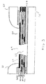
- a predetermined portion 70 of second surface 10 is removed slightly beyond the depth of singulation channel 65, such as by lapping, grinding, polishing or chemical mechanical polishing (CMP) or equivalent processes as are well known in the semiconductor arts.
- CMP chemical mechanical polishing
Landscapes
- Dicing (AREA)
Priority Applications (1)
| Application Number | Priority Date | Filing Date | Title |
|---|---|---|---|
| EP05108400A EP1763075A1 (de) | 2005-09-13 | 2005-09-13 | Methode für die präzise Vereinzelung von integrierten Schaltungen unter Verwendung von differentiellen Ätzraten |
Applications Claiming Priority (1)
| Application Number | Priority Date | Filing Date | Title |
|---|---|---|---|
| EP05108400A EP1763075A1 (de) | 2005-09-13 | 2005-09-13 | Methode für die präzise Vereinzelung von integrierten Schaltungen unter Verwendung von differentiellen Ätzraten |
Publications (1)
| Publication Number | Publication Date |
|---|---|
| EP1763075A1 true EP1763075A1 (de) | 2007-03-14 |
Family
ID=35709008
Family Applications (1)
| Application Number | Title | Priority Date | Filing Date |
|---|---|---|---|
| EP05108400A Withdrawn EP1763075A1 (de) | 2005-09-13 | 2005-09-13 | Methode für die präzise Vereinzelung von integrierten Schaltungen unter Verwendung von differentiellen Ätzraten |
Country Status (1)
| Country | Link |
|---|---|
| EP (1) | EP1763075A1 (de) |
Cited By (4)
| Publication number | Priority date | Publication date | Assignee | Title |
|---|---|---|---|---|
| EP2315248A1 (de) * | 2009-10-26 | 2011-04-27 | Fondazione Bruno Kessler | Verfahren zur Herstellung eines Halbleitersensors und erhaltener Sensor |
| EP2693480A4 (de) * | 2011-03-31 | 2014-10-01 | Hamamatsu Photonics Kk | Lichtdiodenarray-modul und herstellungsverfahren dafür |
| DE102011055224B4 (de) | 2010-11-15 | 2018-09-27 | Infineon Technologies Ag | Verfahren zum Herstellen eines Halbleiterchips und ein Halbleiterchip |
| CN111079281A (zh) * | 2019-12-11 | 2020-04-28 | 北京华大九天软件有限公司 | 一种分割版图并生成随机图形的方法 |
Citations (6)
| Publication number | Priority date | Publication date | Assignee | Title |
|---|---|---|---|---|
| US5259925A (en) | 1992-06-05 | 1993-11-09 | Mcdonnell Douglas Corporation | Method of cleaning a plurality of semiconductor devices |
| DE4241045C1 (de) * | 1992-12-05 | 1994-05-26 | Bosch Gmbh Robert | Verfahren zum anisotropen Ätzen von Silicium |
| US6174789B1 (en) * | 1998-02-20 | 2001-01-16 | Nec Corporation | Method of dividing a compound semiconductor wafer into pellets by utilizing extremely narrow scribe regions |
| US6177352B1 (en) | 1996-08-13 | 2001-01-23 | Siemens Aktiengesellschaft | Method for producing semiconductor bodies with an MOVPE layer sequence |
| EP1394851A2 (de) | 2002-09-02 | 2004-03-03 | Shinko Electric Industries Co. Ltd. | Halbleiterchip und Herstellungsverfahren dafür |
| US6756288B1 (en) * | 1999-07-01 | 2004-06-29 | Fraunhofer-Gesellschaft Zur Foerderung Der Angewandten Forschung E.V. | Method of subdividing a wafer |
-
2005
- 2005-09-13 EP EP05108400A patent/EP1763075A1/de not_active Withdrawn
Patent Citations (6)
| Publication number | Priority date | Publication date | Assignee | Title |
|---|---|---|---|---|
| US5259925A (en) | 1992-06-05 | 1993-11-09 | Mcdonnell Douglas Corporation | Method of cleaning a plurality of semiconductor devices |
| DE4241045C1 (de) * | 1992-12-05 | 1994-05-26 | Bosch Gmbh Robert | Verfahren zum anisotropen Ätzen von Silicium |
| US6177352B1 (en) | 1996-08-13 | 2001-01-23 | Siemens Aktiengesellschaft | Method for producing semiconductor bodies with an MOVPE layer sequence |
| US6174789B1 (en) * | 1998-02-20 | 2001-01-16 | Nec Corporation | Method of dividing a compound semiconductor wafer into pellets by utilizing extremely narrow scribe regions |
| US6756288B1 (en) * | 1999-07-01 | 2004-06-29 | Fraunhofer-Gesellschaft Zur Foerderung Der Angewandten Forschung E.V. | Method of subdividing a wafer |
| EP1394851A2 (de) | 2002-09-02 | 2004-03-03 | Shinko Electric Industries Co. Ltd. | Halbleiterchip und Herstellungsverfahren dafür |
Cited By (5)
| Publication number | Priority date | Publication date | Assignee | Title |
|---|---|---|---|---|
| EP2315248A1 (de) * | 2009-10-26 | 2011-04-27 | Fondazione Bruno Kessler | Verfahren zur Herstellung eines Halbleitersensors und erhaltener Sensor |
| DE102011055224B4 (de) | 2010-11-15 | 2018-09-27 | Infineon Technologies Ag | Verfahren zum Herstellen eines Halbleiterchips und ein Halbleiterchip |
| EP2693480A4 (de) * | 2011-03-31 | 2014-10-01 | Hamamatsu Photonics Kk | Lichtdiodenarray-modul und herstellungsverfahren dafür |
| US9496298B2 (en) | 2011-03-31 | 2016-11-15 | Hamamatsu Photonics K.K. | Photodiode array module and method for manufacturing same |
| CN111079281A (zh) * | 2019-12-11 | 2020-04-28 | 北京华大九天软件有限公司 | 一种分割版图并生成随机图形的方法 |
Similar Documents
| Publication | Publication Date | Title |
|---|---|---|
| USRE43877E1 (en) | Method for precision integrated circuit die singulation using differential etch rates | |
| US6521513B1 (en) | Silicon wafer configuration and method for forming same | |
| CN102354692B (zh) | 晶片和切割晶片的方法 | |
| CN105340064B (zh) | 半导体片制造方法、包括半导体片的电路板和成像设备 | |
| US8962452B2 (en) | Semiconductor die singulation apparatus and method | |
| US9196511B2 (en) | Semiconductor die singulation methods | |
| JP5817905B1 (ja) | 半導体片の製造方法 | |
| US5196378A (en) | Method of fabricating an integrated circuit having active regions near a die edge | |
| US7482251B1 (en) | Etch before grind for semiconductor die singulation | |
| US9589812B2 (en) | Fabrication method of semiconductor piece | |
| US8637967B2 (en) | Method for fabricating a semiconductor chip and semiconductor chip | |
| KR100855015B1 (ko) | 패키징된 집적회로 및 그 제조 방법 | |
| US8030180B2 (en) | Method of manufacturing a semiconductor device | |
| CN104867871B (zh) | 半导体器件及形成其的方法 | |
| US12297105B2 (en) | Semiconductor structure including scribe line structures and method for fabricating the same | |
| US20230274979A1 (en) | Plasma diced wafers and methods thereof | |
| KR101116993B1 (ko) | 집적 회로의 제조 방법 | |
| EP1763075A1 (de) | Methode für die präzise Vereinzelung von integrierten Schaltungen unter Verwendung von differentiellen Ätzraten | |
| US20230178413A1 (en) | Plasma diced wafers and methods thereof | |
| US20170084468A1 (en) | Method for processing a wafer and method for dicing a wafer | |
| US20050124140A1 (en) | Pre-fabrication scribing | |
| KR20070074937A (ko) | 스크라이브 레인의 트렌치를 이용한 반도체 웨이퍼의다이싱 방법 | |
| KR101192526B1 (ko) | 웨이퍼로부터 반도체 칩을 제조하기 위한 방법 및 반도체 구성 요소 | |
| GB2102202A (en) | Semiconductor device passivation | |
| JPS61267343A (ja) | 半導体装置の製造方法 |
Legal Events
| Date | Code | Title | Description |
|---|---|---|---|
| PUAI | Public reference made under article 153(3) epc to a published international application that has entered the european phase |
Free format text: ORIGINAL CODE: 0009012 |
|
| AK | Designated contracting states |
Kind code of ref document: A1 Designated state(s): AT BE BG CH CY CZ DE DK EE ES FI FR GB GR HU IE IS IT LI LT LU LV MC NL PL PT RO SE SI SK TR |
|
| AX | Request for extension of the european patent |
Extension state: AL BA HR MK YU |
|
| 17P | Request for examination filed |
Effective date: 20070824 |
|
| 17Q | First examination report despatched |
Effective date: 20071004 |
|
| AKX | Designation fees paid |
Designated state(s): AT BE BG CH CY CZ DE DK EE ES FI FR GB GR HU IE IS IT LI LT LU LV MC NL PL PT RO SE SI SK TR |
|
| STAA | Information on the status of an ep patent application or granted ep patent |
Free format text: STATUS: THE APPLICATION IS DEEMED TO BE WITHDRAWN |
|
| 18D | Application deemed to be withdrawn |
Effective date: 20100402 |