EP1763130A1 - Schutzschaltung - Google Patents
Schutzschaltung Download PDFInfo
- Publication number
- EP1763130A1 EP1763130A1 EP06018469A EP06018469A EP1763130A1 EP 1763130 A1 EP1763130 A1 EP 1763130A1 EP 06018469 A EP06018469 A EP 06018469A EP 06018469 A EP06018469 A EP 06018469A EP 1763130 A1 EP1763130 A1 EP 1763130A1
- Authority
- EP
- European Patent Office
- Prior art keywords
- voltage
- current
- protection
- protection target
- target circuit
- Prior art date
- Legal status (The legal status is an assumption and is not a legal conclusion. Google has not performed a legal analysis and makes no representation as to the accuracy of the status listed.)
- Withdrawn
Links
Images


Classifications
-
- H—ELECTRICITY
- H03—ELECTRONIC CIRCUITRY
- H03F—AMPLIFIERS
- H03F3/00—Amplifiers with only discharge tubes or only semiconductor devices as amplifying elements
- H03F3/45—Differential amplifiers
- H03F3/45071—Differential amplifiers with semiconductor devices only
- H03F3/45076—Differential amplifiers with semiconductor devices only characterised by the way of implementation of the active amplifying circuit in the differential amplifier
- H03F3/45475—Differential amplifiers with semiconductor devices only characterised by the way of implementation of the active amplifying circuit in the differential amplifier using IC blocks as the active amplifying circuit
-
- H—ELECTRICITY
- H03—ELECTRONIC CIRCUITRY
- H03F—AMPLIFIERS
- H03F1/00—Details of amplifiers with only discharge tubes, only semiconductor devices or only unspecified devices as amplifying elements
- H03F1/52—Circuit arrangements for protecting such amplifiers
-
- H—ELECTRICITY
- H03—ELECTRONIC CIRCUITRY
- H03F—AMPLIFIERS
- H03F2200/00—Indexing scheme relating to amplifiers
- H03F2200/462—Indexing scheme relating to amplifiers the current being sensed
-
- H—ELECTRICITY
- H03—ELECTRONIC CIRCUITRY
- H03F—AMPLIFIERS
- H03F2200/00—Indexing scheme relating to amplifiers
- H03F2200/66—Clipping circuitry being present in an amplifier, i.e. the shape of the signal being modified
-
- H—ELECTRICITY
- H03—ELECTRONIC CIRCUITRY
- H03F—AMPLIFIERS
- H03F2200/00—Indexing scheme relating to amplifiers
- H03F2200/78—A comparator being used in a controlling circuit of an amplifier
-
- H—ELECTRICITY
- H03—ELECTRONIC CIRCUITRY
- H03F—AMPLIFIERS
- H03F2203/00—Indexing scheme relating to amplifiers with only discharge tubes or only semiconductor devices as amplifying elements covered by H03F3/00
- H03F2203/45—Indexing scheme relating to differential amplifiers
- H03F2203/45138—Two or more differential amplifiers in IC-block form are combined, e.g. measuring amplifiers
Definitions
- the present invention relates to a protection circuit applicable to an over-current protection circuit for an audio amplifier, for example.
- the present invention is accomplished by taking such the problems as mentioned above into consideration thereof, and an object thereof is to provide a protection circuit enabling protection from the over-current or the like, without stopping supply of electric power to a protection target.
- a protection circuit for at least protecting a protection target circuit from over-current, including: a current detecting portion for detecting current flowing in the protection target circuit in form of voltage thereof; a comparing portion for comparing the voltage detected within the current detection portion, or a difference between the detected voltage and input voltage into the protection target circuit, with a reference voltage, thereby to output a comparison result; and a clipping portion for clipping input voltage direct to the protection target circuit, or voltage before being amplified to be input voltage into the protection target circuit by amplification, when the comparison result indicates that current flowing through the protection target circuit is over-current.
- the current flowing through the protection target circuit is restricted by clipping the over voltages thereof just when it is supplied into the protection target circuit, when the over-current flows in the protection target circuit. Therefore, electric power can be continuously supplied to the protection target circuit even when the over-current flows therein, and thereby enabling continuous processing within the protection target circuit.
- the protection circuit of the fist embodiment is for protection of a load (such as speakers, for example) from the over-current supplied with an output of an amplifier (for example, a digital audio amplifier).
- a load such as speakers, for example
- an amplifier for example, a digital audio amplifier
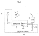
- Fig. 1 is a block diagram showing the structures of the protection circuit according to the first embodiment.
- the protection circuit 10 of the first embodiment is provided, in relation to an amplifier 1, for supplying a voltage signal Vo obtained through amplification of an input voltage signal Vi to a load (for example, speakers) 2.
- a load for example, speakers
- the protection circuit 10 of the first embodiment includes a detection resistor 11, a comparator portion 12, a reference voltage portion 13, and an adder portion 14.
- the detection resistor 11 converts current flowing through the load 2 into voltage (i.e., detection voltage) Vs, to input it into the comparator portion 12.
- the reference voltage portion 13 provides a reference voltage Vb to the comparator portion 12. This reference voltage Vb is selected to a value that can determine on whether current is the over-current or not.
- the comparator portion 12 compares the detection voltage Vs and the reference voltage Vb, and when the detection voltage Vs is larger than the reference voltage Vb, it outputs difference voltage Vs-Vb, or protection voltage Vr obtained by applying a simply increasing function onto that difference voltage, while it outputs 0 when the detection voltage Vs is equal or smaller than the reference voltage Vb.
- the adder portion 14 subtracts the protection voltage Vr or 0, outputted by the comparator portion 12, from the input voltage signal Vi, thereby to supply it to the amplifier 1.
- the adder portion 14 may be provided between the amplifier 1 and the load 2.
- the adder portion 14 subtracts the protection voltage Vr of the comparator portion 12 from the input voltage signal Vi, and inputs a voltage signal Vi-Vr after subtraction to the amplifier 1. This protects the amplifier 1 and the load 2.
- the protection voltage Vr is the difference voltage Vs-Vb between the detection voltage Vs and the reference voltage Vb, or the voltage obtained by applying a simply increasing function onto the difference voltage Vs-Vb.
- the voltage signal Vi-Vr after the subtraction mentioned above when over-current protection functions, has a value being almost constant. In other words, clopping the voltage portion larger than a predetermined level, with respect to such over voltage of the input voltage signal Vi, results in the voltage signal Vi-Vr after the subtraction.
- the first embodiment it is possible to execute the over-current protection through clipping of the input voltage signal, and also to supply the voltage signal to the load 2 continuously.
- the output for generating sounds will not be shut off, as in the conventional protection circuit, and therefore according to the first embodiment, it is possible to continue to provide the output for generating sounds while protecting it from the over-current.
- FIG. 2 is a circuit diagram showing the structures of the protection circuit according to the second embodiment.
- the protection circuit 10A of the second embodiment is also provided, in relation to the amplifier 1, for supplying the voltage signal Vo obtained through amplification of the input voltage signal Vi to the load (for example, speakers) 2.
- the amplifier 1 is shown by a main body of the amplifier AMP, corresponding to a digital amplifier for audio, for example, and a low-pass filter LPF, which is provided at an output stage thereof.
- the protection circuit 10A comprises a first protection circuit for functioning when the input voltage signal Vi is positive, and a second protection circuit for functioning when the input voltage signal Vi is negative.
- each of elements of the first protection circuit is shown by a reference numeral affixed with P at the end thereof, while each of elements of the second protection circuit by a reference numeral affixed with N at the end thereof, except for a detection resistor Rs for over-current.
- the second protection circuit is also similar to the first protection circuit, except for the polarity thereof.
- a resistor R1P for a junction point B of the low-pass filter LPF and the load 2 and a junction point C of the load 2 and the detection resistor Rs, there are connected a resistor R1P, a diode D1P (directing a cathode thereof to the side of resistor R1P), and a resistor R2P, sequentially, in that order from the junction point B.
- a junction point D of an anode of the diode D1P and the resistor R2P is connected to a non-reverse input terminal (i.e., a plus (+) input terminal) of the operational amplifier OPP.
- a reverse input terminal i.e., a minus (-) input terminal
- An output terminal of the operational amplifier OPP is connected to a cathode of the diode P2P, while an anode of this diode D2P is connected the junction point A on a route starting from a signal source to the non-reverse input terminal of the main body of amplifier AMP.
- a resistor R1N Between the junction point B of the low-pass filter LPF and the load 2 and the junction point C of the load 2 and the detection resistor Rs, there are connected a resistor R1N, a diode D1N (directing a cathode thereof to the side of resistor R1N), and a resistor R2N, sequentially, in that order from the junction point B.
- a junction point E of a cathode of the diode D1N and the resistor R2N is connected to a non-reverse input terminal (i.e., a plus (+) input terminal) of an operational amplifier OPN.
- a reverse input terminal i. e. , a minus (-) input terminal
- Vb To a reverse input terminal (i. e. , a minus (-) input terminal) of the operational amplifier OPN is connected a reference positive voltage Vb.
- An output terminal of the operational amplifier OPN is connected to of an anode the diode D2N, while a cathode of this diode D2N is also connected the junction point A on a route starting from the signal source to the non-reverse input terminal of the main body of amplifier AMP.
- the input voltage signal Vi from the signal-generating source shown in Fig. 3A is amplified by means of the amplifier 1, and it comes to the output voltage signal Vo to the load 2, as shown in Fig. 3B. Applying this output voltage signal Vo thereon, current flowing through the load 2 is converted into the detection voltage signal Vs, as shown in Fig. 3C, by means of the detection resistor Rs.
- This second embodiment is for a case where the current flowing through the load 2 is oppositely phased in a relationship to the output voltage signal Vo, and for that reason, the detection voltage signal Vs is also oppositely phased in the relationship to the output voltage signal Vo.
- the junction point B is connected to the non-reverse input terminal of the operational amplifier OPP through the resistor R1P and the diode D1P, and the junction point C is connected to the non-reverse input terminal of the operational amplifier OPP through the resistor R2, an addition value (Vo+Vs) of the output voltage signal Vo and the detection voltage signal Vs are inputted to the non-reverse input terminal of the operational amplifier OPP.
- the detection voltage signal Vs is oppositely phased in the relationship to the output voltage signal Vo and they are in such relationship, i.e.,
- +Vb takes a negative value, as shown in Fig. 3(EP).
- +Vb also takes a positive value.
- Fig. 3(EP) shows the output from the operational amplifier OPP,
- Fig. 3F shows the input voltage signal Vi after clipping the positive and negative large values of such input voltage signal Vi causing the over-current. Since this clipped input voltage signal Vi is inputted into the amplifier 1, the output voltage signal Vo from the amplifier 1 also comes to be clipped on the large values thereof, as shown in Fig. 3G, and the current flowing into the load 2 also comes to be clipped on the large values thereof, as shown in Fig. 3H. Thus, the over-current is suppressed, and the load 2 is protected from the over-current and/or the voltage Vo applied thereon.
- Fig. 4 shows the signal waveforms of the output voltage waveforms
- the roundness is changed on the output voltage waveforms
- OPP and OPN
- Fig. 5 shows foldback current limiting characteristics between the voltage Vo applied onto the load and the load current Io, when the load is short-circuited. Making such foldback current limiting characteristics can finally suppress the short-circuited current down to I2, thereby reducing the load applied upon the amplifier when the load is short-circuited.
- the second embodiment it is possible to reduce the load of the amplifier provided at a front stage of the load, while suppressing the short-circuiting current to be small when the load is short-circuited.
- the reference voltage is inputted to the reverse input terminals of the operational amplifiers OPP and OPN.
- reference voltages opposite in the polarity i.e., positive and negative
- reference voltages opposite in the polarity i.e., positive and negative
- the input voltage signal Vi to the amplifier 1 and the output voltage signal Vo from the amplifier 1 are same in the phase.
- the present invention can be applied to the case where the input voltage signal Vi to the amplifier 1 and the output voltage signal Vo from the amplifier 1 are oppositely phased, as shown in Figs. 7A and 7B.
- Fig. 8 shows an example of the structures of the protection circuit in case of opposite phase thereof, as mentioned above, wherein the input terminals for the signals to the operational amplifiers OPP and OPN are reversed to those of the second embodiment, and also the reference voltages are reversed the polarity thereof.
- protection circuits intended to be applied to a system which supplies the audio signal (i.e., the voltage signal) from the audio amplifier to the speakers; however, the protection circuit according to the present invention may be also applied where the power source from an electric power source circuit is supplied to the load.
- the protection circuit according to the present invention may be applied to the protection circuit, in a case where the signal generation source in Fig. 2 is the electric power source circuit and the amplifier 1 is omitted to supply the electric power to the load 2.
Landscapes
- Engineering & Computer Science (AREA)
- Power Engineering (AREA)
- Amplifiers (AREA)
- Emergency Protection Circuit Devices (AREA)
- Power Conversion In General (AREA)
- Tone Control, Compression And Expansion, Limiting Amplitude (AREA)
Applications Claiming Priority (1)
| Application Number | Priority Date | Filing Date | Title |
|---|---|---|---|
| JP2005259761A JP2007074431A (ja) | 2005-09-07 | 2005-09-07 | 保護回路 |
Publications (1)
| Publication Number | Publication Date |
|---|---|
| EP1763130A1 true EP1763130A1 (de) | 2007-03-14 |
Family
ID=37649312
Family Applications (1)
| Application Number | Title | Priority Date | Filing Date |
|---|---|---|---|
| EP06018469A Withdrawn EP1763130A1 (de) | 2005-09-07 | 2006-09-04 | Schutzschaltung |
Country Status (3)
| Country | Link |
|---|---|
| US (1) | US20070053128A1 (de) |
| EP (1) | EP1763130A1 (de) |
| JP (1) | JP2007074431A (de) |
Families Citing this family (7)
| Publication number | Priority date | Publication date | Assignee | Title |
|---|---|---|---|---|
| JP4960764B2 (ja) * | 2007-05-21 | 2012-06-27 | ティーオーエー株式会社 | 増幅器 |
| JP4492640B2 (ja) * | 2007-05-30 | 2010-06-30 | ヤマハ株式会社 | 増幅器 |
| KR20100098654A (ko) * | 2007-12-31 | 2010-09-08 | 인터실 아메리카스 인코포레이티드 | 개선된 과전류 클리핑 시스템 및 방법 |
| DE102008043352A1 (de) * | 2008-10-31 | 2010-05-06 | Micro Systems Engineering Gmbh | Keramisches Substratmaterial, Verfahren zur Herstellung und Verwendung desselben sowie Antenne oder Antennenarray |
| US9124461B2 (en) * | 2011-07-18 | 2015-09-01 | Marvell Israel (M.I.S.L) Ltd. | Method and apparatus for reducing jitter |
| CN108574462B (zh) * | 2018-01-31 | 2021-03-26 | 中兴通讯股份有限公司 | 保护电路、电路保护方法 |
| US12334878B2 (en) | 2021-11-22 | 2025-06-17 | Samsung Electronics Co., Ltd. | Electronic device and method including power amplifier module having protection circuit |
Citations (7)
| Publication number | Priority date | Publication date | Assignee | Title |
|---|---|---|---|---|
| US3681659A (en) * | 1970-03-26 | 1972-08-01 | Sony Corp | Amplifier protective circuit |
| US3990020A (en) * | 1975-06-26 | 1976-11-02 | Hughes Aircraft Company | DC linear power amplifier |
| US3992678A (en) * | 1972-07-27 | 1976-11-16 | Sony Corporation | Protective circuit for transistor amplifier |
| US4180768A (en) * | 1978-07-20 | 1979-12-25 | Tele/Resources, Incorporated | Energy limiting foldback circuit for power supply |
| US4509101A (en) * | 1982-08-24 | 1985-04-02 | Nippon Gakki Seizo Kabushiki Kaisha | Protection circuit for switching power amplifier |
| JPH09270652A (ja) | 1996-03-29 | 1997-10-14 | Sanyo Electric Co Ltd | 増幅回路 |
| US20040135635A1 (en) * | 2002-12-27 | 2004-07-15 | Yamaha Corporation | Amplifier circuitry |
-
2005
- 2005-09-07 JP JP2005259761A patent/JP2007074431A/ja active Pending
-
2006
- 2006-08-31 US US11/513,056 patent/US20070053128A1/en not_active Abandoned
- 2006-09-04 EP EP06018469A patent/EP1763130A1/de not_active Withdrawn
Patent Citations (7)
| Publication number | Priority date | Publication date | Assignee | Title |
|---|---|---|---|---|
| US3681659A (en) * | 1970-03-26 | 1972-08-01 | Sony Corp | Amplifier protective circuit |
| US3992678A (en) * | 1972-07-27 | 1976-11-16 | Sony Corporation | Protective circuit for transistor amplifier |
| US3990020A (en) * | 1975-06-26 | 1976-11-02 | Hughes Aircraft Company | DC linear power amplifier |
| US4180768A (en) * | 1978-07-20 | 1979-12-25 | Tele/Resources, Incorporated | Energy limiting foldback circuit for power supply |
| US4509101A (en) * | 1982-08-24 | 1985-04-02 | Nippon Gakki Seizo Kabushiki Kaisha | Protection circuit for switching power amplifier |
| JPH09270652A (ja) | 1996-03-29 | 1997-10-14 | Sanyo Electric Co Ltd | 増幅回路 |
| US20040135635A1 (en) * | 2002-12-27 | 2004-07-15 | Yamaha Corporation | Amplifier circuitry |
Also Published As
| Publication number | Publication date |
|---|---|
| JP2007074431A (ja) | 2007-03-22 |
| US20070053128A1 (en) | 2007-03-08 |
Similar Documents
| Publication | Publication Date | Title |
|---|---|---|
| EP1887830A2 (de) | Schutzschaltung und Laststromerkennungsschaltung | |
| JP5228840B2 (ja) | 増幅器 | |
| EP2244378A2 (de) | Verstärkerschaltung, Wechselstromverstärkerschaltung und Verfahren zum Einstellen der Eingangsvorspannung | |
| EP1763130A1 (de) | Schutzschaltung | |
| JP4960764B2 (ja) | 増幅器 | |
| JP2008244623A (ja) | 半導体集積回路 | |
| JP2008009968A (ja) | 電圧発生装置、電流発生装置および試験装置 | |
| US10312872B2 (en) | Managing a shoot-through condition in a component containing a push-pull output stage | |
| US9319041B1 (en) | Squelch detector | |
| US20190089242A1 (en) | Power supply device and method of controlling power supply device | |
| JPH02250564A (ja) | クランプ装置と自動利得制御装置 | |
| EP0921635B1 (de) | Leistungsverstärker | |
| JP4083551B2 (ja) | 前置増幅器 | |
| JP2001203536A (ja) | 検波回路及び送信装置 | |
| US20220224293A1 (en) | Class-d amplifier, a method of controlling a gain of an input audio signal in a class-d amplifier | |
| JP4261316B2 (ja) | オーディオ回路 | |
| JP3665841B2 (ja) | 電力増幅器 | |
| US7498798B2 (en) | Current-to-voltage detection circuit | |
| KR101877381B1 (ko) | 병렬 구조 직류-직류 컨버터 제어 시스템 및 방법 | |
| JP7279903B1 (ja) | 電源システム、電源システムが実行する処理方法およびプログラム | |
| US20010050593A1 (en) | Circuit for detecting distortion in an amplifier, in particular an audio amplifier | |
| US20250167740A1 (en) | Class d amplifier capable of anti-clipping | |
| JPH066308A (ja) | 光受信用agc回路 | |
| JP2617616B2 (ja) | パイロット信号除去回路 | |
| US20060055462A1 (en) | Amplifier circuit and gain control method |
Legal Events
| Date | Code | Title | Description |
|---|---|---|---|
| PUAI | Public reference made under article 153(3) epc to a published international application that has entered the european phase |
Free format text: ORIGINAL CODE: 0009012 |
|
| AK | Designated contracting states |
Kind code of ref document: A1 Designated state(s): AT BE BG CH CY CZ DE DK EE ES FI FR GB GR HU IE IS IT LI LT LU LV MC NL PL PT RO SE SI SK TR |
|
| AX | Request for extension of the european patent |
Extension state: AL BA HR MK YU |
|
| RIN1 | Information on inventor provided before grant (corrected) |
Inventor name: YOKOYAMA, KENJI Inventor name: OGAWA, HIROSHI Inventor name: SAWAI, KEISUKE Inventor name: MIZUSHIMA, TAKAAKI |
|
| 17P | Request for examination filed |
Effective date: 20070905 |
|
| 17Q | First examination report despatched |
Effective date: 20071005 |
|
| AKX | Designation fees paid |
Designated state(s): DE FR GB IT NL |
|
| STAA | Information on the status of an ep patent application or granted ep patent |
Free format text: STATUS: THE APPLICATION IS DEEMED TO BE WITHDRAWN |
|
| 18D | Application deemed to be withdrawn |
Effective date: 20080416 |