EP1763228A2 - Méthode et circuit de réduction de scintillement et dispositif de prise de vue - Google Patents
Méthode et circuit de réduction de scintillement et dispositif de prise de vue Download PDFInfo
- Publication number
- EP1763228A2 EP1763228A2 EP06254612A EP06254612A EP1763228A2 EP 1763228 A2 EP1763228 A2 EP 1763228A2 EP 06254612 A EP06254612 A EP 06254612A EP 06254612 A EP06254612 A EP 06254612A EP 1763228 A2 EP1763228 A2 EP 1763228A2
- Authority
- EP
- European Patent Office
- Prior art keywords
- flicker
- component
- computationally
- fluorescent lamp
- lighting
- Prior art date
- Legal status (The legal status is an assumption and is not a legal conclusion. Google has not performed a legal analysis and makes no representation as to the accuracy of the status listed.)
- Granted
Links
Images


Classifications
-
- H—ELECTRICITY
- H04—ELECTRIC COMMUNICATION TECHNIQUE
- H04N—PICTORIAL COMMUNICATION, e.g. TELEVISION
- H04N23/00—Cameras or camera modules comprising electronic image sensors; Control thereof
- H04N23/70—Circuitry for compensating brightness variation in the scene
- H04N23/745—Detection of flicker frequency or suppression of flicker wherein the flicker is caused by illumination, e.g. due to fluorescent tube illumination or pulsed LED illumination
-
- H—ELECTRICITY
- H04—ELECTRIC COMMUNICATION TECHNIQUE
- H04N—PICTORIAL COMMUNICATION, e.g. TELEVISION
- H04N23/00—Cameras or camera modules comprising electronic image sensors; Control thereof
- H04N23/70—Circuitry for compensating brightness variation in the scene
-
- H—ELECTRICITY
- H04—ELECTRIC COMMUNICATION TECHNIQUE
- H04N—PICTORIAL COMMUNICATION, e.g. TELEVISION
- H04N25/00—Circuitry of solid-state image sensors [SSIS]; Control thereof
- H04N25/70—SSIS architectures; Circuits associated therewith
- H04N25/76—Addressed sensors, e.g. MOS or CMOS sensors
Definitions
- the present invention contains subject matter related to Japanese Patent Application JP 2005-261095 filed in the Japanese Patent Office on September 8, 2005, the entire contents of which being incorporated herein by reference.
- the present invention relates to a flicker-reduction method and a flicker-reduction circuit to be used for an image pickup apparatus such as a video camera or a digital still camera including an XY address scanning type imaging element (imager, image sensor), which may typically be a CMOS (complementary metal oxide semiconductor) imaging element, under the lighting of a fluorescent lamp and also to an image pickup apparatus adapted to use such a method and such a circuit.
- an image pickup apparatus such as a video camera or a digital still camera including an XY address scanning type imaging element (imager, image sensor), which may typically be a CMOS (complementary metal oxide semiconductor) imaging element, under the lighting of a fluorescent lamp and also to an image pickup apparatus adapted to use such a method and such a circuit.
- imager image sensor
- CMOS complementary metal oxide semiconductor
- the timing of exposure relative to the luminance change of the fluorescent lamp returns to the original one in every three fields and therefore the change of lightness is cyclic and repetitive with a period of three fields.
- the luminance ratio of each field (how flickering appears) changes with the exposure period but the period of flicker does not change.
- the change of lightness in every three frames is repeated with progressive type cameras such as digital cameras when the vertical synchronizing frequency is 30 Hz.
- CMOS imaging element In the case of an XY address scanning type imaging element, which may typically be a CMOS imaging element, the timing of exposure of each pixel is sequentially shifted from that of the preceding pixel in the horizontal direction by a clock (pixel clock) period and hence the timings of exposure of all the pixels differ from each other so that flicker arises in each frame and recognized as a pattern of black strips in the image. In other words, there arises a seriously degraded image.
- a flicker-reduction method for reducing a flicker component of a fluorescent lamp contained in a video signal obtained by shooting a subject by means of an XY address scanning type imaging element under a lighting of a fluorescent lamp, the method including: an integration step of integrating the input video signal obtained by shooting the subject over a time period greater than a horizontal period; a normalization step of normalizing an integral value obtained in the integration step or the difference value between integral values of adjacent fields or frames: an extraction step of extracting the spectrum of the integral value or the difference value normalized in the normalization step; an estimation step of estimating the flicker component from the spectrum extracted in the extraction step; a subtraction step of acquiring the current integral value obtained by integrating the input video signal over a time period greater than a horizontal period and the integral value of a field preceding the current field by several fields and determining the difference of the integral values; a computation step of computing the probability of being under the lighting of a fluorescent lamp from the difference of the integral values determined in the
- a flicker-reduction circuit for reducing a flicker component of a fluorescent lamp contained in a video signal obtained by shooting a subject by means of an XY address scanning type imaging element under a lighting of a fluorescent lamp
- the circuit including: an integration means for integrating the input video signal obtained by shooting the subject over a time period greater than a horizontal period; a normalization means for normalizing an integral value obtained by the integration means or the difference value between integral values of adjacent fields or frames; an extraction means for extracting the spectrum of the integral value or the difference value normalized by the normalization means; an estimation means for estimating the flicker component from the spectrum extracted by the extraction means; a subtraction means for acquiring the current integral value obtained by integrating the input video signal over a time period greater than a horizontal period and the integral value of a field preceding the current field by several fields and determining the difference of the integral values; a computation means for computing the probability of being under the lighting of a fluorescent lamp from the difference of the integral values determined by
- an image pickup apparatus having a flicker-reduction circuit for reducing a flicker component of a fluorescent lamp contained in a video signal obtained by shooting a subject by means of an XY address scanning type imaging element under a lighting of a fluorescent lamp
- the circuit including: an integration means for integrating the input video signal obtained by shooting the subject over a time period greater than a horizontal period; a normalization means for normalizing an integral value obtained by the integration means or the difference value between integral values of adjacent fields or frames; an extraction means for extracting the spectrum of the integral value or the difference value normalized by the normalization means; an estimation means for estimating the flicker component from the spectrum extracted by the extraction means; a subtraction means for acquiring the current integral value obtained by integrating the input video signal over a time period greater than a horizontal period and the integral value of a field preceding the current field by several fields and determining the difference of the integral values; a computation means for computing the probability of being under the lighting of a fluorescent lamp from the difference of
- CMOS elements complementary metal-oxide-semiconductor
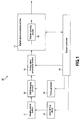
- the present invention is applicable to an image pickup apparatus having a configuration shown in FIG. 1.
- the image pickup apparatus 10 is a video camera realized by using an XY address scanning type imaging element, which is a CMOS imaging element 12.
- the image pickup apparatus 10 includes an imaging optical system 11, a CMOS imaging element 12, an analog signal processing section 13, a system controller 14, a lens driving driver 15, a timing generator 16 and a digital signal processing section 17.
- this image pickup apparatus 10 With this image pickup apparatus 10, light from a subject enters the CMOS imaging element 12 by way of an imaging optical system 11 and is subjected to photoelectric conversion in the CMOS imaging element 12 so that analog video signals are obtained from the CMOS imaging element 12.
- the CMOS imaging element 12 is formed by arranging a plurality of pixels having photodiodes (photo gates), transfer gates (shutter transistors), switching transistors (address transistors), amplifier transistors and reset transistors (reset gates) two-dimensionally on a CMOS substrate along with a vertical scanning circuit, a horizontal scanning circuit and a video signal output circuit.
- the CMOS imaging element 12 may be of the primary color system or of the complementary color system and the analog video signals obtained from the CMOS imaging element 12 may be primary color signals of RGB or color signals of the complementary color system.
- the analog video signals from the CMOS imaging element 12 are subjected to a sample hold process for each color by analog signal processing section 13 that is realized as an IC (integrated circuit) and controlled for the gain by AGC (automatic gain control) before being converted into digital signals by A/D conversion.
- analog signal processing section 13 that is realized as an IC (integrated circuit) and controlled for the gain by AGC (automatic gain control) before being converted into digital signals by A/D conversion.
- the digital video signals from the analog signal processing section 13 are processed by digital signal processing section 17 that is realized as an IC and the flicker component of each signal is reduced by flicker reducing section 18 in the digital signal processing section 17 before they are ultimately converted into luminance signals Y and color difference signals R-Y, B-Y and output from the digital signal processing section 17.
- the system controller 14 is typically realized as a microcomputer so as to control the components of the camera.
- a lens drive control signal is supplied from the system controller 14 to lens driving driver 15 that is realized as IC and the lenses of the imaging optical system 11 are driven by the lens driving driver 15.
- timing control signal is supplied from the system controller 14 to the timing generator 16 and various timing signals are supplied from the timing generator 16 to the CMOS imaging element 12 to drive the CMOS imaging element 12.
- the detection signal of each signal component is taken into the system controller 14 from the digital signal processing section 17 so that color signals of different colors are controlled for gain by the analog signal processing section 13 according to the AGC signal from the system controller 14 as described above and the signal processing operation of the digital signal processing section 17 is also controlled by the system controller 14.
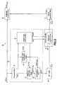
- the flicker reducing section 18 arranged in the above-described digital signal processing section 17 includes a normalization process block 20 and an arithmetic operation block 30, to which digital video signals are supplied from the above-described analog signal processing section 13, as well as a DFT block 40 connected the normalization process block 20 and a flicker generation block 41 connected to the arithmetic operation block 30.
- the normalization process block 20 by turn includes an integration block 21, to which input video signals In'(x, y), or digital video signals, are supplied from the above-described analog signal processing section 13, an integral value retaining block 22 connected to the integration block 21, an average value computing block 23, a difference computing block 24, and a normalization block 25.
- the flicker component is generally proportional to the signal intensity of the subject.
- In' (x, y) is the sum of the signal component that does not contain the flicker component and the flicker component that is proportional to the signal component as expressed by the formula (1) shown below.
- In ⁇ x ⁇ y 1 + ⁇ n y ⁇ ln x ⁇ y
- In (x, y) is the signal component and ⁇ n (y) ⁇ In (x, y) is the flicker component, where ⁇ n (y) is the flicker coefficient. Since a horizontal period is very short relative to the light emitting period of the fluorescent lamp, it is possible to assume that the flicker coefficient is constant for the same line in the same field. Therefore, the flicker coefficient is expressed by ⁇ n (y).
- ⁇ ⁇ ⁇ m , n - m ⁇ ⁇ 0 ⁇ 2 ⁇ ⁇
- the input video signal In'(x, y) is integrated over a line in the horizontal direction of the image plane to determine the integral value Fn (y) as expressed by formula (4) shown below in order, which reduces the influence of the image pattern when detecting flicker.
- an (y) is the integral value over a line of the signal component In(x, y) that is expressed by formula (5) shown below.
- ⁇ n y ⁇ X ln x ⁇ y
- the computationally determined integral value Fn (y) is stored and retained in integral value retaining block 22 for the purpose of flicker detection in the subsequent fields.
- the integral value retaining block 22 is so designed as to be able to retain the integral values of at least K fields.
- K is the number of fields necessary for canceling the flicker component that is obtained from the vertical synchronizing frequency fv and the frequency of the fluorescent lamp by means of formula (6) shown below.
- GCD is a function for determining the greatest common divisor.
- K f V GCD 2 ⁇ f L , f V
- the integral value ⁇ n (y) of the signal component In (x, y) is a constant value and hence it is easy to extract the flicker component ⁇ n (y) ⁇ ⁇ n (y) from the integral value Fn (y) of the input video signal In' (x, y).
- a subject generally contains m ⁇ ⁇ o component in ⁇ n (y) and hence it is not possible to isolate the luminance component and the color component of the flicker component from the luminance component and the color component of the signal component of the subject itself. In short, it is not possible to purely extract only the flicker component. Additionally, since the flicker component of the second term is very small relative to the signal component of the first term in the formula (4), the flicker component is substantially buried in the signal component.
- the flicker reducing section 18 uses the integral value of continuous K fields in order to remove the influence of ⁇ n (y) from the integral value Fn(y).
- the integral value Fn (y) of a line when computationally determining the integral value Fn (y) of a line, the integral value Fn - (K-1) (y) of the same line in the (K - 1) preceding field and the integral value Fn_1 (y) of the same line in the immediately preceding field are read out from an integral value retaining block 22 and the average vale AVE [Fn (y)] ofK integral values Fn (y), ..., Fn - (K - 1) (y) is computationally determined.
- the flicker reducing section 18 provided for a situation where the movement of the subject is large retains the integral values of not less than three fields in the integral value retaining block 22 and computationally determines the average value of the integral values of not less than (K + 1) fields including the integral value Fn (y) of the current field.
- the flicker reducing section 18 provided for a situation where the movement of the subject is large retains the integral values of not less than three fields in the integral value retaining block 22 and computationally determines the average value of the integral values of not less than (K + 1) fields including the integral value Fn (y) of the current field.
- the normalization block 25 normalizes the difference value Fn (y) - Fn_1 (y) from the difference computing block 24 as it divides the difference value by the average value AVE [Fn (y)] from the average value computing block 23 to computationally determine the normalized difference value gn (y).
- the normalized difference value gn (y) is developed into formula (10) shown below by means of the above formula (7) and formula (9) shown below and the addition/multiplication formula of trigonometric function and expressed by formula (11) below from the relationship of the above formula (3).
- the level of the luminance change and that of the color change due to flickering can vary depending on an area in the image.
- the level of the luminance change and that of the color change can be equalized over all the areas of the image as a result of the above-described normalization.
- DFT block 40 performs a discrete Fourier transform of the data that corresponds to the wavelength (for line L) of the flicker in the normalized difference value gn (y) obtained from the normalization block 25.
- W in the formula (16) is expressed by formula (17) shown below.
- W exp - j ⁇ 2 ⁇ ⁇ L
- the data length of the DFT operation is made equal to the wavelength of the flicker because, by doing so, it is made possible to directly obtain a group of discrete spectra of integer times of ⁇ o.
- FFT fast Fourier transform
- the DFT block 40 firstly extracts spectra with a DFT operation defined by the formula (16) and subsequently the amplitude ⁇ m and the initial phase ⁇ mn of the flicker component of each degree are estimated by means of operations using the formulas (21) and (22).
- the flicker generation block 41 computationally determines the flicker coefficient ⁇ n (y) expressed by the above-described formula (2) from the estimated values of ⁇ m and ⁇ mn obtained from the DFT block 40.
- arithmetic operation block 30 adds one to the flicker coefficient ⁇ n (y) obtained from the flicker generation block 41 and divides the input video signal In' (x, y) by the sum [1 + ⁇ n (y)].
- the system controller 14 of the image pickup apparatus 10 receives the amplitude ⁇ m and the initial phase ⁇ mn of the flicker component from the DFT block 40 of the above-described flicker reducing section 18 as inputs and is provided with a parameter control section 14*, to which the integral value Y(n) and the integral value Y(n - k) of the flicker detecting area of the K preceding field from the integral value retaining block 22 are supplied.
- the parameter control section 14* may typically be a parameter control section 14A having a configuration as shown in FIG. 4.
- the parameter control section 14A includes an amplitude gain computing section 50 and a multiplier 55.
- the parameter control section 14A receives as inputs the amplitude ⁇ m and the initial phase ⁇ mn of the flicker component of each degree determined by the DFT block 40.
- the amplitude gain computing section 50 is adapted to output the suppressed gain of the amplitude ⁇ m of the flicker component from both the total integral value Y(n) of the current flicker detecting area and the total integral value Y(n - k) of the flicker detecting area of the K preceding field.
- the amplitude gain computing section 50 includes a subtracter 51, to which the integral value Y (n) of the current flicker detecting area and the integral value Y(n - k) of the flicker detecting area of the K preceding field are supplied from the integral value retaining block 22, an absolute value (ABS) circuit 52 connected to the subtracter 51, a low pass filter (LPF) 53 connected to the ABS circuit 52, and a gain computing section 54 connected to the LPF 53.
- ABS absolute value
- LPF low pass filter
- the subtracter 51 computationally determines the difference integral value ⁇ Y(n) of the current integral value Y(n) and the integral value Y(n - K) of the K preceding field.
- the ABS circuit 52 turns the output value of the subtracter 51 into the corresponding absolute value.
- the output value of the subtracter 51 is small, it is possible to presume that there is no moving subject and the amplitude ⁇ m is regarded to be highly reliable. If, on the other hand, the output value of the subtracter 51 is large, the amplitude ⁇ m is regarded to be lowly reliable because it is possible to presume that there is a moving subject.
- the LPF 53 is a filter for reducing any excessive fluctuations of the difference integral value
- the LPF is preferably arranged with a time constant that provides a time period good for stably determining if the scene to be shot is under the lighting of a fluorescent lamp or under the lighting of non-fluorescent lamp and prevents the LPF from reacting to external turbulences too sensitively.
- the gain computing section 54 outputs a value between 0 and 1 according to the output value of the LPF 53 as shown in FIG. 5. More specifically, the gain computing section 54 outputs 0 when the output value of the LPF 53 is greater than a threshold value thrB, whereas it outputs 1 when the output value of the LPF 53 is smaller than a threshold value thrA but it outputs a linearly interpolated value when the output value of the LPF 53 is between the threshold value thrA and the threshold value thrB. In short, it outputs 1 when the reliability of the output of the LPF 53 is high but 0 when the reliability is low.
- the multiplier 55 multiplies the amplitude ⁇ m of the flicker component of each degree by the output value of the gain computing section 54.
- the gain computing process is executed for each degree of DFT.
- the first degree of DFT is the main component.
- the gain is computationally determined constantly for higher degrees because any spectrum other than that of a fluorescent lamp is shifted far from the phase component of a fluorescent lamp and the gain is suppressed consequently.
- FIG. 6 is a flowchart of the sequence of control operation of the parameter control section 14A.
- Step S 10 the difference between the current integral value Y(n) and the integral value Y(n - K) of the K preceding field is set to difference integral value ⁇ Y(n).
- Step S 11 the absolute value of the different integral value ⁇ Y(n) is set to ⁇ Y ABS (n).
- Step S12 the value obtained by applying an LPF process to ⁇ Y ABS (n) is set to ⁇ Y LPF_ABS (n).
- Step S 13 the suppressed gain is computationally determined by means of the function shown in FIG. 5 from ⁇ Y LPF_ABS (n).
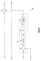
- the present invention can be applied to an image pickup apparatus 100 having a configuration as shown in FIG. 7.
- the image pickup apparatus 100 is a video camera realized by using an XY address scanning type imaging element, which is a CMOS imaging element 112.
- the image pickup apparatus 100 includes an imaging optical system 111, a CMOS imaging element 112, an analog signal processing section 113, a system controller 114, a lens driving driver 115, a timing generator 116, a digital signal processing section 117, and a luminance detecting section 119.
- this image pickup apparatus 100 With this image pickup apparatus 100, light from a subject enters the CMOS imaging element 112 by way of an imaging optical system 111 and is subjected to photoelectric conversion in the CMOS imaging element 112 so that analog video signals are obtained from the CMOS imaging element 112.
- the CMOS imaging element 112 is formed by arranging a plurality of pixels having photodiodes (photo gates), transfer gates (shutter transistors), switching transistors (address transistors), amplifier transistors and reset transistors (reset gates) two-dimensionally on a CMOS substrate along with a vertical scanning circuit, a horizontal scanning circuit, and a video signal output circuit.
- the CMOS imaging element 112 may be of the primary color system or of the complementary color system and the analog video signals obtained from the CMOS imaging element 112 may be primary color signals of RGB or color signals of the complementary color system.
- analog video signals from the CMOS imaging element 112 are subjected to a sample hold process for each color by analog signal processing section 113 that is realized as an IC (integrated circuit) and controlled for the gain by AGC (automatic gain control) before being converted into digital signals by A/D conversion.
- analog signal processing section 113 that is realized as an IC (integrated circuit) and controlled for the gain by AGC (automatic gain control) before being converted into digital signals by A/D conversion.
- the digital video signals from the analog signal processing section 113 are processed by digital signal processing section 117 that is realized as an IC and the flicker component of each signal is reduced by flicker reducing section 118 in the digital signal processing section 117 before they are ultimately converted into luminance signals Y and color difference signals R-Y, B-Y and output from the digital signal processing section 117.
- the digital video signals from the analog signal processing section 113 are supplied to the luminance detecting section 119, which luminance detecting section 119 outputs the current luminance level Y(n) and the luminance level of the K preceding field Y(n - K) to the system controller 114.
- the system controller 114 is typically realized as a microcomputer so as to control the components of the camera.
- a lens drive control signal is supplied from the system controller 114 to lens driving driver 115 that is realized as IC and the lenses of the imaging optical system 111 are driven by the lens driving driver 115.
- timing control signal is supplied from the system controller 114 to timing generator 116 and various timing signals are supplied from the timing generator 116 to the CMOS imaging element 112 to drive the CMOS imaging element 112.
- the detection signal of each signal component is taken into the system controller 114 from the digital signal processing section 117 so that color signals of different colors are controlled for gain by the analog signal processing section 113 according to the AGC signal from the system controller 114 as described above and the signal processing operation of the digital signal processing section 120 is also controlled by the system controller 114.
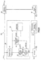
- the flicker reducing section 18 arranged in the above-described digital signal processing section 117 includes a normalization process block 120 and an arithmetic operation block 130, to which digital video signals are supplied from the above-described analog signal processing section 113, as well as a DFT block 140 connected to the normalization process block 120 and a flicker generation block 141 connected to the arithmetic operation block 130.
- the normalization process block 120 by turn includes an integration block 121, to which input video signals In'(x, y), or digital video signals, are supplied from the above-described analog signal processing section 113, an integral value retaining block 122 connected to the integration block 121, an average value computing block 123, a difference computing block 124, and a normalization block 125.
- the input video signal In'(x, y) is integrated over a line in the horizontal direction of the image plane to determine the integral value Fn (y) by the integration block 121 as expressed by the above-described formula (4) shown below in order to reduce the influence of the image when detecting flicker.
- the integral value Fn (y) that is computationally determined by the integration block 121 is stored and retained in integral value retaining block 122 for the purpose of flicker detection in the subsequent fields.
- the integral value retaining block 122 is so designed as to be able to retain the integral values of at least K fields.
- K is the number of fields necessary for canceling the flicker component that is obtained from the vertical synchronizing frequency fv and the frequency of the fluorescent lamp f1 by means of the above-described formula (6).
- GCD is a function for determining the greatest common divisor.
- the integral value an (y) of the signal component In (x, y) is a constant value and hence it is easy to extract the flicker component ⁇ n (y) * ⁇ n (y) from the integral value Fn (y) of the input video signal In' (x, y).
- a subject generally contains m * ⁇ o component in ⁇ n (y) and hence it is not possible to isolate the luminance component and the color component of the flicker component from the luminance component and the color component of the signal component of the subject itself. In short, it is not possible to purely extract only the flicker component. Additionally, since the flicker component of the second term is very small relative to the signal component of the first term in the formula (4), the flicker component is substantially buried in the signal component.
- the flicker reducing section 18 uses the integral value of continuous K fields in order to remove the influence of ⁇ n (y) from the integral value Fn (y).
- the integral value Fn - (K - 1) (y) of the same line in the (K - 1) preceding field and the integral value Fn_1 (y) of the same line in the immediately preceding field are read out from an integral value retaining block 122 and the average vale AVE [Fn (y)] of K integral values Fn (y), ..., Fn - (K - 1) (y) is computationally determined from the average value computing block 123.
- the subject can be regarded substantially same in the period of the K consecutive fields, it is possible to regard the value of ⁇ n (y) same for the K consecutive fields. If the movement of the subject is sufficiently small in the K fields, the above assumption does not practically give rise to any problem. Additionally, when computing the average value of the integral values of K consecutive fields, the signals where the phase of the flicker component is sequentially shifted by - ⁇ 0 ⁇ m ⁇ 2 ⁇ are added as seen from the relationship of the above-described formula (3). Thus, consequently the flicker components are cancelled. Therefore, the average value AVE [Fn (y)] is expressed by the above-described formula (7).
- the flicker reducing section 18 provided for a situation where the movement of the subject is large retains the integral values of not less than three fields in the integral value retaining block 122 and computationally determines the average value of the integral values of not less than (K + 1) fields including the integral value Fn (y) of the current field.
- the flicker reducing section 18 provided for a situation where the movement of the subject is large retains the integral values of not less than three fields in the integral value retaining block 122 and computationally determines the average value of the integral values of not less than (K + 1) fields including the integral value Fn (y) of the current field.
- the normalization block 125 normalizes the difference value Fn (y) - Fn_1 (y) from the difference computing block 124 as it divides the difference value by the average value AVE [Fn (y)] from the average value computing block 123 to computationally determine the normalized difference value gn (y).
- the normalized difference value gn (y) is expressed by the above-described formula (11).
- the level of the luminance change and that of the color change due to flickering can vary depending on the area in the image.
- the level of the luminance change and that of the color change can be equalized over all the areas of the image as a result of the above-described normalization.
- DFT block 140 performs a discrete Fourier transform of the data that corresponds to the wavelength (for line L) of the flicker in the normalized difference value gn (y) obtained from the normalization block 125.
- the DFT operation is DFT [gn (y)] and the result of the DFT of degree m is Gn (m), the DFT operation is expressed by the above-described formula (16).
- the data length of the DFT operation is made equal to the wavelength of the flicker (for line L) because, by doing so, it is made possible to directly obtain a group of discrete spectra of integer times of ⁇ o.
- FFT fast Fourier transform
- the DFT block 40 firstly extracts spectra with a DFT operation defined by the above-described formula (16) and subsequently the amplitude ⁇ m and the initial phase ⁇ mn of the flicker component of each degree are estimated by means of operations using the above-described formulas (21) and (22).
- the flicker generation block 141 computationally determines the flicker coefficient ⁇ n (y) expressed by the above-described formula (2) from the estimated values of ⁇ m and ⁇ mn obtained from the DFT block 140.
- the signal component In (x, y) that does not contain any flicker component is expressed by the above-described formula (22).
- arithmetic operation block 130 adds one to the flicker coefficient ⁇ n (y) obtained from the flicker generation block 141 and divides the input video signal In' (x, y) by the sum [1 + ⁇ n (y)].
- the flicker component that is contained in the input video signal In' (x, y) is substantially completely eliminated and a signal component In (x, y) that practically does not contain any flicker component is obtained as output video signal (RGB primary color signal or luminance signal with a reduced flicker) from the arithmetic operation block 130.
- the system controller 114 of the image pickup apparatus 110 receives the amplitude ⁇ m and the initial phase ⁇ mn of the flicker component from the DFT block 140 of the above-described flicker reducing section 118 as inputs and is provided with a parameter control section 14*, to which the integral value Y(n) and the integral value Y(n - k) of the flicker detecting area of the K preceding field from the luminance detecting section 119 are supplied.
- the parameter control section 14* may typically be a parameter control section 14A having a configuration as shown in FIG. 4 and executes a gain computation process for each DFT degree, following the sequence illustrated in the flowchart of FIG. 6 so as to output the suppressed gain of the amplitude ⁇ m of the flicker component from the total integral value Y(n) of the current flicker detecting area and the total integral value Y(n - k) of the flicker detecting area of the K preceding field.
- the parameter control section 14* arranged in the system controller 14 of the above-described image pickup apparatus 10 or the system controller 114 of the above-described image pickup apparatus 100 may not be a parameter control section 14A having a configuration as shown in FIG. 4 and may alternatively be a parameter control section 14B having a configuration as shown in FIG. 9.
- the parameter control section 14B of FIG. 9 has a filter coefficient computing section 60 and two low pass filters (LPFs) 65a, 65b whose filter characteristics are variable.
- LPFs low pass filters
- the amplitude ⁇ m and the initial phase ⁇ mn of the flicker component of each degree as determined by the above-described DFT block 40 or the DFT block 140 are input to the two LPFs 65a, 65b and the total integral value Y(n) of the current flicker detecting area and the total integral value Y(n - k) of the flicker detecting area of the K preceding field are input to the above-described flicker coefficient computing section 60.
- the flicker coefficient computing section 60 includes a subtracter 61, to which the integral value Y (n) of the current flicker detecting area and the integral value Y(n - k) of the flicker detecting area of the K preceding field are supplied, an absolute value (ABS) circuit 62 connected to the subtracter 61, a low pass filter (LPF) 63 connected to the ABS circuit 62, and two coefficient computing sections 64a, 64b connected to the LPF 63.
- ABS absolute value
- LPF low pass filter
- the subtracter 61 computationally determines the difference integral value ⁇ Y(n) of the current integral value Y(n) and the integral value Y(n - K) of the K preceding field.
- the ABS circuit 62 turns the output value of the subtracter 61 into the corresponding absolute value.
- the output value of the subtracter 61 is small, it is possible to presume that there is no moving subject and the amplitude ⁇ m and the initial phase ⁇ mn are regarded to be highly reliable. If, on the other hand, the output value of the subtracter 61 is large, the amplitude ⁇ m and the initial phase ⁇ mn are regarded to be lowly reliable because it is possible to presume that there is a moving subj ect.
- the LPF 63 is a filter for reducing any excessive fluctuations of the difference integral value
- the LPF is preferably arranged with a time constant that provides a time period good for stably determining if the scene to be shot is under the lighting of a fluorescent lamp or under the lighting of non-fluorescent lamp and prevents the LPF from reacting to external turbulences too sensitively.
- the coefficient computing sections 64a, 64b output a value between 0 and 1 according to the output value of the LPF 63 as shown in FIG. 10. More specifically, they output 0 when the output value of the LPF 63 is greater than a threshold value thrB, whereas they output 1 when the output value of the LPF 63 is smaller than a threshold value thrA but they output a linearly interpolated value when the output value of the LPF 63 is between the threshold value thrA and the threshold value thrB. In short, they output 1 when the reliability of the output of the LPF 63 is highest but 0 when the reliability is lowest.
- the LPF 65a executes an LPF process on the phase ⁇ mn of the flicker component of each degree by means of the filter coefficient indicated by the coefficient computing section 64a.
- the LPF 65b executes an LPF process on the amplitude ⁇ m of the flicker component of each degree by means of the filter coefficient indicated by the coefficient computing section 64b.
- each of the LPFs 65a, 65b has a weighting circuit 651 for weighting with weight a, an adder 652, a delay circuit 653 for producing a delay quantity of Z -1 and a weighting circuit 654 with weight 1-a.
- the current detection value is heavily weighted when the coefficient a is large, whereas the current detection value is lightly weighted and the past detection value is heavily weighted when the coefficient a is small. With this arrangement, it is possible to make a right correction and eliminate correction errors by using a past detection value if a moving subject comes into the scene.
- the coefficient computing process is executed for each degree of DFT.
- the first degree of DFT is the main component.
- the coefficient is computationally determined constantly for higher degrees because any spectrum other than that of a fluorescent lamp is shifted far from the phase component of a fluorescent lamp and the gain is suppressed consequently.
- a long time constant may be selected for the LPF 65a for the phase regardless of Y(n) and only the LPF 65b may be made variable as a function of Y(n) to reduce correction errors due to the subject.
- a slow following performance may take place in a transient situation from the presence of lighting of a non-inverter fluorescent lamp to the absence of lighting of a non-inverter fluorescent lamp and vice versa.
- FIG. 12 is a flowchart of the sequence of control operation of the parameter control section.
- Step S20 the difference between the current integral value Y(n) and the integral value Y(n - K) of the K preceding field is set to difference integral value ⁇ Y(n).
- Step S21 the absolute value of the different integral value ⁇ Y(n) is set to ⁇ Y ABS (n).
- Step S22 the value obtained by applying an LPF process to ⁇ Y ABS (n) is set to ⁇ Y LPF_ABS (n).
- Step S23 the filter coefficient is computationally determined by means of the function shown in FIG. 10 from ⁇ Y LPF_ABS (n).
- the function shown in FIG. 10 retains threshold values respectively for the amplitude and the phase and the computation for determining the filter coefficient is conducted for the amplitude and also for the phase.
- the parameter control section 14* arranged in the system controller 14 of the above-described image pickup apparatus 10 or the system controller 114 of the above-described image pickup apparatus 100 may alternatively be a parameter control section 14C having a configuration as shown in FIG. 13.
- the parameter control section 14C of FIG. 13 has a computing section 70, a low pass filter (LPF) 75a whose filter characteristics are variable, and a multiplier 75b.
- LPF low pass filter
- the amplitude ⁇ m and the initial phase ⁇ mn of the flicker component of each degree as determined by the above-described DFT block 40 or the DFT block 140 are input to the LPF 75a and the multiplier 75b, while the total integral value Y(n) of the current flicker detecting area and the total integral value Y(n - k) of the flicker detecting area of the K preceding field are input to the above-described computing section 70 from the normalization process block 20 or the luminance detecting section 119 described earlier.
- the computing section 70 is adapted to output the LPF coefficient of the amplitude ⁇ m of the flicker component from the total integral value Y(n) of the current flicker detecting area and the total integral value Y(n - k) of the flicker detecting area of the K preceding field.
- the computing section 70 includes a subtracter 71, to which the total integral value Y (n) of the current flicker detecting area and the total integral value Y(n - k) of the flicker detecting area of the K preceding field are supplied, an absolute value (ABS) circuit 72 connected to the subtracter 71, a low pass filter (LPF) 73 connected to the ABS circuit 72, and a coefficient computing section 74a and a gain computing section 74b connected to the LPF 73.
- ABS absolute value
- LPF low pass filter
- the subtracter 71 computationally determines the difference integral value ⁇ Y(n) between the current integral value Y(n) of the current flicker detecting area and the integral value Y(n - K) of the flicker detecting area of the K preceding field.
- the ABS circuit 72 turns the output value of the subtracter 71 into the corresponding absolute value.
- the amplitude ⁇ m and the initial phase ⁇ mn are regarded to be highly reliable, therefore. If, on the other hand, the output value of the subtracter 71 is large, the amplitude ⁇ m and the initial phase ⁇ mn are regarded to be lowly reliable because it is possible to presume that there is a moving subject.
- the LPF 73 is a filter for reducing any excessive fluctuations of the difference integral value
- the LPF is preferably arranged with a time constant that provides a time period good for stably determining if the scene to be shot is under the lighting of a fluorescent lamp or under the lighting of non-fluorescent lamp and prevents the LPF from reacting to external turbulences too sensitively.
- the coefficient computing sections 74a outputs a value between 0 and 1 according to the output value of the LPF 73 as shown in FIG. 10. More specifically, it outputs 0 when the output value of the LPF 73 is greater than a threshold value thrB, whereas it outputs 1 when the output value of the LPF 73 is smaller than a threshold value thrA but it outputs a linearly interpolated value when the output value of the LPF 73 is between the threshold value thrA and the threshold value thrB. In short, it outputs 1 when the reliability of the output of the LPF 73 is highest but 0 when the reliability is lowest.
- the gain computing sections 74b outputs a value between 0 and 1 according to the output value of the LPF 73 as shown in FIG. 10. More specifically, it outputs 0 when the output value of the LPF 73 is greater than a threshold value thrB, whereas it outputs 1 when the output value of the LPF 73 is smaller than a threshold value thrA but it outputs a linearly interpolated value when the output value of the LPF 73 is between the threshold value thrA and the threshold value thrB. In short, it outputs 1 when the reliability of the output of the LPF 73 is high but 0 when the reliability is low.
- the LPF 75a executes an LPF process on the phase ⁇ mn of the flicker component of each degree by means of the filter coefficient indicated by the coefficient computing section 74a.
- the multiplier 75b multiplies the amplitude ⁇ m of the flicker component of each degree with the output value of the gain computing section 74b.
- the LPFs 75a has a configuration as illustrated in the above-described FIG. 11.
- the current detection value is heavily weighted when the coefficient a is large, whereas, when the coefficient a is small, the current detection value is lightly weighted and the past detection value is heavily weighted. With this arrangement, it is possible to make a right correction and eliminate correction errors by using a past detection value if a moving subject comes into the scene.
- the coefficient computing process is executed for each degree of DFT.
- the first degree of DFT is the main component.
- the coefficient is computationally determined constantly for higher degrees, because any spectrum other than that of a fluorescent lamp is shifted far from the phase component of a fluorescent lamp and the gain is suppressed consequently.
- a long time constant may be selected for the LPF 75a for the phase regardless of Y(n) and only the multiplier 75b may be made variable as a function of Y(n) to reduce correction errors due to the subject.
- a slow following performance may take place in a transient situation from the presence of lighting of a non-inverter fluorescent lamp to the absence of lighting of a non-inverter fluorescent lamp and vice versa.
- FIG. 14 is a flowchart of the sequence of control operation of the parameter control section.
- Step S30 the difference between the current integral value Y(n) and the integral value Y(n - K) of the K preceding field is set to difference integral value ⁇ Y(n).
- Step S31 the absolute value of the different integral value ⁇ Y(n) is set to ⁇ Y ABS (n).
- Step 532 the value obtained by applying an LPF process to ⁇ Y ABS (n) is set to ⁇ Y LPF_ABS (n).
- Step S33 the filter coefficient is computationally determined by means of the function shown in FIG. 10 from ⁇ Y LPF_ABS (n).
- Step S34 the suppressed gain is computationally determined by means of the function shown in FIG. 5 from ⁇ Y LPF_ABS (n).
- the parameter control section 14* arranged in the system controller 14 of the above-described image pickup apparatus 10 or the system controller 114 of the above-described image pickup apparatus 100 may alternatively be a parameter control section 14D having a configuration as shown in FIG. 15.
- the parameter control section 14D of FIG. 15 has a delay quantity switching section 80 and two delay circuits 85a, 85b, each having a delay quantity that can be freely switched.
- the amplitude ⁇ m and the initial phase ⁇ mn of the flicker component of each degree as determined by the above-described DFT block 40 or the DFT block 140 are input to the LPF 75a and the multiplier75b, and the total integral value Y(n) between the current flicker detecting area and the total integral value Y(n - k) of the flicker detecting area of the K preceding field are input to the above-described delay quantity switching section 80.
- the delay quantity switching section 80 controls the operation of the delay quantity of the amplitude ⁇ m and that of the initial phase ⁇ mn of the flicker component from the current integral value Y(n) and the integral value of the K preceding field.
- the delay quantity switching section 80 includes a subtracter 81, to which the integral value Y (n) of the current flicker detecting area and the integral value Y(n - k) of the flicker detecting area of the K preceding field are supplied, an absolute value (ABS) circuit 82 connected to the subtracter 81, a low pass filter (LPF) 83 connected to the ABS circuit 82, and a switching control section 84 connected to the LPF 83.
- ABS absolute value
- LPF low pass filter
- the subtracter 81 computationally determines the difference integral value ⁇ Y(n) between the current integral value Y(n) and the integral value Y(n - K) of the K preceding field.
- the ABS circuit 82 turns the output value of the subtracter 81 into the corresponding absolute value.
- the amplitude ⁇ m and the initial phase ⁇ mn are regarded to be highly reliable, therefore. If, on the other hand, the output value of the subtracter 81 is large, the amplitude ⁇ m and the initial phase ⁇ mn are regarded to be lowly reliable because it is possible to presume that there is a moving subject.
- the LPF 83 is a filter for reducing any excessive fluctuations of the difference integral value
- the LPF is preferably arranged with a time constant that provides a time period good for stably determining if the scene to be shot is under the lighting of a fluorescent lamp or under the lighting of non-fluorescent lamp and prevents the LPF from reacting to external turbulences too sensitively.
- the switching control section 84 outputs a value equal to 0 or a value equal to 1 according to the output value of the LPF 83 as shown in FIG. 16. More specifically, it outputs 0 when the output value of the LPF 83 is greater than a threshold value thr, whereas it outputs 1 when the output value of the LPF 83 is smaller than the threshold value thr. In short, it outputs 1 when the reliability of the output of the LPF 83 is high and 0 when the reliability of the output of the LPF 83 is low.
- the delay circuit 85a sets the value indicated by the switching control section 84 for the amplitude ⁇ m for the flicker component of each degree in the delay circuit 85b.
- the delay circuit 85b sets the value indicated by the switching control section 84 for the phase ⁇ mn for the flicker component of each degree in the delay circuit 85b.
- each of the delay circuits 85a, 85b has a delay element 851 with a delay quantity of Z -k and a changeover switch 852.
- the changeover switch 852 selects signal A when the switching control signal ctrl is 1, whereas it selects signal B when the switching control signal ctrl is 0. In short, it selects the current signal A when the reliability is high but selects the signal of the K preceding field to use the detection value of the past that is reliable.
- the coefficient computing process is executed for each degree of DFT.
- the first degree of DFT is the main component.
- the coefficient is computationally determined constantly for higher degrees, because any spectrum other than that of a fluorescent lamp is shifted far from the phase component of a fluorescent lamp and the gain is suppressed consequently.
- FIG. 18 is a flowchart of the sequence of control operation of the parameter control section.
- Step S40 the difference between the current integral value Y(n) and the integral value Y(n - K) of the K preceding field is set to difference integral value ⁇ Y(n).
- Step S41 the absolute value of the different integral value ⁇ Y(n) is set to ⁇ Y ABS (n).
- Step S42 the value obtained by applying an LPF process to ⁇ Y ABS (n) is set to ⁇ Y LPF_ABS (n).
- Step S43 the delay quantity of the delay circuit 85a and that of the delay circuit 85b are switched according to the function shown in FIG. 16 on the basis of ⁇ Y LPF_ABS (n).
Landscapes
- Engineering & Computer Science (AREA)
- Multimedia (AREA)
- Signal Processing (AREA)
- Studio Devices (AREA)
- Picture Signal Circuits (AREA)
- Transforming Light Signals Into Electric Signals (AREA)
Applications Claiming Priority (1)
| Application Number | Priority Date | Filing Date | Title |
|---|---|---|---|
| JP2005261095A JP4904749B2 (ja) | 2005-09-08 | 2005-09-08 | フリッカ低減方法、フリッカ低減回路及び撮像装置 |
Publications (3)
| Publication Number | Publication Date |
|---|---|
| EP1763228A2 true EP1763228A2 (fr) | 2007-03-14 |
| EP1763228A3 EP1763228A3 (fr) | 2011-06-22 |
| EP1763228B1 EP1763228B1 (fr) | 2012-10-31 |
Family
ID=37527151
Family Applications (1)
| Application Number | Title | Priority Date | Filing Date |
|---|---|---|---|
| EP06254612A Not-in-force EP1763228B1 (fr) | 2005-09-08 | 2006-09-05 | Méthode et circuit de réduction de scintillement et dispositif de prise de vue |
Country Status (5)
| Country | Link |
|---|---|
| US (1) | US7639285B2 (fr) |
| EP (1) | EP1763228B1 (fr) |
| JP (1) | JP4904749B2 (fr) |
| KR (1) | KR20070029071A (fr) |
| CN (1) | CN1929562B (fr) |
Cited By (19)
| Publication number | Priority date | Publication date | Assignee | Title |
|---|---|---|---|---|
| US8903171B2 (en) | 2009-06-09 | 2014-12-02 | Google Inc. | Detection and suppression of flicker in a sequence of images |
| CN104702853A (zh) * | 2013-12-09 | 2015-06-10 | 苹果公司 | 图像传感器闪烁检测 |
| US9741754B2 (en) | 2013-03-06 | 2017-08-22 | Apple Inc. | Charge transfer circuit with storage nodes in image sensors |
| US9912883B1 (en) | 2016-05-10 | 2018-03-06 | Apple Inc. | Image sensor with calibrated column analog-to-digital converters |
| US10263032B2 (en) | 2013-03-04 | 2019-04-16 | Apple, Inc. | Photodiode with different electric potential regions for image sensors |
| US10285626B1 (en) | 2014-02-14 | 2019-05-14 | Apple Inc. | Activity identification using an optical heart rate monitor |
| US10440301B2 (en) | 2017-09-08 | 2019-10-08 | Apple Inc. | Image capture device, pixel, and method providing improved phase detection auto-focus performance |
| US10438987B2 (en) | 2016-09-23 | 2019-10-08 | Apple Inc. | Stacked backside illuminated SPAD array |
| US10609348B2 (en) | 2014-05-30 | 2020-03-31 | Apple Inc. | Pixel binning in an image sensor |
| US10622538B2 (en) | 2017-07-18 | 2020-04-14 | Apple Inc. | Techniques for providing a haptic output and sensing a haptic input using a piezoelectric body |
| US10656251B1 (en) | 2017-01-25 | 2020-05-19 | Apple Inc. | Signal acquisition in a SPAD detector |
| US10801886B2 (en) | 2017-01-25 | 2020-10-13 | Apple Inc. | SPAD detector having modulated sensitivity |
| US10848693B2 (en) | 2018-07-18 | 2020-11-24 | Apple Inc. | Image flare detection using asymmetric pixels |
| US10962628B1 (en) | 2017-01-26 | 2021-03-30 | Apple Inc. | Spatial temporal weighting in a SPAD detector |
| US11019294B2 (en) | 2018-07-18 | 2021-05-25 | Apple Inc. | Seamless readout mode transitions in image sensors |
| US11546532B1 (en) | 2021-03-16 | 2023-01-03 | Apple Inc. | Dynamic correlated double sampling for noise rejection in image sensors |
| US11563910B2 (en) | 2020-08-04 | 2023-01-24 | Apple Inc. | Image capture devices having phase detection auto-focus pixels |
| US12069384B2 (en) | 2021-09-23 | 2024-08-20 | Apple Inc. | Image capture devices having phase detection auto-focus pixels |
| US12192644B2 (en) | 2021-07-29 | 2025-01-07 | Apple Inc. | Pulse-width modulation pixel sensor |
Families Citing this family (22)
| Publication number | Priority date | Publication date | Assignee | Title |
|---|---|---|---|---|
| TW200926767A (en) * | 2007-12-07 | 2009-06-16 | Sunplus Mmedia Inc | Automatic flicker detection and correction apparatus and method in a video capture device |
| CN101466014B (zh) * | 2007-12-21 | 2011-05-11 | 瑞昱半导体股份有限公司 | 交错式图像处理方法 |
| JP5133734B2 (ja) * | 2008-02-26 | 2013-01-30 | セイコーインスツル株式会社 | イメージセンサ |
| JP5035025B2 (ja) * | 2008-03-03 | 2012-09-26 | ソニー株式会社 | 画像処理装置、フリッカ低減方法、撮像装置及びフリッカ低減プログラム |
| CN101414357B (zh) * | 2008-11-12 | 2013-07-24 | 北京中星微电子有限公司 | 一种检测画面闪烁的方法和装置 |
| US8441551B2 (en) * | 2008-11-14 | 2013-05-14 | Ati Technologies Ulc | Flicker detection circuit for imaging sensors that employ rolling shutters |
| JP2011091775A (ja) | 2009-10-26 | 2011-05-06 | Toshiba Corp | 固体撮像装置 |
| JP5625371B2 (ja) * | 2010-01-29 | 2014-11-19 | ソニー株式会社 | 画像処理装置、および信号処理方法、並びにプログラム |
| CN102164278B (zh) * | 2011-02-15 | 2013-05-15 | 杭州海康威视数字技术股份有限公司 | 用于去除i帧闪烁的视频编码方法及其装置 |
| TWI469632B (zh) * | 2011-11-09 | 2015-01-11 | Silicon Motion Inc | 抗閃爍攝錄裝置與攝錄方法 |
| US9083887B2 (en) | 2013-04-08 | 2015-07-14 | Samsung Electronics Co., Ltd. | Image capture devices configured to generate compensation gains based on an optimum light model and electronic apparatus having the same |
| WO2014167865A1 (fr) * | 2013-04-12 | 2014-10-16 | パナソニック インテレクチュアル プロパティ コーポレーション オブ アメリカ | Dispositif de réduction du papillotement, dispositif d'imagerie et procédé de réduction du papillotement |
| US9344640B2 (en) * | 2013-06-14 | 2016-05-17 | Panasonic Intellectual Property Corporation Of America | Imaging device, integrated circuit, and flicker reduction method |
| JP6576028B2 (ja) * | 2014-10-21 | 2019-09-18 | キヤノン株式会社 | 画像処理装置及び画像処理方法 |
| JP6661444B2 (ja) * | 2016-03-31 | 2020-03-11 | キヤノン株式会社 | 固体撮像装置 |
| GB2568924B (en) | 2017-11-30 | 2022-07-20 | Apical Ltd | Method of flicker reduction |
| CN110445952B (zh) * | 2019-07-15 | 2021-12-21 | 浙江大华技术股份有限公司 | 摄像头的画面闪烁处理方法、装置、设备和存储介质 |
| JP7678680B2 (ja) * | 2021-02-22 | 2025-05-16 | キヤノン株式会社 | 撮像装置及びその制御方法、プログラム、記憶媒体 |
| CN113079322B (zh) * | 2021-03-29 | 2023-04-28 | 豪威科技(上海)有限公司 | 成像系统及成像系统闪烁消除方法 |
| EP4274207A4 (fr) | 2021-04-13 | 2024-07-10 | Samsung Electronics Co., Ltd. | Appareil électronique et son procédé de commande |
| CN113627950B (zh) * | 2021-06-25 | 2023-12-29 | 淮安集略科技有限公司 | 基于动态图的用户交易特征提取的方法和系统 |
| JP7797881B2 (ja) * | 2022-01-11 | 2026-01-14 | ソニーグループ株式会社 | 撮像装置、フリッカ周波数算出方法、プログラム |
Citations (2)
| Publication number | Priority date | Publication date | Assignee | Title |
|---|---|---|---|---|
| JP2001119708A (ja) | 1999-10-19 | 2001-04-27 | Matsushita Electric Ind Co Ltd | フリッカ検出・補正装置およびフリッカ検出・補正方法 |
| JP2005261095A (ja) | 2004-03-12 | 2005-09-22 | Railway Technical Res Inst | 鉄道車両制御方法 |
Family Cites Families (20)
| Publication number | Priority date | Publication date | Assignee | Title |
|---|---|---|---|---|
| JP2687670B2 (ja) * | 1990-04-19 | 1997-12-08 | 松下電器産業株式会社 | 動き検出回路および手ぶれ補正装置 |
| US6281933B1 (en) * | 1997-12-11 | 2001-08-28 | Chrontel, Inc. | Images in interlaced formats: a novel method of scan conversion for video imaging systems |
| JP2002506601A (ja) * | 1998-04-27 | 2002-02-26 | コーニンクレッカ フィリップス エレクトロニクス エヌ ヴィ | カメラのフリッカ補正 |
| JP3583618B2 (ja) * | 1998-06-15 | 2004-11-04 | 富士通株式会社 | 画像処理装置、画像処理方法およびその方法をコンピュータに実行させるプログラムを記録したコンピュータ読み取り可能な記録媒体 |
| JP3749038B2 (ja) * | 1999-06-30 | 2006-02-22 | 株式会社東芝 | 固体撮像装置 |
| US6710818B1 (en) * | 1999-10-08 | 2004-03-23 | Matsushita Electric Industrial Co., Ltd. | Illumination flicker detection apparatus, an illumination flicker compensation apparatus, and an ac line frequency detection apparatus, methods of detecting illumination flicker, compensating illumination flicker, and measuring ac line frequency |
| JP3370979B2 (ja) * | 2000-09-08 | 2003-01-27 | 三菱電機株式会社 | 撮像装置および自動レベル調整方法 |
| JP2003198932A (ja) * | 2001-12-27 | 2003-07-11 | Sharp Corp | フリッカ補正装置およびフリッカ補正方法、並びにフリッカ補正プログラムを記録した記録媒体 |
| JP3717464B2 (ja) | 2002-07-05 | 2005-11-16 | 松下電器産業株式会社 | 超音波診断装置 |
| JP4423889B2 (ja) * | 2002-11-18 | 2010-03-03 | ソニー株式会社 | フリッカ低減方法、撮像装置およびフリッカ低減回路 |
| JP2004260574A (ja) * | 2003-02-26 | 2004-09-16 | Matsushita Electric Ind Co Ltd | フリッカ検出方法およびフリッカ検出装置 |
| JP3826904B2 (ja) * | 2003-07-08 | 2006-09-27 | ソニー株式会社 | 撮像装置およびフリッカ低減方法 |
| JP2005064973A (ja) | 2003-08-15 | 2005-03-10 | Sony Corp | 撮影環境判定方法および撮像装置 |
| JP4106554B2 (ja) * | 2003-09-08 | 2008-06-25 | ソニー株式会社 | 撮影環境判定方法および撮像装置 |
| JP4259998B2 (ja) * | 2003-12-19 | 2009-04-30 | 三洋電機株式会社 | フリッカ検出装置及び撮像装置 |
| JP2005247939A (ja) | 2004-03-02 | 2005-09-15 | Nippon Paper Industries Co Ltd | ハードコートフィルム及びその製造方法 |
| JP4329617B2 (ja) * | 2004-05-19 | 2009-09-09 | ソニー株式会社 | 撮像装置および撮像方法 |
| JP4487640B2 (ja) | 2004-06-01 | 2010-06-23 | ソニー株式会社 | 撮像装置 |
| KR100557660B1 (ko) * | 2004-07-29 | 2006-03-10 | 매그나칩 반도체 유한회사 | 영상 신호에서의 플리커 검출 방법 |
| KR100721664B1 (ko) * | 2005-12-22 | 2007-05-23 | 매그나칩 반도체 유한회사 | 이미지 센서의 플리커 검출 회로 및 방법 |
-
2005
- 2005-09-08 JP JP2005261095A patent/JP4904749B2/ja not_active Expired - Fee Related
-
2006
- 2006-09-05 EP EP06254612A patent/EP1763228B1/fr not_active Not-in-force
- 2006-09-07 US US11/516,775 patent/US7639285B2/en not_active Expired - Fee Related
- 2006-09-07 KR KR1020060086036A patent/KR20070029071A/ko not_active Abandoned
- 2006-09-08 CN CN2006101286853A patent/CN1929562B/zh not_active Expired - Fee Related
Patent Citations (2)
| Publication number | Priority date | Publication date | Assignee | Title |
|---|---|---|---|---|
| JP2001119708A (ja) | 1999-10-19 | 2001-04-27 | Matsushita Electric Ind Co Ltd | フリッカ検出・補正装置およびフリッカ検出・補正方法 |
| JP2005261095A (ja) | 2004-03-12 | 2005-09-22 | Railway Technical Res Inst | 鉄道車両制御方法 |
Cited By (23)
| Publication number | Priority date | Publication date | Assignee | Title |
|---|---|---|---|---|
| US8903171B2 (en) | 2009-06-09 | 2014-12-02 | Google Inc. | Detection and suppression of flicker in a sequence of images |
| US10263032B2 (en) | 2013-03-04 | 2019-04-16 | Apple, Inc. | Photodiode with different electric potential regions for image sensors |
| US10943935B2 (en) | 2013-03-06 | 2021-03-09 | Apple Inc. | Methods for transferring charge in an image sensor |
| US9741754B2 (en) | 2013-03-06 | 2017-08-22 | Apple Inc. | Charge transfer circuit with storage nodes in image sensors |
| WO2015088645A1 (fr) * | 2013-12-09 | 2015-06-18 | Apple Inc. | Détection de scintillation de capteur d'image |
| CN104702853A (zh) * | 2013-12-09 | 2015-06-10 | 苹果公司 | 图像传感器闪烁检测 |
| US10285626B1 (en) | 2014-02-14 | 2019-05-14 | Apple Inc. | Activity identification using an optical heart rate monitor |
| US10609348B2 (en) | 2014-05-30 | 2020-03-31 | Apple Inc. | Pixel binning in an image sensor |
| US9912883B1 (en) | 2016-05-10 | 2018-03-06 | Apple Inc. | Image sensor with calibrated column analog-to-digital converters |
| US10658419B2 (en) | 2016-09-23 | 2020-05-19 | Apple Inc. | Stacked backside illuminated SPAD array |
| US10438987B2 (en) | 2016-09-23 | 2019-10-08 | Apple Inc. | Stacked backside illuminated SPAD array |
| US10801886B2 (en) | 2017-01-25 | 2020-10-13 | Apple Inc. | SPAD detector having modulated sensitivity |
| US10656251B1 (en) | 2017-01-25 | 2020-05-19 | Apple Inc. | Signal acquisition in a SPAD detector |
| US10962628B1 (en) | 2017-01-26 | 2021-03-30 | Apple Inc. | Spatial temporal weighting in a SPAD detector |
| US10622538B2 (en) | 2017-07-18 | 2020-04-14 | Apple Inc. | Techniques for providing a haptic output and sensing a haptic input using a piezoelectric body |
| US10440301B2 (en) | 2017-09-08 | 2019-10-08 | Apple Inc. | Image capture device, pixel, and method providing improved phase detection auto-focus performance |
| US10848693B2 (en) | 2018-07-18 | 2020-11-24 | Apple Inc. | Image flare detection using asymmetric pixels |
| US11019294B2 (en) | 2018-07-18 | 2021-05-25 | Apple Inc. | Seamless readout mode transitions in image sensors |
| US11659298B2 (en) | 2018-07-18 | 2023-05-23 | Apple Inc. | Seamless readout mode transitions in image sensors |
| US11563910B2 (en) | 2020-08-04 | 2023-01-24 | Apple Inc. | Image capture devices having phase detection auto-focus pixels |
| US11546532B1 (en) | 2021-03-16 | 2023-01-03 | Apple Inc. | Dynamic correlated double sampling for noise rejection in image sensors |
| US12192644B2 (en) | 2021-07-29 | 2025-01-07 | Apple Inc. | Pulse-width modulation pixel sensor |
| US12069384B2 (en) | 2021-09-23 | 2024-08-20 | Apple Inc. | Image capture devices having phase detection auto-focus pixels |
Also Published As
| Publication number | Publication date |
|---|---|
| KR20070029071A (ko) | 2007-03-13 |
| JP4904749B2 (ja) | 2012-03-28 |
| CN1929562A (zh) | 2007-03-14 |
| US7639285B2 (en) | 2009-12-29 |
| US20070052816A1 (en) | 2007-03-08 |
| EP1763228B1 (fr) | 2012-10-31 |
| EP1763228A3 (fr) | 2011-06-22 |
| CN1929562B (zh) | 2010-09-29 |
| JP2007074555A (ja) | 2007-03-22 |
Similar Documents
| Publication | Publication Date | Title |
|---|---|---|
| EP1763228B1 (fr) | Méthode et circuit de réduction de scintillement et dispositif de prise de vue | |
| JP4106554B2 (ja) | 撮影環境判定方法および撮像装置 | |
| JP4487640B2 (ja) | 撮像装置 | |
| US7705893B2 (en) | Imaging apparatus and flicker reduction method | |
| KR100515225B1 (ko) | 플리커 보정 장치, 플리커 보정 방법 및 플리커 보정 프로그램을 저장한 기록 매체 | |
| US7965323B2 (en) | Flicker detecting circuit and method in image sensor | |
| JP4423889B2 (ja) | フリッカ低減方法、撮像装置およびフリッカ低減回路 | |
| US8115828B2 (en) | Image processing apparatus, flicker reduction method, imaging apparatus, and flicker reduction program | |
| EP1758374A2 (fr) | Dispositif et méthode de contrôle d'exposition et dispositif de prise de vues | |
| JP3476400B2 (ja) | フリッカ検出・補正装置およびフリッカ検出・補正方法 | |
| US20060284992A1 (en) | Image processing apparatus and image capture apparatus | |
| US20130033622A1 (en) | Method and apparatus for motion artifact correction in hdr video | |
| EP1725023B1 (fr) | Appareil de traitement d'images et appareil de capture d'images | |
| EP1679906A1 (fr) | Dispositif de saisie d'images | |
| JP4096698B2 (ja) | ラインクロール補正装置 | |
| JP4356604B2 (ja) | 映像信号処理装置、映像信号の処理方法、映像信号の処理プログラム及び映像信号の処理プログラムを記録した記録媒体 | |
| CN121815084A (zh) | 一种拍摄控制方法及电子设备 |
Legal Events
| Date | Code | Title | Description |
|---|---|---|---|
| PUAI | Public reference made under article 153(3) epc to a published international application that has entered the european phase |
Free format text: ORIGINAL CODE: 0009012 |
|
| AK | Designated contracting states |
Kind code of ref document: A2 Designated state(s): AT BE BG CH CY CZ DE DK EE ES FI FR GB GR HU IE IS IT LI LT LU LV MC NL PL PT RO SE SI SK TR |
|
| AX | Request for extension of the european patent |
Extension state: AL BA HR MK YU |
|
| PUAL | Search report despatched |
Free format text: ORIGINAL CODE: 0009013 |
|
| AK | Designated contracting states |
Kind code of ref document: A3 Designated state(s): AT BE BG CH CY CZ DE DK EE ES FI FR GB GR HU IE IS IT LI LT LU LV MC NL PL PT RO SE SI SK TR |
|
| AX | Request for extension of the european patent |
Extension state: AL BA HR MK RS |
|
| 17P | Request for examination filed |
Effective date: 20111222 |
|
| AKX | Designation fees paid |
Designated state(s): AT BE BG CH CY CZ DE DK EE ES FI FR GB GR HU IE IS IT LI LT LU LV MC NL PL PT RO SE SI SK TR |
|
| GRAP | Despatch of communication of intention to grant a patent |
Free format text: ORIGINAL CODE: EPIDOSNIGR1 |
|
| GRAS | Grant fee paid |
Free format text: ORIGINAL CODE: EPIDOSNIGR3 |
|
| GRAA | (expected) grant |
Free format text: ORIGINAL CODE: 0009210 |
|
| AK | Designated contracting states |
Kind code of ref document: B1 Designated state(s): AT BE BG CH CY CZ DE DK EE ES FI FR GB GR HU IE IS IT LI LT LU LV MC NL PL PT RO SE SI SK TR |
|
| REG | Reference to a national code |
Ref country code: GB Ref legal event code: FG4D Ref country code: CH Ref legal event code: EP |
|
| REG | Reference to a national code |
Ref country code: AT Ref legal event code: REF Ref document number: 582550 Country of ref document: AT Kind code of ref document: T Effective date: 20121115 |
|
| REG | Reference to a national code |
Ref country code: IE Ref legal event code: FG4D |
|
| REG | Reference to a national code |
Ref country code: DE Ref legal event code: R096 Ref document number: 602006032756 Country of ref document: DE Effective date: 20121227 |
|
| REG | Reference to a national code |
Ref country code: AT Ref legal event code: MK05 Ref document number: 582550 Country of ref document: AT Kind code of ref document: T Effective date: 20121031 |
|
| REG | Reference to a national code |
Ref country code: LT Ref legal event code: MG4D |
|
| REG | Reference to a national code |
Ref country code: NL Ref legal event code: VDEP Effective date: 20121031 |
|
| PG25 | Lapsed in a contracting state [announced via postgrant information from national office to epo] |
Ref country code: FI Free format text: LAPSE BECAUSE OF FAILURE TO SUBMIT A TRANSLATION OF THE DESCRIPTION OR TO PAY THE FEE WITHIN THE PRESCRIBED TIME-LIMIT Effective date: 20121031 Ref country code: IS Free format text: LAPSE BECAUSE OF FAILURE TO SUBMIT A TRANSLATION OF THE DESCRIPTION OR TO PAY THE FEE WITHIN THE PRESCRIBED TIME-LIMIT Effective date: 20130228 Ref country code: LT Free format text: LAPSE BECAUSE OF FAILURE TO SUBMIT A TRANSLATION OF THE DESCRIPTION OR TO PAY THE FEE WITHIN THE PRESCRIBED TIME-LIMIT Effective date: 20121031 Ref country code: ES Free format text: LAPSE BECAUSE OF FAILURE TO SUBMIT A TRANSLATION OF THE DESCRIPTION OR TO PAY THE FEE WITHIN THE PRESCRIBED TIME-LIMIT Effective date: 20130211 Ref country code: NL Free format text: LAPSE BECAUSE OF FAILURE TO SUBMIT A TRANSLATION OF THE DESCRIPTION OR TO PAY THE FEE WITHIN THE PRESCRIBED TIME-LIMIT Effective date: 20121031 Ref country code: SE Free format text: LAPSE BECAUSE OF FAILURE TO SUBMIT A TRANSLATION OF THE DESCRIPTION OR TO PAY THE FEE WITHIN THE PRESCRIBED TIME-LIMIT Effective date: 20121031 |
|
| PG25 | Lapsed in a contracting state [announced via postgrant information from national office to epo] |
Ref country code: SI Free format text: LAPSE BECAUSE OF FAILURE TO SUBMIT A TRANSLATION OF THE DESCRIPTION OR TO PAY THE FEE WITHIN THE PRESCRIBED TIME-LIMIT Effective date: 20121031 Ref country code: CY Free format text: LAPSE BECAUSE OF FAILURE TO SUBMIT A TRANSLATION OF THE DESCRIPTION OR TO PAY THE FEE WITHIN THE PRESCRIBED TIME-LIMIT Effective date: 20121031 Ref country code: PL Free format text: LAPSE BECAUSE OF FAILURE TO SUBMIT A TRANSLATION OF THE DESCRIPTION OR TO PAY THE FEE WITHIN THE PRESCRIBED TIME-LIMIT Effective date: 20121031 Ref country code: BE Free format text: LAPSE BECAUSE OF FAILURE TO SUBMIT A TRANSLATION OF THE DESCRIPTION OR TO PAY THE FEE WITHIN THE PRESCRIBED TIME-LIMIT Effective date: 20121031 Ref country code: PT Free format text: LAPSE BECAUSE OF FAILURE TO SUBMIT A TRANSLATION OF THE DESCRIPTION OR TO PAY THE FEE WITHIN THE PRESCRIBED TIME-LIMIT Effective date: 20130228 Ref country code: GR Free format text: LAPSE BECAUSE OF FAILURE TO SUBMIT A TRANSLATION OF THE DESCRIPTION OR TO PAY THE FEE WITHIN THE PRESCRIBED TIME-LIMIT Effective date: 20130201 Ref country code: LV Free format text: LAPSE BECAUSE OF FAILURE TO SUBMIT A TRANSLATION OF THE DESCRIPTION OR TO PAY THE FEE WITHIN THE PRESCRIBED TIME-LIMIT Effective date: 20121031 |
|
| PG25 | Lapsed in a contracting state [announced via postgrant information from national office to epo] |
Ref country code: AT Free format text: LAPSE BECAUSE OF FAILURE TO SUBMIT A TRANSLATION OF THE DESCRIPTION OR TO PAY THE FEE WITHIN THE PRESCRIBED TIME-LIMIT Effective date: 20121031 |
|
| PG25 | Lapsed in a contracting state [announced via postgrant information from national office to epo] |
Ref country code: BG Free format text: LAPSE BECAUSE OF FAILURE TO SUBMIT A TRANSLATION OF THE DESCRIPTION OR TO PAY THE FEE WITHIN THE PRESCRIBED TIME-LIMIT Effective date: 20130131 Ref country code: DK Free format text: LAPSE BECAUSE OF FAILURE TO SUBMIT A TRANSLATION OF THE DESCRIPTION OR TO PAY THE FEE WITHIN THE PRESCRIBED TIME-LIMIT Effective date: 20121031 Ref country code: EE Free format text: LAPSE BECAUSE OF FAILURE TO SUBMIT A TRANSLATION OF THE DESCRIPTION OR TO PAY THE FEE WITHIN THE PRESCRIBED TIME-LIMIT Effective date: 20121031 Ref country code: CZ Free format text: LAPSE BECAUSE OF FAILURE TO SUBMIT A TRANSLATION OF THE DESCRIPTION OR TO PAY THE FEE WITHIN THE PRESCRIBED TIME-LIMIT Effective date: 20121031 Ref country code: SK Free format text: LAPSE BECAUSE OF FAILURE TO SUBMIT A TRANSLATION OF THE DESCRIPTION OR TO PAY THE FEE WITHIN THE PRESCRIBED TIME-LIMIT Effective date: 20121031 |
|
| PG25 | Lapsed in a contracting state [announced via postgrant information from national office to epo] |
Ref country code: IT Free format text: LAPSE BECAUSE OF FAILURE TO SUBMIT A TRANSLATION OF THE DESCRIPTION OR TO PAY THE FEE WITHIN THE PRESCRIBED TIME-LIMIT Effective date: 20121031 Ref country code: RO Free format text: LAPSE BECAUSE OF FAILURE TO SUBMIT A TRANSLATION OF THE DESCRIPTION OR TO PAY THE FEE WITHIN THE PRESCRIBED TIME-LIMIT Effective date: 20121031 |
|
| PLBE | No opposition filed within time limit |
Free format text: ORIGINAL CODE: 0009261 |
|
| STAA | Information on the status of an ep patent application or granted ep patent |
Free format text: STATUS: NO OPPOSITION FILED WITHIN TIME LIMIT |
|
| 26N | No opposition filed |
Effective date: 20130801 |
|
| REG | Reference to a national code |
Ref country code: DE Ref legal event code: R097 Ref document number: 602006032756 Country of ref document: DE Effective date: 20130801 |
|
| PG25 | Lapsed in a contracting state [announced via postgrant information from national office to epo] |
Ref country code: MC Free format text: LAPSE BECAUSE OF FAILURE TO SUBMIT A TRANSLATION OF THE DESCRIPTION OR TO PAY THE FEE WITHIN THE PRESCRIBED TIME-LIMIT Effective date: 20121031 |
|
| REG | Reference to a national code |
Ref country code: CH Ref legal event code: PL |
|
| GBPC | Gb: european patent ceased through non-payment of renewal fee |
Effective date: 20130905 |
|
| REG | Reference to a national code |
Ref country code: FR Ref legal event code: ST Effective date: 20140530 |
|
| REG | Reference to a national code |
Ref country code: IE Ref legal event code: MM4A |
|
| PG25 | Lapsed in a contracting state [announced via postgrant information from national office to epo] |
Ref country code: CH Free format text: LAPSE BECAUSE OF NON-PAYMENT OF DUE FEES Effective date: 20130930 Ref country code: IE Free format text: LAPSE BECAUSE OF NON-PAYMENT OF DUE FEES Effective date: 20130905 Ref country code: GB Free format text: LAPSE BECAUSE OF NON-PAYMENT OF DUE FEES Effective date: 20130905 Ref country code: LI Free format text: LAPSE BECAUSE OF NON-PAYMENT OF DUE FEES Effective date: 20130930 |
|
| PG25 | Lapsed in a contracting state [announced via postgrant information from national office to epo] |
Ref country code: FR Free format text: LAPSE BECAUSE OF NON-PAYMENT OF DUE FEES Effective date: 20130930 |
|
| PGFP | Annual fee paid to national office [announced via postgrant information from national office to epo] |
Ref country code: DE Payment date: 20140922 Year of fee payment: 9 |
|
| PG25 | Lapsed in a contracting state [announced via postgrant information from national office to epo] |
Ref country code: TR Free format text: LAPSE BECAUSE OF FAILURE TO SUBMIT A TRANSLATION OF THE DESCRIPTION OR TO PAY THE FEE WITHIN THE PRESCRIBED TIME-LIMIT Effective date: 20121031 |
|
| PG25 | Lapsed in a contracting state [announced via postgrant information from national office to epo] |
Ref country code: HU Free format text: LAPSE BECAUSE OF FAILURE TO SUBMIT A TRANSLATION OF THE DESCRIPTION OR TO PAY THE FEE WITHIN THE PRESCRIBED TIME-LIMIT; INVALID AB INITIO Effective date: 20060905 Ref country code: LU Free format text: LAPSE BECAUSE OF NON-PAYMENT OF DUE FEES Effective date: 20130905 |
|
| REG | Reference to a national code |
Ref country code: DE Ref legal event code: R119 Ref document number: 602006032756 Country of ref document: DE |
|
| PG25 | Lapsed in a contracting state [announced via postgrant information from national office to epo] |
Ref country code: DE Free format text: LAPSE BECAUSE OF NON-PAYMENT OF DUE FEES Effective date: 20160401 |