EP1763910B1 - Connecteur, systeme d'assemblage de connecteur et procede d'assemblage d'un connecteur - Google Patents
Connecteur, systeme d'assemblage de connecteur et procede d'assemblage d'un connecteur Download PDFInfo
- Publication number
- EP1763910B1 EP1763910B1 EP05760078A EP05760078A EP1763910B1 EP 1763910 B1 EP1763910 B1 EP 1763910B1 EP 05760078 A EP05760078 A EP 05760078A EP 05760078 A EP05760078 A EP 05760078A EP 1763910 B1 EP1763910 B1 EP 1763910B1
- Authority
- EP
- European Patent Office
- Prior art keywords
- connector
- coupling
- coupling piece
- wafers
- offset
- Prior art date
- Legal status (The legal status is an assumption and is not a legal conclusion. Google has not performed a legal analysis and makes no representation as to the accuracy of the status listed.)
- Expired - Lifetime
Links
Images




Classifications
-
- H—ELECTRICITY
- H01—ELECTRIC ELEMENTS
- H01R—ELECTRICALLY-CONDUCTIVE CONNECTIONS; STRUCTURAL ASSOCIATIONS OF A PLURALITY OF MUTUALLY-INSULATED ELECTRICAL CONNECTING ELEMENTS; COUPLING DEVICES; CURRENT COLLECTORS
- H01R13/00—Details of coupling devices of the kinds covered by groups H01R12/70 or H01R24/00 - H01R33/00
- H01R13/46—Bases; Cases
- H01R13/514—Bases; Cases composed as a modular blocks or assembly, i.e. composed of co-operating parts provided with contact members or holding contact members between them
Definitions
- the invention relates to a connector, comprising a plurality of connector wafers coupled by a coupling piece, each connector wafer comprising a housing accommodating a column of contact elements, said housing having opposite side edges, an insertion side with apertures allowing access to the contact elements, a back side, and opposite main faces, wherein said coupling piece is provided with coupling means for each connector wafer engaging corresponding coupling means of a connector wafer, to a connector assembling system and to a method of assembling a connector.
- a connector of this type is shown in NL-C-1 019 122 which is considered as closest prior art.
- this known connector the contact elements of successive columns of contact elements are aligned.
- cross-talk can be reduced by providing an offset between adjacent columns of contact elements.
- the object of the invention is to provide a connector of the above mentioned type with improved high speed performance.
- each coupling means of the coupling piece engaging a connector wafer is offset from an adjacent coupling means engaging an adjacent connector wafer to provide offset columns of contact elements.
- the coupling means of the connector wafers are provided as a coupling ridge on one or both side edges of the connector wafer extending in a direction from the back side to the insertion side, and wherein the coupling means of the coupling piece are provided as coupling slots adapted to receive a connector wafer coupling ridge, said slots and ridges having preferably a dovetail-shaped cross-section. In this manner an accurate alignment of the connector wafers is obtained as the coupling ridges and coupling slots co-operate along a relatively high alignment length.
- the coupling piece can be extended up to the insertion side of the connector wafers, wherein the coupling piece outer side is provided with polarisation elements and/or coding elements at its insertion end.
- each connector can be provided with polarisation and/or coding elements as desired and it is even possible to change the polarisation and/or coding after completion of the connector.
- said coupling piece is provided with breaking locations in between offset coupling means. In this manner manufacturing of the connector of the invention is simplified as only one coupling piece can be used to assemble a connector with a desired number of connector wafers by breaking the coupling piece to the required length.
- the connector is designed to have a number of differential contact element pairs with ground contact elements in between differential contact element pairs.
- the order of differential signal contact element pairs and ground contact elements is changed in successive connector wafers.
- it can be guaranteed during manufacturing that the correct connector wafers are mounted adjacent one another by providing said coupling piece at its side with offset coupling means with polarisation means cooperating with polarisation means of said connector wafers.
- These polarisation means can be obtained in a simple manner in an advantageous embodiment of the invention if said polarisation means of coupling piece and connector wafers are made as said coupling slots and coupling ridges having different sizes.
- the invention further provides a connector assembling system for assembling a connector, comprising connector wafers and coupling pieces with a maximum number of successive offset coupling means, wherein the coupling piece is provided with breaking locations in between offset coupling means to allow assembly of connectors with a varying number of columns of contact elements.
- the invention provides a method of assembling a connector, said method comprising providing a plurality of connector wafers, each connector wafer having a housing with opposite side edges, at least one edge having coupling means, providing a coupling piece having a number of successive coupling means, and coupling a desired number of connector wafers by means of at least one coupling piece.
- the coupling piece is provided with successive offset coupling means for engaging coupling means of successive connector wafers, wherein adjacent connector wafers are positioned offset by interconnecting the connector wafers by means of the coupling piece.
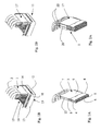
- Figs. 1A and 1B show by way of example a connector wafer 1 which is used to assemble different embodiments of the connector of the invention as shown in Figs. 2-4 .
- the connector wafer 1 is adapted to be used as a connector wafer for a cable connector accommodating in this example four cables 2, each cable 2 having a differential pair of signal conductors and one or two ground conductors not further shown.
- the signal conductors and ground conductors are connected to contact elements accommodated in a housing 3 of the connector wafer 1.
- the housing 3 has opposite side edges 4, an insertion side 5 with apertures 6 allowing access to the contact elements accommodated in the housing 3.
- the housing has a backside 7 and opposite main faces 8,9.
- the cables 2 are introduced into the housing 3 from the backside 7.
- the connector wafer 1 can be used on its own as cable connector and can be introduced into the housing 10 of a second connector 11 which can be mounted on a printed circuit board not further shown.
- the second housing 11 comprises a bottom wall 12 and two opposite upstanding sidewalls 13,14 determining a receiving space 15 in which a number of contact elements 16 can be seen.
- the connector wafer 1 can be inserted into the receiving space 15 with its insertion side 5 to interconnect the contact elements of the connector wafer 1 and the connector elements 16 of the second connector 11.
- Figs. 2-4 show three different connectors 17,18 and 19 as embodiments of the connector of the invention.
- the connectors 17-19 comprise two, four, and eight connector wafers 1, respectively.
- the connector wafers 1 are coupled or interconnected at both side edges 4 by coupling pieces 20 having a different length in the embodiments of Figs. 2 , 3 and 4 , respectively. It is possible to use one coupling piece 20 at one side edge only. However it is preferred to use coupling pieces at both side edges.
- the connectors 17-19 can be inserted into a second connector 11, wherein the construction and pitch of the connector wafers 1 in the connector 17-19 is such that two or more connectors 17-19 can be inserted into one second connector 11.
- Figs. 6A-6C show different views of the coupling piece 20 of the connector 17 shown in Fig. 2 .
- This coupling piece comprises two adjacent coupling means 21 co-operating with corresponding coupling means 22 of a connector wafer 1.
- the coupling means 21 of the coupling means 20 are made as coupling slots with a dovetail-shaped cross-section as can be seen in Figs. 6A-6C .
- the coupling means 22 of the connector wafers 1 are made as coupling ridges on both side edges 4 and these coupling ridges 22 have a corresponding dovetail-shaped cross-section so that a firm interconnection between the coupling pieces 20 and the connector wafers 1 is provided.
- the coupling pieces 20 can be slid in the connector wafers 1 from the backside towards the insertion side or vice versa.
- relatively long co-operating surfaces of slots 21 and ridges 22 are obtained providing an accurate alignment of the connector wafers 1.
- the left coupling slot 21 is offset from the adjacent coupling slot 21 so that the adjacent connector wafers 1 are positioned offset and in this manner each column of contact elements is offset from an adjacent column of contact elements.
- cross-talk can be reduced in this manner.
- the present invention relates to providing a coupling piece 20 with adjacent coupling means 21, wherein each coupling means 21 is offset from an adjacent coupling means 21.
- manufacturing a connector with a desired number of connector wafers 1, wherein each connector wafer 1 is offset from an adjacent connector wafer 1, thereby providing offset adjacent columns of contact elements, is relatively simple.
- a standard coupling piece 20 is shown having eight successive coupling slots 21 which coupling slots just as in the coupling piece of Fig. 6 are provided in an offset manner so that each coupling slot 21 is offset from an adjacent coupling slot 21. If a connector 18 with four connector wafers 1 has to be assembled, the coupling piece 20 of Fig. 5 is broken in two parts, each part having four coupling slots 21. In the same manner a coupling piece with two up to seven coupling slots 21 can be obtained by removing one up to six coupling slots 21. Removing a part of the coupling piece 20 of Fig.
- breaking locations 23 are obtained by two opposite grooves 24 which are preferably V-shaped. If desired a coupling piece with breaking locations can be provided with non-offset coupling means so that the columns of contact elements of the coupled connector wafers will be aligned in a usual manner.
- all connectors 17-19 have the same column pitch in such a manner that the facing main faces 8,9 of adjacent connector wafers 1 are contacting each other.
- a different coupling piece 20 can be provided having a different pitch of adjacent coupling slots 21.
- the pitch of the coupling slots 21 determines the column pitch of the assembled connector, connectors with any desired column pitch can be manufactured by providing suitable coupling pieces 20.
- the coupling slots provide for a polarisation/coding of adjacent connector wafers as the left-hand slot 21 has a different size as the right-hand slot 21. In this manner it can be guaranteed that adjacent connector wafers 1 are used having a different order of signal and ground contact elements as described in US-A-6 652 318 .
- the coupling piece 20 allows the use of extended coupling pieces, i.e. a coupling piece which extends substantially from the backside 7 up to the insertion side 5 of the connector wafers 1.
- Figs. 7A and 7B show a coupling piece 25 having such extensions 26,27, wherein the coupling slots 21 extend along the full length of the coupling piece 25.
- the extensions 26,27 can be provided with polarisation and coding elements 28,29.
- connectors can be manufactured with any desired type of polarisation and coding elements. Further, it is possible to change the polarisation/coding elements of a connector even after completion of the connector.
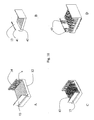
- Figs. 8 and 9 show a different embodiment of the connector of the invention indicated with reference numeral 30.
- This connector 30 comprises two connector wafers 31 which are mainly made in the same manner as the connector wafers 1.
- the connector wafers 31 are interconnected by two coupling pieces 32 having adjacent offset coupling means 33 co-operating with corresponding coupling means 34 provided on the opposite side edges 4 of the connector wafers 31.
- Figs. 8A and 8B show the assembled connector 30, whereas in Figs. 9A and 9B the coupling pieces 32 are shown separated from the connector wafers 31.
- the coupling pieces 32 located close to the insertion side 5 of the connector wafers 31 are provided with polarisation/coding elements 35.
- the coupling piece 32 is mounted on the connector wafers 31 by snapping/clicking the coupling piece onto the connector wafers 31 instead of sliding as in the above-described embodiments.
- the coupling means 33 of the coupling piece 32 comprises dovetail edges 36 co-operating with corresponding dovetail edges 37 of the coupling means of the connector wafers 31.
- Further alignment protrusions 38 are provided on the coupling piece 32 co-operating with alignment recesses 39 of the connector wafers 31.
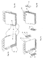
- Figs. 10A-10D show a second connector according to the invention indicated by reference numeral 40.
- connector 40 comprises a bottom wall 12 and opposite upstanding sidewalls 13,14.
- upstanding sidewall 13 is a flat sidewall having mounting recesses 41 at its upper side and adjacent mounting recesses 42 in the bottom wall 12.
- polarisation/coding elements 43 can be mounted adjacent to the sidewall 13 as schematically shown in Figs. 10C and 10D .
- the detachably mounted polarisation/coding elements allow to assemble a connector 40 with any desired type of polarisation/coding by providing suitable elements 43.
- Figs. 11 and 12 show an embodiment of the connector 40 with two polarisation/coding elements 43 and a connector 19 inserted into the connector 40.
- a latching element 44 is mounted in between the two coding elements 43 to provide an active latching of the connector 19 in the connector 40.
- the connector 40 with latching element 43 is further described in a co-pending patent application of the same applicant with the same filing date. For a further description reference is made to this co-pending application.
- Figs. 13A and 13B show a further embodiment of the connector of the invention indicated by reference numeral 45.
- Fig. 13A shows the connector 45 as assembled, however without cables, and
- Fig. 13B shows the connector wafers 1 separately from the two coupling pieces 46 used.
- the coupling pieces 46 each are provided with the same coupling slots 21 as the coupling piece 20 provided in an offset manner and having different sizes as described above.
- the coupling pieces 46 are provided with cover parts 47 and 48 enclosing the main faces 8,9 and the backside 7 of the connector wafers 1.
- This embodiment shows that the design of the coupling piece 20 shown in Figs. 5 and 6 allows the coupling piece to be provided with further parts to complete the connector in any desired manner.
Landscapes
- Details Of Connecting Devices For Male And Female Coupling (AREA)
- Connector Housings Or Holding Contact Members (AREA)
- Coupling Device And Connection With Printed Circuit (AREA)
Claims (16)
- Connecteur, comprenant une pluralité de tranches de connecteur (1) accouplées par un élément d'accouplement (20), chaque tranche de connecteur comprenant un logement (3) recevant une colonne d'éléments de contact, ledit logement comportant des bords latéraux (4) opposés, un côté d'insertion (5) comportant des ouvertures (6) permettant d'accéder aux éléments de contact, un côté arrière (7), et des faces principales (8, 9) opposées, dans lequel ledit élément d'accouplement est pourvu de moyens d'accouplement pour chaque tranche de connecteur venant en prise avec les moyens d'accouplement correspondants d'une tranche de connecteur, caractérisé en ce que chaque moyen d'accouplement (21, 22) de l'élément d'accouplement (20) venant en prise avec une tranche de connecteur (1) est décalé par rapport à un moyen d'accouplement adjacent venant en prise avec une tranche de connecteur adjacente pour réaliser des colonnes décalées d'éléments de contact.
- Connecteur selon la revendication 1, dans lequel les moyens d'accouplement (21, 22) des tranches de connecteur sont prévus en tant qu'arête d'accouplement (22) sur un bord latéral (4) ou les deux bords latéraux de la tranche de connecteur s'étendant dans la direction s'étendant depuis le côté d'insertion (5) vers le côté arrière (7), et dans lequel les moyens d'accouplement de l'élément d'accouplement sont prévus en tant que fente d'accouplement (21) adaptée pour recevoir une arête d'accouplement de tranche de connecteur, les fentes et les arêtes d'accouplement ayant de préférence une section en queue d'aronde.
- Connecteur selon la revendication 2, dans lequel l'élément d'accouplement (20) s'étend jusqu'au côté d'insertion (5) des tranches de connecteur, dans lequel le côté externe de l'élément d'accouplement est pourvu d'éléments de polarisation et/ou d'éléments de codage (28, 29) à son extrémité d'insertion.
- Connecteur selon la revendication 3, dans lequel les arêtes (22) et les fentes (21) d'accouplement s'étendent jusqu'au côté d'insertion des tranches de connecteur.
- Connecteur selon l'une quelconque des revendications précédentes, dans lequel ledit élément d'accouplement (20) est pourvu d'emplacements de rupture entre les moyens d'accouplement décalés.
- Connecteur selon la revendication 5, dans lequel ledit élément d'accouplement est pourvu de rainures opposées, de préférence en forme de V, réalisant lesdits emplacements de rupture.
- Connecteur selon l'une quelconque des revendications précédentes, dans lequel ledit élément d'accouplement, de son côté comportant des moyens d'accouplement décalés, est pourvu de moyens de polarisation coopérant avec les moyens de polarisation desdites tranches de connecteur.
- Connecteur selon la revendication 7, dans lequel lesdits moyens de polarisation de l'élément d'accouplement et des tranches de connecteur sont réalisés en tant que dites fentes d'accouplement et arêtes d'accouplement ayant différentes tailles.
- Connecteur selon l'une quelconque des revendications précédentes, dans lequel ledit élément d'accouplement est pourvu d'une section de recouvrement entourant au moins une partie de la face principale et/ou du côté arrière du connecteur.
- Système d'assemblage de connecteur pour assembler un connecteur, comprenant des tranches de connecteur (1) et des éléments d'accouplement (20) comportant un nombre maximum de moyens d'accouplement (21) décalés successifs, dans lequel l'élément d'accouplement est pourvu d'emplacements de rupture (23) entre les moyens d'accouplement décalés pour permettre l'assemblage de connecteurs comportant un nombre variable de colonnes d'éléments de contact.
- Système d'assemblage de connecteur pour assembler un connecteur selon la revendication 10, comprenant différents éléments d'accouplement comportant des moyens d'accouplement décalés successifs espacés selon un pas différent pour permettre l'assemblage de connecteurs avec différents pas de colonnes.
- Procédé d'assemblage d'un connecteur, comprenant des étapes au cours desquelles on prévoit une pluralité de tranches de connecteur, chaque tranche de connecteur comportant un logement avec des bords latéraux opposés, au moins un bord comportant des moyens d'accouplement, on prévoit un élément d'accouplement comportant un certain nombre de moyens d'accouplement successifs, et on accouple un nombre souhaité de tranches de connecteur en utilisant au moins un élément d'accouplement, caractérisé en ce que l'élément d'accouplement est pourvu de moyens d'accouplement décalés successifs pour venir en prise avec les moyens d'accouplement de tranches de connecteur successives, dans lequel les tranches de connecteur adjacentes sont positionnées de manière décalée en interconnectant les tranches de connecteur au moyen de l'élément d'accouplement.
- Procédé selon la revendication 12, dans lequel l'élément d'accouplement comporte un nombre maximum de moyens d'accouplement décalés successifs séparés par des emplacements de rupture, dans lequel l'élément d'accouplement est ajusté au nombre souhaité de tranches de connecteur en retirant une partie de l'élément d'accouplement en rompant l'élément d'accouplement à un emplacement de rupture correspondant.
- Procédé selon la revendication 12 ou 13, dans lequel l'élément d'accouplement est glissé sur le nombre souhaité de tranches de connecteur dans une direction s'étendant depuis le côté arrière des tranches de connecteur vers le côté d'insertion des tranches de connecteur.
- Procédé selon la revendication 12, 13 ou 14, dans lequel des éléments d'accouplement avec un pas différent d'éléments d'accouplement décalés successifs sont prévus et un élément d'accouplement avec un pas souhaité des moyens d'accouplement est sélectionné et glissé sur un certain nombre de tranches de connecteur pour obtenir un connecteur avec un pas de colonnes souhaité.
- Elément d'accouplement comprenant un certain nombre de moyens d'accouplement successifs adaptés pour coopérer avec des moyens d'accouplement complémentaires de tranches de connecteur successives, dans lequel deux moyens d'accouplement successifs de l'élément d'accouplement sont décalés l'un par rapport à l'autre.
Applications Claiming Priority (2)
| Application Number | Priority Date | Filing Date | Title |
|---|---|---|---|
| NL1026502A NL1026502C2 (nl) | 2004-06-25 | 2004-06-25 | Connector, connector-samenstelsysteem en werkwijze voor het samenstellen van een connector. |
| PCT/EP2005/006621 WO2006002793A1 (fr) | 2004-06-25 | 2005-06-20 | Connecteur, systeme d'assemblage de connecteur et procede d'assemblage d'un connecteur |
Publications (2)
| Publication Number | Publication Date |
|---|---|
| EP1763910A1 EP1763910A1 (fr) | 2007-03-21 |
| EP1763910B1 true EP1763910B1 (fr) | 2010-03-31 |
Family
ID=34972398
Family Applications (1)
| Application Number | Title | Priority Date | Filing Date |
|---|---|---|---|
| EP05760078A Expired - Lifetime EP1763910B1 (fr) | 2004-06-25 | 2005-06-20 | Connecteur, systeme d'assemblage de connecteur et procede d'assemblage d'un connecteur |
Country Status (10)
| Country | Link |
|---|---|
| US (1) | US7422490B2 (fr) |
| EP (1) | EP1763910B1 (fr) |
| JP (1) | JP4856065B2 (fr) |
| KR (1) | KR20070059051A (fr) |
| CN (1) | CN1977426B (fr) |
| AT (1) | ATE463060T1 (fr) |
| CA (1) | CA2570530A1 (fr) |
| DE (1) | DE602005020291D1 (fr) |
| NL (1) | NL1026502C2 (fr) |
| WO (1) | WO2006002793A1 (fr) |
Families Citing this family (18)
| Publication number | Priority date | Publication date | Assignee | Title |
|---|---|---|---|---|
| CN101496231B (zh) | 2006-05-23 | 2012-05-30 | Fci公司 | 电连接器、连接器基板和联接件及组装连接器的工具 |
| US7709753B1 (en) * | 2007-11-07 | 2010-05-04 | Russo Michael H | Electrical wiring block system |
| US7762846B1 (en) * | 2009-09-15 | 2010-07-27 | Tyco Electronics Corporation | Connector assembly having a back shell |
| CN102823073A (zh) | 2010-02-01 | 2012-12-12 | 3M创新有限公司 | 电连接器和组件 |
| WO2012050628A1 (fr) | 2010-10-13 | 2012-04-19 | 3M Innovative Properties Company | Ensemble et système de connecteur électrique |
| US8435074B1 (en) * | 2011-11-14 | 2013-05-07 | Airborn, Inc. | Low-profile right-angle electrical connector assembly |
| US8784122B2 (en) | 2011-11-14 | 2014-07-22 | Airborn, Inc. | Low-profile right-angle electrical connector assembly |
| JP2013137922A (ja) * | 2011-12-28 | 2013-07-11 | Tyco Electronics Japan Kk | 電気コネクタ |
| EP2854239B1 (fr) * | 2013-09-25 | 2019-11-13 | Virginia Panel Corporation | Module de données à grande vitesse pour dispositif d'interconnexion de cycle de vie élevé |
| US9362638B2 (en) * | 2014-09-03 | 2016-06-07 | Amphenol Corporation | Overmolded contact wafer and connector |
| TW201613203A (en) * | 2014-09-29 | 2016-04-01 | Foxconn Interconnect Technology Ltd | Electrical connector assembly and assembling method of the same |
| CN107592948B (zh) * | 2015-05-01 | 2019-08-16 | 3M创新有限公司 | 连接器组件 |
| CN205303726U (zh) * | 2015-12-04 | 2016-06-08 | 富士康(昆山)电脑接插件有限公司 | 线缆连接器 |
| DE102016213286A1 (de) * | 2016-07-20 | 2018-01-25 | Harting Electric Gmbh & Co. Kg | Mehrteiliger Halterahmen, Konfektionier- und Bestückungsverfahren |
| JP7353035B2 (ja) * | 2018-12-26 | 2023-09-29 | スリーエム イノベイティブ プロパティズ カンパニー | 積層型ワイヤマウントウェハコネクタ及びコネクタアセンブリ |
| CN110336156B (zh) * | 2019-06-29 | 2021-02-26 | 苏州浪潮智能科技有限公司 | 一种双体连接器 |
| US11218838B2 (en) | 2019-10-31 | 2022-01-04 | Snap Inc. | Focused map-based context information surfacing |
| CN112350095B (zh) * | 2020-11-17 | 2022-08-16 | 深圳市方向电子股份有限公司 | 一种高速传输线对板连接器 |
Family Cites Families (30)
| Publication number | Priority date | Publication date | Assignee | Title |
|---|---|---|---|---|
| US3325771A (en) * | 1964-04-09 | 1967-06-13 | Elco Corp | Electrical connector module with adjustable polarization |
| US4984992A (en) * | 1989-11-01 | 1991-01-15 | Amp Incorporated | Cable connector with a low inductance path |
| DE9311781U1 (de) * | 1992-10-29 | 1993-09-30 | Siemens AG, 80333 München | Kabelstecker für vieladrige Kabel |
| US5312276A (en) * | 1993-03-19 | 1994-05-17 | The Whitaker Corporation | Connector polarizing structure |
| NL9302007A (nl) * | 1993-11-19 | 1995-06-16 | Framatome Connectors Belgium | Connector voor afgeschermde kabels. |
| NL9302005A (nl) * | 1993-11-19 | 1995-06-16 | Framatome Connectors Belgium | Connector voor afgeschermde kabels. |
| NL9400321A (nl) * | 1994-03-03 | 1995-10-02 | Framatome Connectors Belgium | Connector voor een kabel voor hoogfrequente signalen. |
| US5387130A (en) * | 1994-03-29 | 1995-02-07 | The Whitaker Corporation | Shielded electrical cable assembly with shielding back shell |
| DE4425466A1 (de) * | 1994-07-19 | 1996-01-25 | Thomas & Betts Gmbh | Kabel-Steckverbinder |
| US5634822A (en) * | 1994-11-14 | 1997-06-03 | Augat Inc. | Miniature telephone jack and rack system |
| US5997361A (en) * | 1997-06-30 | 1999-12-07 | Litton Systems, Inc. | Electronic cable connector |
| US5961355A (en) * | 1997-12-17 | 1999-10-05 | Berg Technology, Inc. | High density interstitial connector system |
| HUP0105197A2 (en) * | 1999-01-15 | 2002-05-29 | Adc Telecommunications Inc | Telecommunications jack assembly |
| JP2001015223A (ja) * | 1999-06-25 | 2001-01-19 | Nec Corp | 汎用コネクタおよびその結合方法 |
| JP2001015214A (ja) * | 1999-06-29 | 2001-01-19 | Nec Corp | シールドコネクタと受け側コネクタの結合部構造 |
| US6361374B1 (en) * | 2000-02-29 | 2002-03-26 | Molex Incorporated | Connector module retainer especially suitable for wafer connectors and connector assembly utilizing same |
| US6371788B1 (en) * | 2000-05-19 | 2002-04-16 | Molex Incorporated | Wafer connection latching assembly |
| US6352452B1 (en) * | 2000-07-12 | 2002-03-05 | Molex Incorporated And Tellabs Operations, Inc. | Connector module polarization assembly |
| NL1019122C2 (nl) * | 2001-10-05 | 2003-04-08 | Framatome Connectors Int | Connectorsamenstel, vergrendelclip en werkwijze voor het samenstellen van een connector. |
| US6652318B1 (en) * | 2002-05-24 | 2003-11-25 | Fci Americas Technology, Inc. | Cross-talk canceling technique for high speed electrical connectors |
| US6837720B2 (en) * | 2001-11-27 | 2005-01-04 | Sun Microsystems, Inc. | Connector for electrically coupling one or more devices in a processor-based system |
| US6979215B2 (en) * | 2001-11-28 | 2005-12-27 | Molex Incorporated | High-density connector assembly with flexural capabilities |
| KR100434230B1 (ko) * | 2002-03-26 | 2004-06-04 | 한국몰렉스 주식회사 | 고속통신용 케이블 커넥터 어셈블리 |
| JP4091603B2 (ja) * | 2002-06-21 | 2008-05-28 | モレックス インコーポレーテッド | モジュール構造を有するインピーダンス調整された高密度コネクタ |
| US6685510B1 (en) * | 2002-10-22 | 2004-02-03 | Hon Hai Precision Ind. Co., Ltd. | Electrical cable connector |
| US6743050B1 (en) * | 2002-12-10 | 2004-06-01 | Hon Hai Precision Ind. Co., Ltd. | Cable assembly with latch mechanism |
| US6926553B2 (en) * | 2003-06-19 | 2005-08-09 | Hon Hai Precision Ind. Co., Ltd. | Cable assembly with improved grounding means |
| US6857912B2 (en) * | 2003-06-25 | 2005-02-22 | Hon Hai Precision Ind. Co., Ltd | Cable assembly with internal circuit modules |
| US6814620B1 (en) * | 2003-07-01 | 2004-11-09 | Hon Hai Precision Ind. Co. Ltd. | Electrical connector |
| US6739910B1 (en) * | 2003-07-11 | 2004-05-25 | Hon Hai Precision Ind. Co., Ltd. | Cable assembly with internal circuit modules |
-
2004
- 2004-06-25 NL NL1026502A patent/NL1026502C2/nl not_active IP Right Cessation
-
2005
- 2005-06-20 EP EP05760078A patent/EP1763910B1/fr not_active Expired - Lifetime
- 2005-06-20 DE DE602005020291T patent/DE602005020291D1/de not_active Expired - Lifetime
- 2005-06-20 US US11/630,292 patent/US7422490B2/en not_active Expired - Fee Related
- 2005-06-20 JP JP2007517172A patent/JP4856065B2/ja not_active Expired - Fee Related
- 2005-06-20 CA CA002570530A patent/CA2570530A1/fr not_active Abandoned
- 2005-06-20 CN CN2005800212593A patent/CN1977426B/zh not_active Expired - Fee Related
- 2005-06-20 KR KR1020077001698A patent/KR20070059051A/ko not_active Withdrawn
- 2005-06-20 WO PCT/EP2005/006621 patent/WO2006002793A1/fr not_active Ceased
- 2005-06-20 AT AT05760078T patent/ATE463060T1/de not_active IP Right Cessation
Also Published As
| Publication number | Publication date |
|---|---|
| CN1977426A (zh) | 2007-06-06 |
| KR20070059051A (ko) | 2007-06-11 |
| EP1763910A1 (fr) | 2007-03-21 |
| US20080026642A1 (en) | 2008-01-31 |
| JP4856065B2 (ja) | 2012-01-18 |
| CN1977426B (zh) | 2011-11-30 |
| JP2008503861A (ja) | 2008-02-07 |
| CA2570530A1 (fr) | 2006-01-12 |
| DE602005020291D1 (de) | 2010-05-12 |
| WO2006002793A1 (fr) | 2006-01-12 |
| ATE463060T1 (de) | 2010-04-15 |
| US7422490B2 (en) | 2008-09-09 |
| NL1026502C2 (nl) | 2005-12-28 |
Similar Documents
| Publication | Publication Date | Title |
|---|---|---|
| US7422490B2 (en) | Connector, connector assembling system and method of assembling a connector | |
| US5525066A (en) | Connector for a cable for high frequency signals | |
| US6890214B2 (en) | Multi-sequenced contacts from single lead frame | |
| US6439928B1 (en) | High density connector for balanced transmission lines | |
| EP0627788B1 (fr) | Ensemble de connexion | |
| EP1382094B1 (fr) | Ensemble connecteur electrique pour l'assemblage orthogonal de cartes a circuit | |
| CN1960063B (zh) | 垂直对接连接器 | |
| RU2174275C2 (ru) | Подсоединительная колодка для высокоскоростной передачи информации | |
| JP4521834B2 (ja) | コネクタ | |
| US7104808B2 (en) | Mating extender for electrically connecting with two electrical connectors | |
| JP2904424B2 (ja) | 基板用コネクタ及びそれに用いるタインプレート | |
| JP2021044080A (ja) | コネクタおよびコネクタの製造方法 | |
| EP1263087B1 (fr) | Bloc à bornes et connecteur pour câbles | |
| US5199906A (en) | Electrical connector | |
| EP0342873B1 (fr) | Connecteur pour le montage sur une surface | |
| US6089925A (en) | Modular electrical connector having electrical contact modules | |
| CN122073348A (zh) | 电连接器,电连接器组件及电连接器系统 | |
| EP0399074A1 (fr) | Connecteur électrique | |
| JP2009518786A (ja) | ケーブルコネクタ及びヘッダ | |
| JPH11273807A (ja) | 基板用コネクタ | |
| HK1136697A (en) | Plug-in connector for circuit boards | |
| KR20020075683A (ko) | 접속커버를 구비한 모듈라 잭 |
Legal Events
| Date | Code | Title | Description |
|---|---|---|---|
| PUAI | Public reference made under article 153(3) epc to a published international application that has entered the european phase |
Free format text: ORIGINAL CODE: 0009012 |
|
| 17P | Request for examination filed |
Effective date: 20070125 |
|
| AK | Designated contracting states |
Kind code of ref document: A1 Designated state(s): AT BE BG CH CY CZ DE DK EE ES FI FR GB GR HU IE IS IT LI LT LU MC NL PL PT RO SE SI SK TR |
|
| DAX | Request for extension of the european patent (deleted) | ||
| 17Q | First examination report despatched |
Effective date: 20071218 |
|
| 111Z | Information provided on other rights and legal means of execution |
Free format text: AT BE BG CH CY CZ DE DK EE ES FI FR GB GR HU IE IS IT LT LU MC NL PL PT RO SE SI SK TR Effective date: 20090223 |
|
| GRAP | Despatch of communication of intention to grant a patent |
Free format text: ORIGINAL CODE: EPIDOSNIGR1 |
|
| GRAS | Grant fee paid |
Free format text: ORIGINAL CODE: EPIDOSNIGR3 |
|
| GRAA | (expected) grant |
Free format text: ORIGINAL CODE: 0009210 |
|
| RAP1 | Party data changed (applicant data changed or rights of an application transferred) |
Owner name: FCI |
|
| AK | Designated contracting states |
Kind code of ref document: B1 Designated state(s): AT BE BG CH CY CZ DE DK EE ES FI FR GB GR HU IE IS IT LI LT LU MC NL PL PT RO SE SI SK TR |
|
| REG | Reference to a national code |
Ref country code: CH Ref legal event code: EP Ref country code: GB Ref legal event code: FG4D |
|
| REG | Reference to a national code |
Ref country code: IE Ref legal event code: FG4D |
|
| REF | Corresponds to: |
Ref document number: 602005020291 Country of ref document: DE Date of ref document: 20100512 Kind code of ref document: P |
|
| REG | Reference to a national code |
Ref country code: SE Ref legal event code: TRGR |
|
| REG | Reference to a national code |
Ref country code: NL Ref legal event code: VDEP Effective date: 20100331 |
|
| PG25 | Lapsed in a contracting state [announced via postgrant information from national office to epo] |
Ref country code: LT Free format text: LAPSE BECAUSE OF FAILURE TO SUBMIT A TRANSLATION OF THE DESCRIPTION OR TO PAY THE FEE WITHIN THE PRESCRIBED TIME-LIMIT Effective date: 20100331 |
|
| PGFP | Annual fee paid to national office [announced via postgrant information from national office to epo] |
Ref country code: FI Payment date: 20100526 Year of fee payment: 6 |
|
| LTIE | Lt: invalidation of european patent or patent extension |
Effective date: 20100331 |
|
| PG25 | Lapsed in a contracting state [announced via postgrant information from national office to epo] |
Ref country code: PL Free format text: LAPSE BECAUSE OF FAILURE TO SUBMIT A TRANSLATION OF THE DESCRIPTION OR TO PAY THE FEE WITHIN THE PRESCRIBED TIME-LIMIT Effective date: 20100331 Ref country code: SI Free format text: LAPSE BECAUSE OF FAILURE TO SUBMIT A TRANSLATION OF THE DESCRIPTION OR TO PAY THE FEE WITHIN THE PRESCRIBED TIME-LIMIT Effective date: 20100331 Ref country code: AT Free format text: LAPSE BECAUSE OF FAILURE TO SUBMIT A TRANSLATION OF THE DESCRIPTION OR TO PAY THE FEE WITHIN THE PRESCRIBED TIME-LIMIT Effective date: 20100331 |
|
| PG25 | Lapsed in a contracting state [announced via postgrant information from national office to epo] |
Ref country code: RO Free format text: LAPSE BECAUSE OF FAILURE TO SUBMIT A TRANSLATION OF THE DESCRIPTION OR TO PAY THE FEE WITHIN THE PRESCRIBED TIME-LIMIT Effective date: 20100331 Ref country code: NL Free format text: LAPSE BECAUSE OF FAILURE TO SUBMIT A TRANSLATION OF THE DESCRIPTION OR TO PAY THE FEE WITHIN THE PRESCRIBED TIME-LIMIT Effective date: 20100331 Ref country code: ES Free format text: LAPSE BECAUSE OF FAILURE TO SUBMIT A TRANSLATION OF THE DESCRIPTION OR TO PAY THE FEE WITHIN THE PRESCRIBED TIME-LIMIT Effective date: 20100712 Ref country code: EE Free format text: LAPSE BECAUSE OF FAILURE TO SUBMIT A TRANSLATION OF THE DESCRIPTION OR TO PAY THE FEE WITHIN THE PRESCRIBED TIME-LIMIT Effective date: 20100331 Ref country code: CY Free format text: LAPSE BECAUSE OF FAILURE TO SUBMIT A TRANSLATION OF THE DESCRIPTION OR TO PAY THE FEE WITHIN THE PRESCRIBED TIME-LIMIT Effective date: 20100331 Ref country code: BE Free format text: LAPSE BECAUSE OF FAILURE TO SUBMIT A TRANSLATION OF THE DESCRIPTION OR TO PAY THE FEE WITHIN THE PRESCRIBED TIME-LIMIT Effective date: 20100331 |
|
| RAP2 | Party data changed (patent owner data changed or rights of a patent transferred) |
Owner name: FCI |
|
| PG25 | Lapsed in a contracting state [announced via postgrant information from national office to epo] |
Ref country code: SK Free format text: LAPSE BECAUSE OF FAILURE TO SUBMIT A TRANSLATION OF THE DESCRIPTION OR TO PAY THE FEE WITHIN THE PRESCRIBED TIME-LIMIT Effective date: 20100331 Ref country code: CZ Free format text: LAPSE BECAUSE OF FAILURE TO SUBMIT A TRANSLATION OF THE DESCRIPTION OR TO PAY THE FEE WITHIN THE PRESCRIBED TIME-LIMIT Effective date: 20100331 Ref country code: IS Free format text: LAPSE BECAUSE OF FAILURE TO SUBMIT A TRANSLATION OF THE DESCRIPTION OR TO PAY THE FEE WITHIN THE PRESCRIBED TIME-LIMIT Effective date: 20100731 |
|
| PG25 | Lapsed in a contracting state [announced via postgrant information from national office to epo] |
Ref country code: PT Free format text: LAPSE BECAUSE OF FAILURE TO SUBMIT A TRANSLATION OF THE DESCRIPTION OR TO PAY THE FEE WITHIN THE PRESCRIBED TIME-LIMIT Effective date: 20100802 Ref country code: MC Free format text: LAPSE BECAUSE OF NON-PAYMENT OF DUE FEES Effective date: 20100630 Ref country code: DK Free format text: LAPSE BECAUSE OF FAILURE TO SUBMIT A TRANSLATION OF THE DESCRIPTION OR TO PAY THE FEE WITHIN THE PRESCRIBED TIME-LIMIT Effective date: 20100331 |
|
| REG | Reference to a national code |
Ref country code: CH Ref legal event code: PL |
|
| PLBE | No opposition filed within time limit |
Free format text: ORIGINAL CODE: 0009261 |
|
| STAA | Information on the status of an ep patent application or granted ep patent |
Free format text: STATUS: NO OPPOSITION FILED WITHIN TIME LIMIT |
|
| GBPC | Gb: european patent ceased through non-payment of renewal fee |
Effective date: 20100630 |
|
| 26N | No opposition filed |
Effective date: 20110104 |
|
| REG | Reference to a national code |
Ref country code: FR Ref legal event code: ST Effective date: 20110228 |
|
| PG25 | Lapsed in a contracting state [announced via postgrant information from national office to epo] |
Ref country code: IT Free format text: LAPSE BECAUSE OF FAILURE TO SUBMIT A TRANSLATION OF THE DESCRIPTION OR TO PAY THE FEE WITHIN THE PRESCRIBED TIME-LIMIT Effective date: 20100331 |
|
| PG25 | Lapsed in a contracting state [announced via postgrant information from national office to epo] |
Ref country code: CH Free format text: LAPSE BECAUSE OF NON-PAYMENT OF DUE FEES Effective date: 20100630 Ref country code: LI Free format text: LAPSE BECAUSE OF NON-PAYMENT OF DUE FEES Effective date: 20100630 Ref country code: IE Free format text: LAPSE BECAUSE OF NON-PAYMENT OF DUE FEES Effective date: 20100620 |
|
| PG25 | Lapsed in a contracting state [announced via postgrant information from national office to epo] |
Ref country code: FR Free format text: LAPSE BECAUSE OF NON-PAYMENT OF DUE FEES Effective date: 20100630 |
|
| PG25 | Lapsed in a contracting state [announced via postgrant information from national office to epo] |
Ref country code: GB Free format text: LAPSE BECAUSE OF NON-PAYMENT OF DUE FEES Effective date: 20100630 |
|
| PG25 | Lapsed in a contracting state [announced via postgrant information from national office to epo] |
Ref country code: FI Free format text: LAPSE BECAUSE OF NON-PAYMENT OF DUE FEES Effective date: 20110620 |
|
| REG | Reference to a national code |
Ref country code: DE Ref legal event code: R081 Ref document number: 602005020291 Country of ref document: DE Owner name: FCI ASIA PTE. LTD, SG Free format text: FORMER OWNER: FCI, VERSAILLES, FR Effective date: 20120419 Ref country code: DE Ref legal event code: R081 Ref document number: 602005020291 Country of ref document: DE Owner name: FCI, FR Free format text: FORMER OWNER: FCI, VERSAILLES, FR Effective date: 20120419 |
|
| PG25 | Lapsed in a contracting state [announced via postgrant information from national office to epo] |
Ref country code: BG Free format text: LAPSE BECAUSE OF FAILURE TO SUBMIT A TRANSLATION OF THE DESCRIPTION OR TO PAY THE FEE WITHIN THE PRESCRIBED TIME-LIMIT Effective date: 20100331 Ref country code: HU Free format text: LAPSE BECAUSE OF FAILURE TO SUBMIT A TRANSLATION OF THE DESCRIPTION OR TO PAY THE FEE WITHIN THE PRESCRIBED TIME-LIMIT Effective date: 20101001 Ref country code: LU Free format text: LAPSE BECAUSE OF NON-PAYMENT OF DUE FEES Effective date: 20100620 |
|
| PG25 | Lapsed in a contracting state [announced via postgrant information from national office to epo] |
Ref country code: TR Free format text: LAPSE BECAUSE OF FAILURE TO SUBMIT A TRANSLATION OF THE DESCRIPTION OR TO PAY THE FEE WITHIN THE PRESCRIBED TIME-LIMIT Effective date: 20100331 |
|
| PG25 | Lapsed in a contracting state [announced via postgrant information from national office to epo] |
Ref country code: BG Free format text: LAPSE BECAUSE OF FAILURE TO SUBMIT A TRANSLATION OF THE DESCRIPTION OR TO PAY THE FEE WITHIN THE PRESCRIBED TIME-LIMIT Effective date: 20100630 |
|
| PG25 | Lapsed in a contracting state [announced via postgrant information from national office to epo] |
Ref country code: GR Free format text: LAPSE BECAUSE OF FAILURE TO SUBMIT A TRANSLATION OF THE DESCRIPTION OR TO PAY THE FEE WITHIN THE PRESCRIBED TIME-LIMIT Effective date: 20100331 |
|
| REG | Reference to a national code |
Ref country code: DE Ref legal event code: R081 Ref document number: 602005020291 Country of ref document: DE Owner name: FCI ASIA PTE. LTD, SG Free format text: FORMER OWNER: FCI, GUYANCOURT, FR Effective date: 20150113 |
|
| PGFP | Annual fee paid to national office [announced via postgrant information from national office to epo] |
Ref country code: DE Payment date: 20160629 Year of fee payment: 12 |
|
| REG | Reference to a national code |
Ref country code: DE Ref legal event code: R119 Ref document number: 602005020291 Country of ref document: DE |
|
| REG | Reference to a national code |
Ref country code: SE Ref legal event code: EUG |
|
| PG25 | Lapsed in a contracting state [announced via postgrant information from national office to epo] |
Ref country code: SE Free format text: LAPSE BECAUSE OF NON-PAYMENT OF DUE FEES Effective date: 20170621 |
|
| PG25 | Lapsed in a contracting state [announced via postgrant information from national office to epo] |
Ref country code: DE Free format text: LAPSE BECAUSE OF NON-PAYMENT OF DUE FEES Effective date: 20180103 |
|
| PGFP | Annual fee paid to national office [announced via postgrant information from national office to epo] |
Ref country code: SE Payment date: 20190627 Year of fee payment: 15 |