EP1765739B1 - Substrat transparent comprenant un empilement antireflechissant de couches - Google Patents
Substrat transparent comprenant un empilement antireflechissant de couches Download PDFInfo
- Publication number
- EP1765739B1 EP1765739B1 EP04766863.7A EP04766863A EP1765739B1 EP 1765739 B1 EP1765739 B1 EP 1765739B1 EP 04766863 A EP04766863 A EP 04766863A EP 1765739 B1 EP1765739 B1 EP 1765739B1
- Authority
- EP
- European Patent Office
- Prior art keywords
- layer
- layers
- substrate according
- iii
- refractive index
- Prior art date
- Legal status (The legal status is an assumption and is not a legal conclusion. Google has not performed a legal analysis and makes no representation as to the accuracy of the status listed.)
- Expired - Lifetime
Links
- 239000000758 substrate Substances 0.000 title claims description 25
- 230000003667 anti-reflective effect Effects 0.000 title claims description 10
- VYPSYNLAJGMNEJ-UHFFFAOYSA-N Silicium dioxide Chemical compound O=[Si]=O VYPSYNLAJGMNEJ-UHFFFAOYSA-N 0.000 claims description 33
- 239000003989 dielectric material Substances 0.000 claims description 10
- 238000003475 lamination Methods 0.000 claims description 10
- 238000000034 method Methods 0.000 claims description 10
- 229910052814 silicon oxide Inorganic materials 0.000 claims description 9
- 239000011521 glass Substances 0.000 claims description 8
- 238000004519 manufacturing process Methods 0.000 claims description 5
- 238000001771 vacuum deposition Methods 0.000 claims description 5
- 229910052726 zirconium Inorganic materials 0.000 claims description 5
- 229910052782 aluminium Inorganic materials 0.000 claims description 4
- 238000000151 deposition Methods 0.000 claims description 4
- 238000004544 sputter deposition Methods 0.000 claims description 4
- 238000000576 coating method Methods 0.000 claims description 3
- 230000008021 deposition Effects 0.000 claims description 3
- 238000005137 deposition process Methods 0.000 claims description 3
- 229910052751 metal Inorganic materials 0.000 claims description 3
- 239000002184 metal Substances 0.000 claims description 3
- 230000003287 optical effect Effects 0.000 claims description 3
- 238000001755 magnetron sputter deposition Methods 0.000 claims description 2
- 239000010936 titanium Substances 0.000 claims description 2
- QCWXUUIWCKQGHC-UHFFFAOYSA-N Zirconium Chemical compound [Zr] QCWXUUIWCKQGHC-UHFFFAOYSA-N 0.000 claims 4
- 239000004411 aluminium Substances 0.000 claims 2
- XAGFODPZIPBFFR-UHFFFAOYSA-N aluminium Chemical compound [Al] XAGFODPZIPBFFR-UHFFFAOYSA-N 0.000 claims 2
- 229910052684 Cerium Inorganic materials 0.000 claims 1
- XUIMIQQOPSSXEZ-UHFFFAOYSA-N Silicon Chemical compound [Si] XUIMIQQOPSSXEZ-UHFFFAOYSA-N 0.000 claims 1
- RTAQQCXQSZGOHL-UHFFFAOYSA-N Titanium Chemical compound [Ti] RTAQQCXQSZGOHL-UHFFFAOYSA-N 0.000 claims 1
- GWXLDORMOJMVQZ-UHFFFAOYSA-N cerium Chemical compound [Ce] GWXLDORMOJMVQZ-UHFFFAOYSA-N 0.000 claims 1
- 239000011248 coating agent Substances 0.000 claims 1
- 239000000203 mixture Substances 0.000 claims 1
- 229910000484 niobium oxide Inorganic materials 0.000 claims 1
- URLJKFSTXLNXLG-UHFFFAOYSA-N niobium(5+);oxygen(2-) Chemical compound [O-2].[O-2].[O-2].[O-2].[O-2].[Nb+5].[Nb+5] URLJKFSTXLNXLG-UHFFFAOYSA-N 0.000 claims 1
- 229910052710 silicon Inorganic materials 0.000 claims 1
- 239000010703 silicon Substances 0.000 claims 1
- 229910052719 titanium Inorganic materials 0.000 claims 1
- GWEVSGVZZGPLCZ-UHFFFAOYSA-N Titan oxide Chemical compound O=[Ti]=O GWEVSGVZZGPLCZ-UHFFFAOYSA-N 0.000 description 13
- 229910052681 coesite Inorganic materials 0.000 description 11
- 229910052906 cristobalite Inorganic materials 0.000 description 11
- 239000000377 silicon dioxide Substances 0.000 description 11
- 229910052682 stishovite Inorganic materials 0.000 description 11
- 229910052905 tridymite Inorganic materials 0.000 description 11
- XKRFYHLGVUSROY-UHFFFAOYSA-N Argon Chemical compound [Ar] XKRFYHLGVUSROY-UHFFFAOYSA-N 0.000 description 8
- 230000000052 comparative effect Effects 0.000 description 6
- 238000005299 abrasion Methods 0.000 description 5
- 239000006117 anti-reflective coating Substances 0.000 description 5
- 229910052786 argon Inorganic materials 0.000 description 4
- QVGXLLKOCUKJST-UHFFFAOYSA-N atomic oxygen Chemical compound [O] QVGXLLKOCUKJST-UHFFFAOYSA-N 0.000 description 4
- 239000001301 oxygen Substances 0.000 description 4
- 229910052760 oxygen Inorganic materials 0.000 description 4
- 239000004576 sand Substances 0.000 description 4
- 238000001228 spectrum Methods 0.000 description 4
- IJGRMHOSHXDMSA-UHFFFAOYSA-N Atomic nitrogen Chemical compound N#N IJGRMHOSHXDMSA-UHFFFAOYSA-N 0.000 description 2
- 239000007864 aqueous solution Substances 0.000 description 1
- 229910052500 inorganic mineral Inorganic materials 0.000 description 1
- 239000000463 material Substances 0.000 description 1
- 239000011707 mineral Substances 0.000 description 1
- 230000007935 neutral effect Effects 0.000 description 1
- 229910052757 nitrogen Inorganic materials 0.000 description 1
- 235000012239 silicon dioxide Nutrition 0.000 description 1
- HUAUNKAZQWMVFY-UHFFFAOYSA-M sodium;oxocalcium;hydroxide Chemical compound [OH-].[Na+].[Ca]=O HUAUNKAZQWMVFY-UHFFFAOYSA-M 0.000 description 1
- OGIDPMRJRNCKJF-UHFFFAOYSA-N titanium oxide Inorganic materials [Ti]=O OGIDPMRJRNCKJF-UHFFFAOYSA-N 0.000 description 1
Images
Classifications
-
- C—CHEMISTRY; METALLURGY
- C03—GLASS; MINERAL OR SLAG WOOL
- C03C—CHEMICAL COMPOSITION OF GLASSES, GLAZES OR VITREOUS ENAMELS; SURFACE TREATMENT OF GLASS; SURFACE TREATMENT OF FIBRES OR FILAMENTS MADE FROM GLASS, MINERALS OR SLAGS; JOINING GLASS TO GLASS OR OTHER MATERIALS
- C03C17/00—Surface treatment of glass, not in the form of fibres or filaments, by coating
- C03C17/34—Surface treatment of glass, not in the form of fibres or filaments, by coating with at least two coatings having different compositions
- C03C17/3411—Surface treatment of glass, not in the form of fibres or filaments, by coating with at least two coatings having different compositions with at least two coatings of inorganic materials
- C03C17/3417—Surface treatment of glass, not in the form of fibres or filaments, by coating with at least two coatings having different compositions with at least two coatings of inorganic materials all coatings being oxide coatings
-
- G—PHYSICS
- G02—OPTICS
- G02B—OPTICAL ELEMENTS, SYSTEMS OR APPARATUS
- G02B1/00—Optical elements characterised by the material of which they are made; Optical coatings for optical elements
- G02B1/10—Optical coatings produced by application to, or surface treatment of, optical elements
- G02B1/11—Anti-reflection coatings
- G02B1/113—Anti-reflection coatings using inorganic layer materials only
- G02B1/115—Multilayers
-
- C—CHEMISTRY; METALLURGY
- C03—GLASS; MINERAL OR SLAG WOOL
- C03C—CHEMICAL COMPOSITION OF GLASSES, GLAZES OR VITREOUS ENAMELS; SURFACE TREATMENT OF GLASS; SURFACE TREATMENT OF FIBRES OR FILAMENTS MADE FROM GLASS, MINERALS OR SLAGS; JOINING GLASS TO GLASS OR OTHER MATERIALS
- C03C2218/00—Methods for coating glass
- C03C2218/10—Deposition methods
- C03C2218/15—Deposition methods from the vapour phase
- C03C2218/154—Deposition methods from the vapour phase by sputtering
- C03C2218/156—Deposition methods from the vapour phase by sputtering by magnetron sputtering
Definitions
- the present invention relates to a transparent substrate, in particular of glass, coated with a stack of layers that is anti-reflective in visible light, comprising a series of layers deposited by a vacuum deposition process.
- the invention also relates to a process for the production of such a coated substrate as well as its use in a glazing and the glazing obtained.
- Glass substrates comprising multilayer anti-reflective coatings composed of transparent dielectric materials with different refractive index are known.
- coatings comprising two layers of dielectric materials are known, wherein the first layer deposited on the substrate has a high reflective index and the second layer deposited on the first has a low reflective index.
- Coatings composed of 3 layers of dielectric materials have also been described. The precise selection of the indexes and thicknesses of the layers allows an anti-reflective effect to be achieved.
- anti-reflective coatings comprise 4 layers of transparent dielectric materials and with alternating layers with high and low refractive index.
- EP 933 654 describes such stack of layers, the second and fourth layers being composed in particular of SiO 2 .
- US5170291 discloses a further example of such stack of 4 layers, where the fourth layer applied to the third layer is, preferably, a low-refracting SiO2 layer.
- the present invention relates to a substrate as described in the claims as well as a process for the production and the use of a glazing composed of such a substrate also as described in the claims.
- a third layer with a optical thickness higher than ⁇ O /4 has advantages in term of angular stability with regards to the colour in reflection.
- a neutral colour in reflection is desired with colorimetric index a* and b* comprised between -10 and 1.
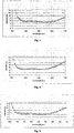
- Figures 1, 2 and 3 show the reflection spectra of the substrate respectively coated in accordance with Comparative Example 1 and Examples 2 and 3.
- a stack : glass / TiO 2 / SiO 2 : Al / TiO 2 / SiO 2 :Al is formed by magnetron sputtering on a 2.1 mm thick substrate of soda-lime type clear mineral glass.
- the deposition conditions of the different layers forming the stack are as follows.
- a first layer of titanium oxide was deposited on the substrate using a Ti metal target in a mixed atmosphere of argon and oxygen (67.6 10 -3 Pa.m 3 /s of Ar and 60.8 10 -3 Pa.m 3 /s of 02), the pressure amounted to 4.2 mbar.
- the thickness of the deposit was in the order of 10.6 nm.
- the second layer was formed using a couple of Si targets doped with 6% Al in a mixed atmosphere of argon and oxygen (135.2 10 -3 Pa.m 3 /s of Ar and 76.05 10 -3 Pa.m 3 /s of 02), the pressure amounted to 7.0 mbar.
- the electric power used supplied a rectangular amplitude-symmetric bipolar voltage to the targets.
- One period of this signal can be described as follows: +520V for 10 ⁇ sec, 0V for 10 ⁇ sec, - 520V for 10 ⁇ sec, 0V for 10 ⁇ sec.
- the thickness of the deposit was in the order of 27.9 nm.
- the third layer was deposited in the same conditions as the first.
- the thickness of the layer was in the order of 116.9 nm.
- the fourth layer was deposited in a similar manner to that of the second layer.
- the deposit thickness was in the order of 83.4 nm and the reflective index was 1.48.
- the abrasion resistance was evaluated by means of a sand abrasion test: a felt pad impregnated with an aqueous solution containing fine sand was caused to move linearly back and forth on the surface of the tested sample. After 600 runs the sample was examined and a classification given depending on the rate of abrasion of the lamination structure.
- the lamination structure described in Example 1 was given a classification of 3.
- An identical lamination structure, in which the layers of SiO 2 :Al had been deposited with an electric power supply emitting a continuous signal would only typically attain a classification of 1 to 2.
- a lamination structure glass / TiO 2 / SiO 2 :Al / TiO 2 / SiO 2 :Al / SiO 2 :Zr was formed. The first four layers were deposited in a similar manner to that of Comparative Example 1. A fifth layer of SiO 2 :Zr was formed using an Si target doped with 10% Zr in a mixed atmosphere of argon and oxygen (60.8 10 -3 Pa.m 3 /s of Ar and 84.5 10 -3 Pa.m 3 /s of O 2 ), the pressure amounted to 3.4 mbar.
- the first three layers had similar thicknesses to those of Comparative Example 1.
- the thickness of the fourth layer was 63.9 nm and the thickness of the fifth layer was 12 nm.
- Example 2 After 600 runs of the sand abrasion pad, the stack described in Example 2 was given a classification of 4.5.
- a stack glass / TiO 2 / SiO 2 :Al / TiO 2 / SiO 2 :Al / SiON was formed.
- the first four layers were deposited in a similar manner to that of Comparative Example 1.
- a fifth layer of SiON was formed using an Si target doped with 6% Al in a mixed atmosphere of argon, oxygen and nitrogen (126.75 10 -3 Pa.m 3 /s of Ar, 40.6 10 -3 Pa.m 3 /s of O 2 and 42.25 10 -3 Pa.m 3 /s of N2), the pressure amounted to 6.6 mbar.
- the first three layers had similar thicknesses to those of Comparative Example 1.
- the thickness of the fourth layer was 70.4 nm (704 ⁇ ) and the thickness of the fifth layer was 6 nm (60 ⁇ ).
- the reflection spectrum of the lamination structure described above is shown in Figure 3 and this also exhibits the typical characteristics of an anti-reflective coating with four alternating layers with high and low reflection factor.
- Example 3 After 600 runs of the sand abrasion pad, the lamination structure described in Example 3 was given a classification of 3.5.
Landscapes
- Chemical & Material Sciences (AREA)
- Physics & Mathematics (AREA)
- Engineering & Computer Science (AREA)
- General Physics & Mathematics (AREA)
- Optics & Photonics (AREA)
- Life Sciences & Earth Sciences (AREA)
- Inorganic Chemistry (AREA)
- Chemical Kinetics & Catalysis (AREA)
- General Chemical & Material Sciences (AREA)
- Geochemistry & Mineralogy (AREA)
- Materials Engineering (AREA)
- Organic Chemistry (AREA)
- Surface Treatment Of Glass (AREA)
- Laminated Bodies (AREA)
- Physical Vapour Deposition (AREA)
Claims (13)
- Substrat transparent, en particulier en verre, revêtu avec une pile de couches déposées au moyen d'un procédé de dépôt sous vide, cette structure de stratification étant constituée successivement de :i) une couche ayant un indice de réfraction élevéii) une couche ayant un indice de réfraction faibleiii) une deuxième couche ayant un indice de réfraction élevéiv) une deuxième couche ayant un indice de réfraction faible composée de deux sous-couches de compositions différentes, toutes deux composées d'un oxyde de silicium dopé avec un élément métallique,l'épaisseur de couche optique iii) étant supérieure à λο/4 où λο est la longueur d'onde centrale du revêtement antireflet,
les couches i) et iii) ayant un indice supérieur à 2,1, et
les couches ii) et iv) ayant un indice dans la plage comprise entre 1,4 et 1,8
dans lequel les couches ii) et iv) sont déposées par pulvérisation magnétiquement activée au moyen d'une cathode alimentée par un signal bipolaire de type sinusoïdal ou rectangulaire. - Substrat selon la revendication précédente, caractérisé en ce que les couches i) et iii) ont un indice supérieur à 2,3.
- Substrat selon l'une quelconque des revendications précédentes, caractérisé en ce que les couches i) et iii) comprennent un matériau diélectrique choisi parmi les oxydes de titane, de zirconium, de cérium, de niobium ou des oxydes mixtes contenant au moins un de ces éléments.
- Substrat selon l'une quelconque des revendications précédentes, caractérisé en ce que les couches ii) et iv) ont un indice dans la plage comprise entre 1,45 et 1,7, et plus préférablement dans la plage comprise entre 1,45 et 1,6.
- Substrat selon l'une quelconque des revendications précédentes, caractérisé en ce que les couches ii) et iv) comprennent un matériau diélectrique comprenant de l'oxyde de silicium, de préférence dopé avec un élément choisi parmi l'aluminium et le zirconium.
- Substrat selon l'une quelconque des revendications précédentes, caractérisé en ce que les épaisseurs géométriques de chacune des couches sont dans la plage comprise :entre 7 et 17 nm, de préférence entre 8,5 et 15 nm, pour la couche i),entre 22 et 45 nm, de préférence entre 26 et 41 nm, pour la couche ii),entre 85 et 150 nm, de préférence entre 105 et 140 nm, pour la couche iii),entre 65 et 110 nm, de préférence entre 80 et 97 nm, pour la couche iv).
- Substrat selon l'une quelconque des revendications précédentes, caractérisé en ce que les épaisseurs optiques de chacune des couches sont dans la plage comprise :entre 15 et 42 nm, de préférence entre 20 et 36 nm, pour la couche i),entre 32 et 67 nm, de préférence entre 38,5 et 60 nm, pour la couche ii),entre 214 et 380 nm, de préférence entre 252 et 350 nm, pour la couche iii),entre 100 et 157 nm, de préférence entre 118 et 143 nm, pour la couche iv).
- Substrat selon la revendication 1, caractérisé en ce que la première sous-couche de la couche iv) est composée d'oxyde de silicium, dopé avec un élément métallique de préférence choisi parmi l'aluminium et le zirconium.
- Substrat selon l'une quelconque des revendications 7 à 8, caractérisé en ce que la deuxième sous-couche de la couche iv) comprend un oxynitrure de silicium ou un oxyde de silicium dopé, en particulier, avec du zirconium.
- Procédé de production d'un substrat transparent revêtu avec une pile antireflet comprenant le dépôt au moyen d'un procédé de dépôt de type sous vide par pulvérisation magnétron de :i) une couche de matériaux diélectriques ayant un indice de réfraction élevé,ii) une couche de matériaux diélectriques ayant un indice de réfraction faibleiii) une couche de matériau diélectrique ayant un indice de réfraction élevéiv) une couche de matériaux diélectriques ayant un indice de réfraction faible,les couches i) et iii) ayant un indice supérieur à 2,1, et
les couches ii) et iv) ayant un indice dans la plage comprise entre 1,4 et 1,8,
les couches ii) et iv) étant déposées par pulvérisation magnétiquement activée au moyen d'une cathode alimentée par un signal bipolaire sinusoïdal ou rectangulaire. - Procédé selon la revendication 10, caractérisé en ce que les couches ii) et/ou iv) sont déposées au moyen de cathodes à double cible.
- Procédé selon l'une quelconque des revendications 10 à 11 pour la production d'un substrat selon l'une quelconque des revendications 1 à 9.
- Utilisation d'un substrat selon l'une quelconque des revendications 1 à 9 en tant que vitrage antireflet pour des applications architecturales.
Priority Applications (2)
| Application Number | Priority Date | Filing Date | Title |
|---|---|---|---|
| PL04766863T PL1765739T3 (pl) | 2003-09-29 | 2004-09-29 | Przezroczyste podłoże zawierające antyrefleksyjny stos warstw |
| EP04766863.7A EP1765739B1 (fr) | 2003-09-29 | 2004-09-29 | Substrat transparent comprenant un empilement antireflechissant de couches |
Applications Claiming Priority (3)
| Application Number | Priority Date | Filing Date | Title |
|---|---|---|---|
| EP03103596 | 2003-09-29 | ||
| PCT/EP2004/052351 WO2005030663A1 (fr) | 2003-09-29 | 2004-09-29 | Substrat transparent comprenant un empilement antireflechissant de couches |
| EP04766863.7A EP1765739B1 (fr) | 2003-09-29 | 2004-09-29 | Substrat transparent comprenant un empilement antireflechissant de couches |
Publications (2)
| Publication Number | Publication Date |
|---|---|
| EP1765739A1 EP1765739A1 (fr) | 2007-03-28 |
| EP1765739B1 true EP1765739B1 (fr) | 2019-08-14 |
Family
ID=34384667
Family Applications (1)
| Application Number | Title | Priority Date | Filing Date |
|---|---|---|---|
| EP04766863.7A Expired - Lifetime EP1765739B1 (fr) | 2003-09-29 | 2004-09-29 | Substrat transparent comprenant un empilement antireflechissant de couches |
Country Status (5)
| Country | Link |
|---|---|
| EP (1) | EP1765739B1 (fr) |
| ES (1) | ES2745429T3 (fr) |
| HU (1) | HUE045187T2 (fr) |
| PL (1) | PL1765739T3 (fr) |
| WO (1) | WO2005030663A1 (fr) |
Families Citing this family (5)
| Publication number | Priority date | Publication date | Assignee | Title |
|---|---|---|---|---|
| TW200718790A (en) * | 2005-11-04 | 2007-05-16 | Applied Vacuum Coating Technologies Co Ltd | Low temperature sputtering anti-reflection layer structure on sheet and manufacturing method thereof |
| FR3002767B1 (fr) * | 2013-03-01 | 2015-02-27 | Saint Gobain | Dispositif de visualisation pour vitrages transparents |
| CN105814003B (zh) * | 2013-12-16 | 2018-11-30 | Agc株式会社 | 带防反射膜玻璃及其制造方法 |
| WO2016167127A1 (fr) * | 2015-04-14 | 2016-10-20 | 旭硝子株式会社 | Verre doté d'un film antireflet |
| CN120693547A (zh) * | 2023-02-14 | 2025-09-23 | 维特罗平板玻璃有限责任公司 | 半透明镜子 |
Citations (1)
| Publication number | Priority date | Publication date | Assignee | Title |
|---|---|---|---|---|
| US5170291A (en) * | 1989-12-19 | 1992-12-08 | Leybold Aktiengesellschaft | Coating, composed of an optically effective layer system, for substrates, whereby the layer system has a high anti-reflective effect, and method for manufacturing the coating |
Family Cites Families (3)
| Publication number | Priority date | Publication date | Assignee | Title |
|---|---|---|---|---|
| JPH01273001A (ja) * | 1988-04-25 | 1989-10-31 | Olympus Optical Co Ltd | 合成樹脂製光学部品の反射防止膜 |
| JP2697000B2 (ja) * | 1988-10-11 | 1998-01-14 | 日本板硝子株式会社 | 光学膜を被覆した物品 |
| US6074730A (en) * | 1997-12-31 | 2000-06-13 | The Boc Group, Inc. | Broad-band antireflection coating having four sputtered layers |
-
2004
- 2004-09-29 WO PCT/EP2004/052351 patent/WO2005030663A1/fr not_active Ceased
- 2004-09-29 EP EP04766863.7A patent/EP1765739B1/fr not_active Expired - Lifetime
- 2004-09-29 HU HUE04766863A patent/HUE045187T2/hu unknown
- 2004-09-29 ES ES04766863T patent/ES2745429T3/es not_active Expired - Lifetime
- 2004-09-29 PL PL04766863T patent/PL1765739T3/pl unknown
Patent Citations (1)
| Publication number | Priority date | Publication date | Assignee | Title |
|---|---|---|---|---|
| US5170291A (en) * | 1989-12-19 | 1992-12-08 | Leybold Aktiengesellschaft | Coating, composed of an optically effective layer system, for substrates, whereby the layer system has a high anti-reflective effect, and method for manufacturing the coating |
Also Published As
| Publication number | Publication date |
|---|---|
| HUE045187T2 (hu) | 2019-12-30 |
| ES2745429T3 (es) | 2020-03-02 |
| PL1765739T3 (pl) | 2020-04-30 |
| EP1765739A1 (fr) | 2007-03-28 |
| WO2005030663A1 (fr) | 2005-04-07 |
Similar Documents
| Publication | Publication Date | Title |
|---|---|---|
| EP0871792B1 (fr) | Procede pour appliquer un revetement de dioxyde de titane sur un substrat | |
| US5691044A (en) | Light absorptive antireflector | |
| CN1112461C (zh) | 耐久的溅射金属氧化物镀层 | |
| KR100691168B1 (ko) | 유전 장벽층 필름 | |
| EP1781578B1 (fr) | Substrats revetus comportant une couche intermediaire | |
| EP1641722B1 (fr) | Revetements a faible emissivite resistants a la corrosion | |
| EP1194385B1 (fr) | Couches protectrices pour article revetu par pulverisation | |
| US20110293929A1 (en) | Air oxidizable scratch resistant protective layer for optical coatings | |
| US6266193B1 (en) | Anti-reflective composite | |
| EP3774683B1 (fr) | Vitre revêtue | |
| CN102649327A (zh) | 具有抗反射涂层的基板和用于制造该基板的方法 | |
| JPH05254969A (ja) | 機能性物品 | |
| WO1991002102A1 (fr) | Film base sur du dioxide de silicium et sa production | |
| EP3924313A1 (fr) | Article fonctionnel revêtu | |
| Szczyrbowski et al. | Large-scale antireflective coatings on glass produced by reactive magnetron sputtering | |
| EP1765739B1 (fr) | Substrat transparent comprenant un empilement antireflechissant de couches | |
| JP4837271B2 (ja) | 反射防止膜の形成方法 | |
| WO2011071737A2 (fr) | Structures simples de vitrage solaire à faible émissivité avec facteur de réflexion réduit dans le visible | |
| JPH05221689A (ja) | 熱線遮蔽ガラス | |
| JP2817287B2 (ja) | 透明物品 | |
| JP2001295039A (ja) | 撥水性の物品および撥水性の薄膜の被覆方法 | |
| TW202436262A (zh) | 具有光吸收器的太陽能控制玻璃 | |
| Zega | High-Rate Sputtering For Optical Purposes | |
| HK1066247B (en) | Durable sputtered metal oxide coating | |
| HK1237420B (zh) | 温度及腐蚀稳定的表面反射器 |
Legal Events
| Date | Code | Title | Description |
|---|---|---|---|
| PUAI | Public reference made under article 153(3) epc to a published international application that has entered the european phase |
Free format text: ORIGINAL CODE: 0009012 |
|
| 17P | Request for examination filed |
Effective date: 20070202 |
|
| AK | Designated contracting states |
Kind code of ref document: A1 Designated state(s): AT BE BG CH CY CZ DE DK EE ES FI FR GB GR HU IE IT LI LU MC NL PL PT RO SE SI SK TR |
|
| RAP1 | Party data changed (applicant data changed or rights of an application transferred) |
Owner name: AGC FLAT GLASS EUROPE SA |
|
| 17Q | First examination report despatched |
Effective date: 20071023 |
|
| RAP1 | Party data changed (applicant data changed or rights of an application transferred) |
Owner name: AGC GLASS EUROPE |
|
| RAP1 | Party data changed (applicant data changed or rights of an application transferred) |
Owner name: AGC GLASS EUROPE |
|
| STAA | Information on the status of an ep patent application or granted ep patent |
Free format text: STATUS: EXAMINATION IS IN PROGRESS |
|
| GRAP | Despatch of communication of intention to grant a patent |
Free format text: ORIGINAL CODE: EPIDOSNIGR1 |
|
| STAA | Information on the status of an ep patent application or granted ep patent |
Free format text: STATUS: GRANT OF PATENT IS INTENDED |
|
| INTG | Intention to grant announced |
Effective date: 20190329 |
|
| GRAS | Grant fee paid |
Free format text: ORIGINAL CODE: EPIDOSNIGR3 |
|
| GRAA | (expected) grant |
Free format text: ORIGINAL CODE: 0009210 |
|
| STAA | Information on the status of an ep patent application or granted ep patent |
Free format text: STATUS: THE PATENT HAS BEEN GRANTED |
|
| AK | Designated contracting states |
Kind code of ref document: B1 Designated state(s): AT BE BG CH CY CZ DE DK EE ES FI FR GB GR HU IE IT LI LU MC NL PL PT RO SE SI SK TR |
|
| REG | Reference to a national code |
Ref country code: GB Ref legal event code: FG4D |
|
| REG | Reference to a national code |
Ref country code: CH Ref legal event code: EP Ref country code: AT Ref legal event code: REF Ref document number: 1166813 Country of ref document: AT Kind code of ref document: T Effective date: 20190815 |
|
| REG | Reference to a national code |
Ref country code: IE Ref legal event code: FG4D |
|
| REG | Reference to a national code |
Ref country code: DE Ref legal event code: R096 Ref document number: 602004054186 Country of ref document: DE |
|
| REG | Reference to a national code |
Ref country code: RO Ref legal event code: EPE |
|
| REG | Reference to a national code |
Ref country code: NL Ref legal event code: MP Effective date: 20190814 |
|
| REG | Reference to a national code |
Ref country code: HU Ref legal event code: AG4A Ref document number: E045187 Country of ref document: HU |
|
| PG25 | Lapsed in a contracting state [announced via postgrant information from national office to epo] |
Ref country code: NL Free format text: LAPSE BECAUSE OF FAILURE TO SUBMIT A TRANSLATION OF THE DESCRIPTION OR TO PAY THE FEE WITHIN THE PRESCRIBED TIME-LIMIT Effective date: 20190814 Ref country code: PT Free format text: LAPSE BECAUSE OF FAILURE TO SUBMIT A TRANSLATION OF THE DESCRIPTION OR TO PAY THE FEE WITHIN THE PRESCRIBED TIME-LIMIT Effective date: 20191216 Ref country code: SE Free format text: LAPSE BECAUSE OF FAILURE TO SUBMIT A TRANSLATION OF THE DESCRIPTION OR TO PAY THE FEE WITHIN THE PRESCRIBED TIME-LIMIT Effective date: 20190814 Ref country code: FI Free format text: LAPSE BECAUSE OF FAILURE TO SUBMIT A TRANSLATION OF THE DESCRIPTION OR TO PAY THE FEE WITHIN THE PRESCRIBED TIME-LIMIT Effective date: 20190814 |
|
| REG | Reference to a national code |
Ref country code: AT Ref legal event code: MK05 Ref document number: 1166813 Country of ref document: AT Kind code of ref document: T Effective date: 20190814 |
|
| PG25 | Lapsed in a contracting state [announced via postgrant information from national office to epo] |
Ref country code: GR Free format text: LAPSE BECAUSE OF FAILURE TO SUBMIT A TRANSLATION OF THE DESCRIPTION OR TO PAY THE FEE WITHIN THE PRESCRIBED TIME-LIMIT Effective date: 20191115 |
|
| REG | Reference to a national code |
Ref country code: ES Ref legal event code: FG2A Ref document number: 2745429 Country of ref document: ES Kind code of ref document: T3 Effective date: 20200302 |
|
| PG25 | Lapsed in a contracting state [announced via postgrant information from national office to epo] |
Ref country code: DK Free format text: LAPSE BECAUSE OF FAILURE TO SUBMIT A TRANSLATION OF THE DESCRIPTION OR TO PAY THE FEE WITHIN THE PRESCRIBED TIME-LIMIT Effective date: 20190814 Ref country code: AT Free format text: LAPSE BECAUSE OF FAILURE TO SUBMIT A TRANSLATION OF THE DESCRIPTION OR TO PAY THE FEE WITHIN THE PRESCRIBED TIME-LIMIT Effective date: 20190814 Ref country code: EE Free format text: LAPSE BECAUSE OF FAILURE TO SUBMIT A TRANSLATION OF THE DESCRIPTION OR TO PAY THE FEE WITHIN THE PRESCRIBED TIME-LIMIT Effective date: 20190814 |
|
| PG25 | Lapsed in a contracting state [announced via postgrant information from national office to epo] |
Ref country code: MC Free format text: LAPSE BECAUSE OF FAILURE TO SUBMIT A TRANSLATION OF THE DESCRIPTION OR TO PAY THE FEE WITHIN THE PRESCRIBED TIME-LIMIT Effective date: 20190814 Ref country code: SK Free format text: LAPSE BECAUSE OF FAILURE TO SUBMIT A TRANSLATION OF THE DESCRIPTION OR TO PAY THE FEE WITHIN THE PRESCRIBED TIME-LIMIT Effective date: 20190814 |
|
| REG | Reference to a national code |
Ref country code: CH Ref legal event code: PL |
|
| REG | Reference to a national code |
Ref country code: DE Ref legal event code: R097 Ref document number: 602004054186 Country of ref document: DE |
|
| PLBE | No opposition filed within time limit |
Free format text: ORIGINAL CODE: 0009261 |
|
| STAA | Information on the status of an ep patent application or granted ep patent |
Free format text: STATUS: NO OPPOSITION FILED WITHIN TIME LIMIT |
|
| PG25 | Lapsed in a contracting state [announced via postgrant information from national office to epo] |
Ref country code: LI Free format text: LAPSE BECAUSE OF NON-PAYMENT OF DUE FEES Effective date: 20190930 Ref country code: CH Free format text: LAPSE BECAUSE OF NON-PAYMENT OF DUE FEES Effective date: 20190930 Ref country code: IE Free format text: LAPSE BECAUSE OF NON-PAYMENT OF DUE FEES Effective date: 20190929 |
|
| 26N | No opposition filed |
Effective date: 20200603 |
|
| PG25 | Lapsed in a contracting state [announced via postgrant information from national office to epo] |
Ref country code: SI Free format text: LAPSE BECAUSE OF FAILURE TO SUBMIT A TRANSLATION OF THE DESCRIPTION OR TO PAY THE FEE WITHIN THE PRESCRIBED TIME-LIMIT Effective date: 20190814 |
|
| PG25 | Lapsed in a contracting state [announced via postgrant information from national office to epo] |
Ref country code: CY Free format text: LAPSE BECAUSE OF FAILURE TO SUBMIT A TRANSLATION OF THE DESCRIPTION OR TO PAY THE FEE WITHIN THE PRESCRIBED TIME-LIMIT Effective date: 20190814 |
|
| PGFP | Annual fee paid to national office [announced via postgrant information from national office to epo] |
Ref country code: LU Payment date: 20210910 Year of fee payment: 18 Ref country code: IT Payment date: 20210811 Year of fee payment: 18 Ref country code: CZ Payment date: 20210915 Year of fee payment: 18 |
|
| PGFP | Annual fee paid to national office [announced via postgrant information from national office to epo] |
Ref country code: RO Payment date: 20210831 Year of fee payment: 18 Ref country code: HU Payment date: 20210815 Year of fee payment: 18 Ref country code: PL Payment date: 20210811 Year of fee payment: 18 Ref country code: BE Payment date: 20210817 Year of fee payment: 18 |
|
| PGFP | Annual fee paid to national office [announced via postgrant information from national office to epo] |
Ref country code: ES Payment date: 20211005 Year of fee payment: 18 |
|
| PGFP | Annual fee paid to national office [announced via postgrant information from national office to epo] |
Ref country code: TR Payment date: 20220928 Year of fee payment: 19 Ref country code: GB Payment date: 20220811 Year of fee payment: 19 Ref country code: DE Payment date: 20220809 Year of fee payment: 19 Ref country code: BG Payment date: 20220818 Year of fee payment: 19 |
|
| PGFP | Annual fee paid to national office [announced via postgrant information from national office to epo] |
Ref country code: FR Payment date: 20220808 Year of fee payment: 19 |
|
| PG25 | Lapsed in a contracting state [announced via postgrant information from national office to epo] |
Ref country code: RO Free format text: LAPSE BECAUSE OF NON-PAYMENT OF DUE FEES Effective date: 20220929 Ref country code: CZ Free format text: LAPSE BECAUSE OF NON-PAYMENT OF DUE FEES Effective date: 20220929 |
|
| REG | Reference to a national code |
Ref country code: BE Ref legal event code: MM Effective date: 20220930 |
|
| PG25 | Lapsed in a contracting state [announced via postgrant information from national office to epo] |
Ref country code: LU Free format text: LAPSE BECAUSE OF NON-PAYMENT OF DUE FEES Effective date: 20220929 |
|
| PG25 | Lapsed in a contracting state [announced via postgrant information from national office to epo] |
Ref country code: HU Free format text: LAPSE BECAUSE OF NON-PAYMENT OF DUE FEES Effective date: 20220930 |
|
| PG25 | Lapsed in a contracting state [announced via postgrant information from national office to epo] |
Ref country code: BE Free format text: LAPSE BECAUSE OF NON-PAYMENT OF DUE FEES Effective date: 20220930 |
|
| REG | Reference to a national code |
Ref country code: ES Ref legal event code: FD2A Effective date: 20231030 |
|
| PG25 | Lapsed in a contracting state [announced via postgrant information from national office to epo] |
Ref country code: IT Free format text: LAPSE BECAUSE OF NON-PAYMENT OF DUE FEES Effective date: 20220929 |
|
| PG25 | Lapsed in a contracting state [announced via postgrant information from national office to epo] |
Ref country code: ES Free format text: LAPSE BECAUSE OF NON-PAYMENT OF DUE FEES Effective date: 20220930 |
|
| PG25 | Lapsed in a contracting state [announced via postgrant information from national office to epo] |
Ref country code: ES Free format text: LAPSE BECAUSE OF NON-PAYMENT OF DUE FEES Effective date: 20220930 |
|
| REG | Reference to a national code |
Ref country code: DE Ref legal event code: R119 Ref document number: 602004054186 Country of ref document: DE |
|
| PG25 | Lapsed in a contracting state [announced via postgrant information from national office to epo] |
Ref country code: BG Free format text: LAPSE BECAUSE OF NON-PAYMENT OF DUE FEES Effective date: 20240331 |
|
| GBPC | Gb: european patent ceased through non-payment of renewal fee |
Effective date: 20230929 |
|
| PG25 | Lapsed in a contracting state [announced via postgrant information from national office to epo] |
Ref country code: PL Free format text: LAPSE BECAUSE OF NON-PAYMENT OF DUE FEES Effective date: 20220929 |
|
| PG25 | Lapsed in a contracting state [announced via postgrant information from national office to epo] |
Ref country code: GB Free format text: LAPSE BECAUSE OF NON-PAYMENT OF DUE FEES Effective date: 20230929 |
|
| PG25 | Lapsed in a contracting state [announced via postgrant information from national office to epo] |
Ref country code: GB Free format text: LAPSE BECAUSE OF NON-PAYMENT OF DUE FEES Effective date: 20230929 Ref country code: FR Free format text: LAPSE BECAUSE OF NON-PAYMENT OF DUE FEES Effective date: 20230930 Ref country code: DE Free format text: LAPSE BECAUSE OF NON-PAYMENT OF DUE FEES Effective date: 20240403 |