EP1768094A1 - Anzeigevorrichtung und ihr Ansteuerverfahren - Google Patents
Anzeigevorrichtung und ihr Ansteuerverfahren Download PDFInfo
- Publication number
- EP1768094A1 EP1768094A1 EP05108889A EP05108889A EP1768094A1 EP 1768094 A1 EP1768094 A1 EP 1768094A1 EP 05108889 A EP05108889 A EP 05108889A EP 05108889 A EP05108889 A EP 05108889A EP 1768094 A1 EP1768094 A1 EP 1768094A1
- Authority
- EP
- European Patent Office
- Prior art keywords
- pixels
- period
- during
- rows
- polarity
- Prior art date
- Legal status (The legal status is an assumption and is not a legal conclusion. Google has not performed a legal analysis and makes no representation as to the accuracy of the status listed.)
- Withdrawn
Links
- 238000000034 method Methods 0.000 title claims abstract description 32
- 239000004973 liquid crystal related substance Substances 0.000 claims description 6
- 230000001413 cellular effect Effects 0.000 claims description 2
- 239000008186 active pharmaceutical agent Substances 0.000 description 30
- 230000010287 polarization Effects 0.000 description 23
- 238000010586 diagram Methods 0.000 description 6
- 239000003990 capacitor Substances 0.000 description 2
- 230000005684 electric field Effects 0.000 description 2
- 239000011159 matrix material Substances 0.000 description 2
- 238000012986 modification Methods 0.000 description 2
- 230000004048 modification Effects 0.000 description 2
- 238000011982 device technology Methods 0.000 description 1
- 239000007788 liquid Substances 0.000 description 1
- 239000000463 material Substances 0.000 description 1
Images




Classifications
-
- G—PHYSICS
- G09—EDUCATION; CRYPTOGRAPHY; DISPLAY; ADVERTISING; SEALS
- G09G—ARRANGEMENTS OR CIRCUITS FOR CONTROL OF INDICATING DEVICES USING STATIC MEANS TO PRESENT VARIABLE INFORMATION
- G09G3/00—Control arrangements or circuits, of interest only in connection with visual indicators other than cathode-ray tubes
- G09G3/20—Control arrangements or circuits, of interest only in connection with visual indicators other than cathode-ray tubes for presentation of an assembly of a number of characters, e.g. a page, by composing the assembly by combination of individual elements arranged in a matrix no fixed position being assigned to or needed to be assigned to the individual characters or partial characters
- G09G3/34—Control arrangements or circuits, of interest only in connection with visual indicators other than cathode-ray tubes for presentation of an assembly of a number of characters, e.g. a page, by composing the assembly by combination of individual elements arranged in a matrix no fixed position being assigned to or needed to be assigned to the individual characters or partial characters by control of light from an independent source
- G09G3/36—Control arrangements or circuits, of interest only in connection with visual indicators other than cathode-ray tubes for presentation of an assembly of a number of characters, e.g. a page, by composing the assembly by combination of individual elements arranged in a matrix no fixed position being assigned to or needed to be assigned to the individual characters or partial characters by control of light from an independent source using liquid crystals
- G09G3/3611—Control of matrices with row and column drivers
- G09G3/3614—Control of polarity reversal in general
-
- G—PHYSICS
- G09—EDUCATION; CRYPTOGRAPHY; DISPLAY; ADVERTISING; SEALS
- G09G—ARRANGEMENTS OR CIRCUITS FOR CONTROL OF INDICATING DEVICES USING STATIC MEANS TO PRESENT VARIABLE INFORMATION
- G09G2310/00—Command of the display device
- G09G2310/02—Addressing, scanning or driving the display screen or processing steps related thereto
- G09G2310/0224—Details of interlacing
-
- G—PHYSICS
- G09—EDUCATION; CRYPTOGRAPHY; DISPLAY; ADVERTISING; SEALS
- G09G—ARRANGEMENTS OR CIRCUITS FOR CONTROL OF INDICATING DEVICES USING STATIC MEANS TO PRESENT VARIABLE INFORMATION
- G09G2320/00—Control of display operating conditions
- G09G2320/02—Improving the quality of display appearance
- G09G2320/0247—Flicker reduction other than flicker reduction circuits used for single beam cathode-ray tubes
-
- G—PHYSICS
- G09—EDUCATION; CRYPTOGRAPHY; DISPLAY; ADVERTISING; SEALS
- G09G—ARRANGEMENTS OR CIRCUITS FOR CONTROL OF INDICATING DEVICES USING STATIC MEANS TO PRESENT VARIABLE INFORMATION
- G09G3/00—Control arrangements or circuits, of interest only in connection with visual indicators other than cathode-ray tubes
- G09G3/20—Control arrangements or circuits, of interest only in connection with visual indicators other than cathode-ray tubes for presentation of an assembly of a number of characters, e.g. a page, by composing the assembly by combination of individual elements arranged in a matrix no fixed position being assigned to or needed to be assigned to the individual characters or partial characters
- G09G3/34—Control arrangements or circuits, of interest only in connection with visual indicators other than cathode-ray tubes for presentation of an assembly of a number of characters, e.g. a page, by composing the assembly by combination of individual elements arranged in a matrix no fixed position being assigned to or needed to be assigned to the individual characters or partial characters by control of light from an independent source
- G09G3/36—Control arrangements or circuits, of interest only in connection with visual indicators other than cathode-ray tubes for presentation of an assembly of a number of characters, e.g. a page, by composing the assembly by combination of individual elements arranged in a matrix no fixed position being assigned to or needed to be assigned to the individual characters or partial characters by control of light from an independent source using liquid crystals
- G09G3/3611—Control of matrices with row and column drivers
- G09G3/3648—Control of matrices with row and column drivers using an active matrix
Definitions
- the invention relates to driving methods for display devices, such as liquid display devices (LCDs).
- LCDs liquid display devices
- LCDs liquid crystal displays
- PDAs personal digital assistants
- portable computers portable computers
- mobile phones and the like.
- inversion driving In LCDs, liquid crystal material can degrade if an electric field is applied thereto continuously in the same direction. Thus, the direction in which the electric field is applied should be constantly changed. Namely, pixel electrode voltage (data signal) typically alternates between positive values and negative values. Such switching of electrode voltage values is referred to as inversion driving.
- inversion driving methods include dot inversion, , column inversion, line inversion, and dot column inversion.
- Fig. 1 is a schematic diagram of a part of a typical LCD panel circuit. As shown, the circuit includes data lines Dn-1, Dn and Dn+1, scan lines Gm-1, Gm and Gm+1, and corresponding display units PL.
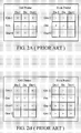
- Fig.2A is a schematic diagram of video signal polarization received by display units in the form of line inversion.
- the left side is an odd frame having data signal polarization received by display units in a panel defined by data electrodes Dn-1, Dn and Dn+1 and scan electrodes Gm-1, Gm and Gm+1
- the right side is an even frame having data signal polarization received by display units in a panel defined by the data electrodes Dn-1, Dn, Dn+1 and the scan electrodes Gm-1, Gm and Gm+1.
- Display units in the same row, such as Gm receive the same polarization data signals while display units on two adjacent rows, such as Gm-1 and Gm+1, receive opposite polarization data signals.
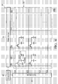
- Fig. 3A is a timing chart of the circuit shown in Fig. 2A using line inversion driving.
- the scan line Gm-1 is activated, positive polarization data signals DS on data lines Dn-1, Dn and Dn+1 are coupled to a corresponding display unit respectively.
- the polarization of the common voltage is negative.
- the scan line Gm is activated, negative polarization data signals DS on data lines Dn-1, Dn and Dn+1 are coupled to a corresponding display unit respectively.
- the polarization of the common voltage is positive.
- the scan line Gm+1 is activated, positive polarization data signals DS on lines Dn-1, Dn and Dn+1 are coupled to a corresponding display unit respectively.
- the polarization of the common voltage is negative. Namely, as each scan line is activated, the polarization of the data signals DS and the common voltage Vcom switches once. However, because the polarization switching frequency of the data signals DS equals the scan frequency of the scan lines, power consumption is high.
- Fig.2B is a schematic diagram of video signal polarization received by display units in the form of N-lines inversion.
- Fig. 3B is a timing chart of the circuit shown in Fig. 2B using an N-lines inversion driving method.
- the scan line Gm-1 is activated, and positive polarization data signals DS on lines Dn-1, Dn and Dn+1 are coupled to a corresponding display unit respectively.
- the scan line Gm is activated, and positive polarization data signals DS on lines Dn-1, Dn and Dn+1 are coupled to a corresponding display unit respectively.
- the polarization of the common voltage VCOM is negative.
- the scan line Gm+1 is activated, and negative polarization data signals DS on lines Dn-1, Dn and Dn+1 are coupled to a corresponding display unit respectively.
- the polarization of the common voltage is positive. Namely, as each two scan lines are activated in turn, the polarization of the data signals DS and common voltage VCOM switches once. This method, however, can generate flicker due to fewer polarization switches of the data signals DS and common voltage.
- An embodiment of such a driving method involves a display panel comprising pixels formed in rows.
- N th and (N+K) th rows of pixels are scanned sequentially and a signal of a first polarity is provided in sequence to the N th and (N+K) th rows of scanned pixels, during a first period of a frame period.
- (N+1) th and (N+K+1) th rows of pixels are scanned sequentially and a signal of a second polarity is provided in sequence to the (N+1) th and (N+K+1) th rows of scanned pixels, wherein N and K are both integers, N > 0, K is even and K > 1.
- An embodiment of a device comprises a display element, a gate driver and a data driver.
- the display element comprises pixels formed in rows.
- the gate driver comprises a plurality of parallel gate lines, each line coupled to a corresponding row of pixels.
- the gate driver scans a first row and a second row of pixels in sequence during a first period of a frame period, and scans a third row and fourth row of pixels during a second period of the frame period.
- the first and second rows of pixels are not adjacent nor the third and fourth rows of pixels.
- the data driver comprises a plurality of parallel data lines, each data line orthogonal to the gate lines, and coupled to a corresponding column of pixels.
- the data driver provides a signal of a first polarity in sequence to the scanned rows of pixels during the first period and a signal of a second polarity in sequence to the scanned rows of pixels during the second period.
- Fig. 4 shows an embodiment of a display device.
- the display device 400 comprises a display element 10 and a driving circuit 50.
- the display element 10 that is operatively coupled to the driving circuit 50 is an LCD element.
- the display element 10 comprises a plurality of pixels 100 arranged in a matrix.
- the display element 10 could be a plasma display element, an organic light emitting display element, or a cathode ray tube display element, for example.
- the driving circuit 50 drives the matrix of pixels 100 of an LCD device formed in X rows and Y columns, wherein X and Y are integers.
- Driving circuit 50 comprises a data driver 20, a gate driver 30 and a controller 40.
- Data driver 20 includes a plurality of parallel data lines D1 ⁇ Dy. Each data line D1 ⁇ Dy is coupled to a corresponding column of pixels 100.
- pixels 100 can each comprise a switching transistor 101 having a first terminal coupled to a corresponding data line, a control terminal coupled to a corresponding scan line, and a second terminal coupled to first terminals of a liquid crystal element Clc and a storage capacitor Cs.
- the second terminals of the liquid crystal elements Clc are coupled to a common voltage VCOM and the second terminals of the storage capacitors are coupled to a ground voltage.
- Gate driver 30 includes a plurality of parallel gate lines G1 ⁇ Gx, each orthogonal to data lines D1 ⁇ Dy. Each gate line G1 ⁇ Gx is coupled to a corresponding row of pixels 100. Controller 40 controls scanning of the gate driver 30 and signal providing of the data driver 20, and, for example, can be a timing controller.
- the gate driver 30 scans a first row and a second row of pixels in sequence and the data driver 20 provides a signal of a first polarity in sequence to the scanned (first and second) rows of pixels during a first period of a frame period.
- the gate driver 30 scans a third row and fourth row of pixels and the data driver 20 provides a signal of a second polarity in sequence to the scanned (third and fourth) rows of pixels during a second period of the frame period.
- a frame period comprises at least one first period and at least one second period, the first and second rows of pixels are not adjacent to each other and the third and fourth rows of pixels are not adjacent to each other.
- the gate driver 30 scans N th and (N+K) th rows of pixels sequentially and the data driver 20 provides a signal of a first polarity in sequence to the N th and (N+K) th rows of scanned pixels, during a first period of a frame period.
- the gate driver 30 scans (N+1) th and (N+K+1) th rows of pixels are scanned sequentially and the data driver 20 provides a signal of a second polarity in sequence to the (N+1) th and (N+K+1) th rows of scanned pixels, wherein N and K are both integers, N > 0, K is even and K > 1.
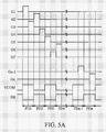
- Fig. 5A is a timing chart depicting a first embodiment of a method of operating a display device. As shown, one frame period comprises periods PD1, PD2, PD3, PD4, ..., PDn-1 and PDn. In this embodiment, N is from 1 to n and K is 2, while it is to be understood that the invention is not limited thereto.
- the gate driver 30 scans the gate lines G1 and G3 in sequence and the data driver 20 provides data signals DS of a first polarity in sequence to the scanned rows of pixels. For example, if the common voltage VCOM is kept at a positive voltage level, the first polarity is a negative voltage level with respect to the common voltage VCOM during the period PD1.
- the gate driver 30 scans the gate lines G2 and G4 in sequence and the data driver 20 provides data signals DS of a second polarity in sequence to the scanned rows of pixels. For example, if the common voltage VCOM is kept at a negative voltage level, the second polarity is a positive voltage level with respect to the common voltage VCOM during the period PD2.
- the gate driver 30 scans the gate lines G5 and G7 in sequence and the data driver 20 provides data signals DS of the first polarity in sequence to the scanned rows of pixels, and so on.
- the gate driver 30 scans the gate lines Gx-2 and Gx in sequence and the data driver 20 provides data signals DS of the second polarity in sequence to the scanned rows of pixels.
- Fig. 5B is a timing chart depicting a second embodiment of a method of operating a display device.
- the frame period comprises periods PD1, PD2, PD3, PD4, ..., PDn-1 and PDn.
- N is from 1 to n and K is 4, while it is to be understood that the invention is not limited thereto.
- the gate driver 30 scans the gate lines G1 and G5 in sequence and the data driver 20 provides data signals DS of a first polarity in sequence to the scanned rows of pixels.
- the gate driver 30 scans the gate lines G2 and G6 in sequence and the data driver 20 provides data signals DS of a second polarity in sequence to the scanned rows of pixels.
- the gate driver 30 scans the gate lines G3 and G7 in sequence and the data driver 20 provides data signals DS of the first polarity in sequence to the scanned rows of pixels.
- the gate driver 30 scans the gate lines G4 and G8 in sequence and the data driver 20 provides data signals DS of the second polarity in sequence to the scanned rows of pixels, and so on.
- the gate driver 30 scans the gate lines Gx-4 and Gx in sequence and the data driver 20 provides data signals DS of the second polarity in sequence to the scanned rows of pixels.
- the gate driver 30 scans N th , (N+K) th , and (N+2K) th rows of pixels sequentially and the data driver 20 provides a signal of a first polarity in sequence to the scanned rows of pixels, during a first period of a frame period.
- the gate driver 30 scans (N+1) th , (N+K+1) th , and (N+2K+1) th rows of pixels sequentially and the data driver 20 provides a signal of a second polarity in sequence to the scanned rows of pixels, wherein N and K are both integers, N > 0, K is even and K > 1.
- Fig. 5C is a timing chart depicting a third embodiment of a method of operating a display device.
- one frame period comprises periods PD1, PD2, PD3, PD4, ..., and PDn.
- N is from 1 to n and K is 2, while it is to be understood that the invention is not limited thereto.
- the gate driver 30 scans the gate lines G1, G3 and G5 in sequence and the data driver 20 provides data signals DS of a first polarity in sequence to the scanned rows of pixels.
- the gate driver 30 scans the gate lines G2, G4 and G6 in sequence and the data driver 20 provides data signals DS of a second polarity in sequence to the scanned rows of pixels.
- the gate driver 30 scans the gate lines G7, G9 and G11 in sequence and the data driver 20 provides data signals DS of the first polarity in sequence to the scanned rows of pixels.
- the gate driver 30 scans the gate lines G8, G10 and G12 in sequence and the data driver 20 provides data signals DS of the second polarity in sequence to the scanned rows of pixels, and so on.
- the gate driver 30 scans the gate lines Gx-4, Gx-2 and Gx in sequence and the data driver 20 provides data signals DS of the second polarity in sequence to the scanned rows of pixels.
- N can be from 1 to n and K is 4.
- the gate driver 30 scans the gate lines G1, G5 and G9 in sequence and the data driver 20 provides data signals DS of a first polarity in sequence to the scanned rows of pixels.
- the gate driver 30 scans the gate lines G2, G6 and G10 in sequence and the data driver 20 provides data signals DS of a second polarity in sequence to the scanned rows of pixels.
- the gate driver 30 scans the gate lines G3, G7 and G11 in sequence and the data driver 20 provides data signals DS of the first polarity in sequence to the scanned rows of pixels.
- the gate driver 30 scans the gate lines G4, G8 and G12 in sequence and the data driver 20 provides data signals DS of the second polarity in sequence to the scanned rows of pixels and so on.
- Fig. 5D is a timing chart depicting a fourth embodiment of a method of operating a display device. As shown, one frame period comprises periods PD1 and PD2.
- the gate driver 30 scans the odd-numbered gate lines G1, G3, ..., Gx-1 in sequence and the data driver 20 provides data signals DS of a first polarity in sequence to the scanned rows of pixels. For example, if the common voltage VCOM is kept at a positive voltage level, the first polarity is a negative voltage level with respect to the common voltage VCOM during the period PD1.
- the gate driver 30 scans the even-numbered gate lines G2, G4, ..., Gx in sequence and the data driver 20 provides data signals DS of a second polarity in sequence to the scanned rows of pixels. For example, if the common voltage VCOM is kept at a negative voltage level, the second polarity is a positive voltage level with respect to the common voltage VCOM during the period PD2.
- Fig. 6 schematically shows an embodiment of an electronic device 500 employing an embodiment of a display device.
- the display device can be a liquid crystal display system, an organic light-emitting diode (OLED) display system, or a field emission display (FED) system, although it is to be understood that the invention is not limited thereto.
- the electronic device 500 may be a portable device such as a PDA, notebook computer, tablet computer, cellular phone, or a display monitor device, etc.
- the electronic device 500 includes a housing 510, a display device such as the display device shown in Fig. 4, and a DC/DC converter 520., Further, the DC/DC converter 520 is operatively coupled to the display device and provides an output voltage powering the display device to display images.
Landscapes
- Engineering & Computer Science (AREA)
- Chemical & Material Sciences (AREA)
- Crystallography & Structural Chemistry (AREA)
- Physics & Mathematics (AREA)
- Computer Hardware Design (AREA)
- General Physics & Mathematics (AREA)
- Theoretical Computer Science (AREA)
- Control Of Indicators Other Than Cathode Ray Tubes (AREA)
Priority Applications (1)
| Application Number | Priority Date | Filing Date | Title |
|---|---|---|---|
| EP05108889A EP1768094A1 (de) | 2005-09-26 | 2005-09-26 | Anzeigevorrichtung und ihr Ansteuerverfahren |
Applications Claiming Priority (1)
| Application Number | Priority Date | Filing Date | Title |
|---|---|---|---|
| EP05108889A EP1768094A1 (de) | 2005-09-26 | 2005-09-26 | Anzeigevorrichtung und ihr Ansteuerverfahren |
Publications (1)
| Publication Number | Publication Date |
|---|---|
| EP1768094A1 true EP1768094A1 (de) | 2007-03-28 |
Family
ID=35520717
Family Applications (1)
| Application Number | Title | Priority Date | Filing Date |
|---|---|---|---|
| EP05108889A Withdrawn EP1768094A1 (de) | 2005-09-26 | 2005-09-26 | Anzeigevorrichtung und ihr Ansteuerverfahren |
Country Status (1)
| Country | Link |
|---|---|
| EP (1) | EP1768094A1 (de) |
Citations (3)
| Publication number | Priority date | Publication date | Assignee | Title |
|---|---|---|---|---|
| EP0350934A2 (de) * | 1988-07-14 | 1990-01-17 | Canon Kabushiki Kaisha | Flüssigkristallanzeigegerät |
| US5526015A (en) * | 1988-08-17 | 1996-06-11 | Canon Kabushiki Kaisha | Display apparatus having a display region and a non-display region |
| US20040183768A1 (en) * | 2003-03-20 | 2004-09-23 | Asahi Yamato | Liquid crystal display device and method for driving the same |
-
2005
- 2005-09-26 EP EP05108889A patent/EP1768094A1/de not_active Withdrawn
Patent Citations (3)
| Publication number | Priority date | Publication date | Assignee | Title |
|---|---|---|---|---|
| EP0350934A2 (de) * | 1988-07-14 | 1990-01-17 | Canon Kabushiki Kaisha | Flüssigkristallanzeigegerät |
| US5526015A (en) * | 1988-08-17 | 1996-06-11 | Canon Kabushiki Kaisha | Display apparatus having a display region and a non-display region |
| US20040183768A1 (en) * | 2003-03-20 | 2004-09-23 | Asahi Yamato | Liquid crystal display device and method for driving the same |
Similar Documents
| Publication | Publication Date | Title |
|---|---|---|
| US20070063952A1 (en) | Driving methods and devices using the same | |
| CN107665692B (zh) | 液晶显示器像素驱动电路及像素驱动方法 | |
| CN100533534C (zh) | 扫描驱动器、具有该扫描驱动器的显示设备及其驱动方法 | |
| US8416172B2 (en) | Liquid crystal display and driving method thereof | |
| US8242997B2 (en) | Liquid crystal display panel and liquid crystal display device having the same | |
| US7586358B2 (en) | Level shifter and driving method | |
| US7369187B2 (en) | Liquid crystal display device and method of driving the same | |
| EP2360671A1 (de) | Flüssigkristallanzeige und Ansteuerverfahren dafür | |
| US8106871B2 (en) | Liquid crystal display and driving method thereof | |
| US20080136801A1 (en) | Liquid crystal display and driving method thereof | |
| US20080024408A1 (en) | Systems for displaying images and driving method thereof | |
| CN1487493A (zh) | 包括主-从结构数据驱动器的液晶显示器及其驱动方法 | |
| US8373685B2 (en) | Display systems | |
| KR102050317B1 (ko) | 게이트 구동회로 및 이를 포함하는 액정표시장치 | |
| US7605790B2 (en) | Liquid crystal display device capable of reducing power consumption by charge sharing | |
| US9805673B2 (en) | Method of driving a display panel and display device performing the same | |
| US7893910B2 (en) | Method for driving liquid crystal display via circularly reversing polarities of pixels thereof | |
| CN101359109A (zh) | 像素、显示面板及其驱动方法 | |
| US20110205213A1 (en) | Liquid crystal display device | |
| US9230499B2 (en) | Source driving apparatus with power saving mechanism and flat panel display using the same | |
| US8542174B2 (en) | Display panel and driving method thereof | |
| EP1768094A1 (de) | Anzeigevorrichtung und ihr Ansteuerverfahren | |
| US20120068991A1 (en) | Active matrix display devices and electronic apparatuses using the same | |
| US7796125B2 (en) | Voltage supply circuit, power supply circuit, display driver, electro-optic device, and electronic apparatus | |
| US20070171178A1 (en) | Active matrix display device |
Legal Events
| Date | Code | Title | Description |
|---|---|---|---|
| PUAI | Public reference made under article 153(3) epc to a published international application that has entered the european phase |
Free format text: ORIGINAL CODE: 0009012 |
|
| AK | Designated contracting states |
Kind code of ref document: A1 Designated state(s): AT BE BG CH CY CZ DE DK EE ES FI FR GB GR HU IE IS IT LI LT LU LV MC NL PL PT RO SE SI SK TR |
|
| AX | Request for extension of the european patent |
Extension state: AL BA HR MK YU |
|
| 17P | Request for examination filed |
Effective date: 20070911 |
|
| AKX | Designation fees paid |
Designated state(s): AT BE BG CH CY CZ DE DK EE ES FI FR GB GR HU IE IS IT LI LT LU LV MC NL PL PT RO SE SI SK TR |
|
| 17Q | First examination report despatched |
Effective date: 20071128 |
|
| STAA | Information on the status of an ep patent application or granted ep patent |
Free format text: STATUS: THE APPLICATION IS DEEMED TO BE WITHDRAWN |
|
| 18D | Application deemed to be withdrawn |
Effective date: 20080409 |