EP1770057A2 - Procédé pour réaliser un dispositif microélectromécanique ayant un diaphragme - Google Patents
Procédé pour réaliser un dispositif microélectromécanique ayant un diaphragme Download PDFInfo
- Publication number
- EP1770057A2 EP1770057A2 EP06076693A EP06076693A EP1770057A2 EP 1770057 A2 EP1770057 A2 EP 1770057A2 EP 06076693 A EP06076693 A EP 06076693A EP 06076693 A EP06076693 A EP 06076693A EP 1770057 A2 EP1770057 A2 EP 1770057A2
- Authority
- EP
- European Patent Office
- Prior art keywords
- wafer
- diaphragm
- cavity
- active
- support
- Prior art date
- Legal status (The legal status is an assumption and is not a legal conclusion. Google has not performed a legal analysis and makes no representation as to the accuracy of the status listed.)
- Withdrawn
Links
Images


Classifications
-
- B—PERFORMING OPERATIONS; TRANSPORTING
- B81—MICROSTRUCTURAL TECHNOLOGY
- B81C—PROCESSES OR APPARATUS SPECIALLY ADAPTED FOR THE MANUFACTURE OR TREATMENT OF MICROSTRUCTURAL DEVICES OR SYSTEMS
- B81C1/00—Manufacture or treatment of devices or systems in or on a substrate
- B81C1/00642—Manufacture or treatment of devices or systems in or on a substrate for improving the physical properties of a device
- B81C1/0065—Mechanical properties
- B81C1/00666—Treatments for controlling internal stress or strain in MEMS structures
-
- B—PERFORMING OPERATIONS; TRANSPORTING
- B81—MICROSTRUCTURAL TECHNOLOGY
- B81C—PROCESSES OR APPARATUS SPECIALLY ADAPTED FOR THE MANUFACTURE OR TREATMENT OF MICROSTRUCTURAL DEVICES OR SYSTEMS
- B81C1/00—Manufacture or treatment of devices or systems in or on a substrate
- B81C1/00015—Manufacture or treatment of devices or systems in or on a substrate for manufacturing microsystems
- B81C1/00222—Integrating an electronic processing unit with a micromechanical structure
- B81C1/00246—Monolithic integration, i.e. micromechanical structure and electronic processing unit are integrated on the same substrate
-
- B—PERFORMING OPERATIONS; TRANSPORTING
- B81—MICROSTRUCTURAL TECHNOLOGY
- B81B—MICROSTRUCTURAL DEVICES OR SYSTEMS, e.g. MICROMECHANICAL DEVICES
- B81B2203/00—Basic microelectromechanical structures
- B81B2203/01—Suspended structures, i.e. structures allowing a movement
- B81B2203/0127—Diaphragms, i.e. structures separating two media that can control the passage from one medium to another; Membranes, i.e. diaphragms with filtering function
-
- B—PERFORMING OPERATIONS; TRANSPORTING
- B81—MICROSTRUCTURAL TECHNOLOGY
- B81C—PROCESSES OR APPARATUS SPECIALLY ADAPTED FOR THE MANUFACTURE OR TREATMENT OF MICROSTRUCTURAL DEVICES OR SYSTEMS
- B81C2201/00—Manufacture or treatment of microstructural devices or systems
- B81C2201/01—Manufacture or treatment of microstructural devices or systems in or on a substrate
- B81C2201/0174—Manufacture or treatment of microstructural devices or systems in or on a substrate for making multi-layered devices, film deposition or growing
- B81C2201/0191—Transfer of a layer from a carrier wafer to a device wafer
-
- B—PERFORMING OPERATIONS; TRANSPORTING
- B81—MICROSTRUCTURAL TECHNOLOGY
- B81C—PROCESSES OR APPARATUS SPECIALLY ADAPTED FOR THE MANUFACTURE OR TREATMENT OF MICROSTRUCTURAL DEVICES OR SYSTEMS
- B81C2203/00—Forming microstructural systems
- B81C2203/07—Integrating an electronic processing unit with a micromechanical structure
- B81C2203/0707—Monolithic integration, i.e. the electronic processing unit is formed on or in the same substrate as the micromechanical structure
- B81C2203/0728—Pre-CMOS, i.e. forming the micromechanical structure before the CMOS circuit
Definitions
- the present invention is generally directed to a micro-electro-mechanical (MEM) device and, more specifically, to a technique for manufacturing a MEM device.
- MEM micro-electro-mechanical
- MEM micro-electro-mechanical
- SOI silicon-on-insulator
- MEM single crystal silicon diaphragm
- MEM devices with a buried cavity process it is generally desirable to manufacture MEM devices with a buried cavity process as the size of such devices are reduced (which lowers cost), as compared to devices made through bulk etch techniques which rely on a tapered etch from the back of the handle wafer to form the diaphragm.
- MEM devices incorporating buried cavities and including moving structures that are formed with a dry deep reactive ion etch (DRIE) process do not exhibit process induced stiction problems.
- DRIE deep reactive ion etch
- MEM devices made by buried cavity techniques are, in general, temperature limited as the diaphragm may plastically deform during processing if a process temperature is too high. In general, the temperature at which a diaphragm deforms is low enough that the buried cavity technique is incompatible with most complementary metal-oxide semiconductor (CMOS) processes.
- CMOS complementary metal-oxide semiconductor
- Plastic deformation of silicon occurs when the stress in the silicon exceeds the flow stress of the silicon. In general, this occurs in buried cavity MEM processes when thin diaphragms are created and stress, induced by differential pressure across the cavity or by thin films, exceeds the flow stress limit, which is a function of temperature for silicon. While this phenomena has been utilized by designers to purposely plastically deform membranes of MEM devices that function as switches, plastic deformation is undesirable in other applications. Typically, for most applications, the membrane thickness and cavity size for a buried cavity MEM device is such that the membrane generally cannot tolerate temperatures above 800°C without experiencing plastic deformation.
- CMOS complementary metal-oxide semiconductor
- One embodiment of the present invention is directed to a technique for manufacturing a micro-electro-mechanical (MEM) device that includes a number of steps. Initially a first wafer is provided. Next, a portion of the first wafer is removed to provide a cavity including a plurality of spaced support pedestals within the cavity. Then, at least a portion of a second wafer is bonded to the first wafer. A portion of the second wafer provides a diaphragm over the cavity and the support pedestals support the diaphragm during processing. According to another aspect, the second wafer is etched to release the diaphragm from the support pedestals.
- the first wafer may be a handle wafer and the second wafer may be an active wafer, or vice versa.
- the handle and active wafers may also be silicon wafers. According to a different aspect, the pedestals are not bonded to the diaphragm.
- a process for manufacturing a MEM device includes providing a handle wafer. Next, a bonding layer is formed on a first surface of the handle wafer. Then, a portion of the bonding layer is removed to provide a cavity including a plurality of spaced support pedestals within the cavity. Next, an active wafer is bonded to at least a portion of the bonding layer. A portion of the active wafer provides a diaphragm over the cavity and support pedestals support the diaphragm during processing. The active wafer may then be etched to release the diaphragm from the support pedestals, if the pedestals are bonded to the diaphragm. This etch step may also release at least a portion of the diaphragm adjacent a sidewall of the cavity to provide a movable diaphragm.
- the handle and active wafers are silicon wafers.
- the bonding layer is made of silicon, an oxide or a nitride.
- the support pedestals support the diaphragm during processing to prevent plastic deformation of the diaphragm.
- the active wafer is thinned to provide a desired thickness for the diaphragm.
- the step of etching the active wafer to release the diaphragm from the support pedestals further comprises the step of etching at least a portion of the diaphragm adjacent a sidewall of the cavity to allow the diaphragm to move.
- a technique is disclosed herein that provides a micro-electro-mechanical (MEM) device whose moveable structure (i.e., diaphragm or membrane) is supported during processing to eliminate temperature limitations.
- MEM micro-electro-mechanical
- the stress in the silicon diaphragm is reduced. It should be appreciated that the distance between the pedestals determines the maximum stress that the silicon experiences at temperature.
- an etch may be performed around the pedestals at the end of the process to free the structures or the pedestals may be recessed so that an etch is not required to free the structures.
- CMOS complementary metal-oxide semiconductor
- the pedestals can be made of any material compatible with the processes that the MEM devices undergo.
- the bonding material may include silicon, oxides, nitrides and other semiconductor films.
- the buried cavity MEM process is initiated by forming a bonding layer 104 on a handle layer 102.
- the bonding layer may be dispensed with and two wafers may be directly bonded to each other.
- the bonding layer 104 is patterned and a cavity 105 is etched into the bonding layer 104.
- the cavity may be formed in either of the wafers.
- An active wafer 106 is then bonded to at least a portion of the bonding layer 104.
- the active wafer 106 may be thinned to a desired diaphragm thickness, which is application dependent.
- a diaphragm 110 is then released through an etch process (e.g., a deep reactive ion etch (DRIE) or other silicon etch technique), which forms trenches 108.
- etch process e.g., a deep reactive ion etch (DRIE) or other silicon etch technique
- DRIE deep reactive ion etch
- the prior art process which is described above, has temperature limits, above which plastic deformation of the diaphragm 110 can occur. As such, the MEM device of FIG. 1 is incompatible with most CMOS processes.
- manufacturing of a MEM device is initiated by forming a bonding layer 204 on a handle wafer 202, which may be, for example, a silicon wafer.
- a cavity 205 including a plurality of spaced support pedestals 204A, is then formed in the bonding layer 204.
- two wafers may be directly bonded and a cavity and support pedestals may be formed in either of the two wafers.
- An active wafer 206 is then bonded to the bonding layer 204 to provide the buried cavity 205.
- the active wafer 206 is thinned to a desired thickness.
- the active wafer 206 may be thinned prior to bonding to the bonding layer 204.
- Trenches 208 are then etched in the active wafer 206 along a sidewall of the cavity 205 to define and release at least a portion of a diaphragm 210 adjacent a sidewall of the cavity 205.
- holes 208B are etched in the active wafer 206 to release the diaphragm 210 from the support pedestals 204A, if the support pedestals 204A are not recessed.
- FIG. 2A depicts top views of another MEM device during various process handling steps.
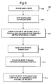
- a process 300 for manufacturing a MEM device is depicted.
- a handle wafer e.g., a silicon or glass wafer
- a bonding layer is formed on the handle wafer.
- the bonding layer may be, for example, made of silicon, an oxide, a nitride or another film.
- step 306 a portion of the bonding layer is removed to provide a cavity including support pedestals.
- step 308 the active wafer is bonded to the bonding layer.
- step 310 assuming the support pedestals are not recessed, the active wafer is etched to release the diaphragm from the support pedestals.
- step 312 if desired, the active wafer is etched to release at least a portion of the diaphragm adjacent a sidewall of the cavity.
- steps 310 and 312 may be performed in a single step. That is, the diaphragm may be released from the support pedestals and the trenches may be etched to release the diaphragm in a single step.
- a process 400 for manufacturing a MEM device using two wafers and no bonding layer is depicted.
- a first wafer e.g., a silicon or glass handle wafer
- step 404 a portion of the first wafer is removed to provide a cavity including support pedestals.
- step 406 a second wafer, e.g., an active silicon wafer is bonded to the first wafer to provide a diaphragm.
- step 408 the second wafer is thinned.
- step 408 may be deleted if the second wafer is already a desired thickness.
- step 410 the second wafer is etched to release the diaphragm from the support pedestals.
- step 410 may be deleted.
- step 412 if desired, the second wafer is etched to release at least a portion of the diaphragm adjacent a sidewall of the cavity.
- steps 410 and 412 may be performed in a single step. That is, the diaphragm may be released from the support pedestals and the trenches may be etched to release the diaphragm in a single step.
- MEM micro-electro-mechanical
Landscapes
- Engineering & Computer Science (AREA)
- Manufacturing & Machinery (AREA)
- Microelectronics & Electronic Packaging (AREA)
- Mechanical Engineering (AREA)
- Micromachines (AREA)
Applications Claiming Priority (1)
| Application Number | Priority Date | Filing Date | Title |
|---|---|---|---|
| US11/238,855 US7534641B2 (en) | 2005-09-29 | 2005-09-29 | Method for manufacturing a micro-electro-mechanical device |
Publications (2)
| Publication Number | Publication Date |
|---|---|
| EP1770057A2 true EP1770057A2 (fr) | 2007-04-04 |
| EP1770057A3 EP1770057A3 (fr) | 2008-07-16 |
Family
ID=37562516
Family Applications (1)
| Application Number | Title | Priority Date | Filing Date |
|---|---|---|---|
| EP06076693A Withdrawn EP1770057A3 (fr) | 2005-09-29 | 2006-09-07 | Procédé pour réaliser un dispositif microélectromécanique ayant un diaphragme |
Country Status (2)
| Country | Link |
|---|---|
| US (1) | US7534641B2 (fr) |
| EP (1) | EP1770057A3 (fr) |
Families Citing this family (1)
| Publication number | Priority date | Publication date | Assignee | Title |
|---|---|---|---|---|
| US9269603B2 (en) * | 2013-05-09 | 2016-02-23 | Globalfoundries Inc. | Temporary liquid thermal interface material for surface tension adhesion and thermal control |
Family Cites Families (10)
| Publication number | Priority date | Publication date | Assignee | Title |
|---|---|---|---|---|
| DE19509868A1 (de) * | 1995-03-17 | 1996-09-19 | Siemens Ag | Mikromechanisches Halbleiterbauelement |
| US5706565A (en) | 1996-09-03 | 1998-01-13 | Delco Electronics Corporation | Method for making an all-silicon capacitive pressure sensor |
| US5831162A (en) | 1997-01-21 | 1998-11-03 | Delco Electronics Corporation | Silicon micromachined motion sensor and method of making |
| US6191007B1 (en) * | 1997-04-28 | 2001-02-20 | Denso Corporation | Method for manufacturing a semiconductor substrate |
| US6211558B1 (en) * | 1997-07-18 | 2001-04-03 | Kavlico Corporation | Surface micro-machined sensor with pedestal |
| US6180428B1 (en) * | 1997-12-12 | 2001-01-30 | Xerox Corporation | Monolithic scanning light emitting devices using micromachining |
| JP3489551B2 (ja) | 2000-09-08 | 2004-01-19 | 株式会社村田製作所 | 真空容器の製造方法 |
| US20020132490A1 (en) * | 2001-03-16 | 2002-09-19 | Lieyi Sheng | Microstructure having a membrane and a wedge beneath and methods for manufacture of same |
| US6713367B2 (en) * | 2001-08-28 | 2004-03-30 | The Board Of Trustees Of The Leland Stanford Junior University | Self-aligned vertical combdrive actuator and method of fabrication |
| US6829814B1 (en) | 2002-08-29 | 2004-12-14 | Delphi Technologies, Inc. | Process of making an all-silicon microphone |
-
2005
- 2005-09-29 US US11/238,855 patent/US7534641B2/en not_active Expired - Fee Related
-
2006
- 2006-09-07 EP EP06076693A patent/EP1770057A3/fr not_active Withdrawn
Also Published As
| Publication number | Publication date |
|---|---|
| US7534641B2 (en) | 2009-05-19 |
| EP1770057A3 (fr) | 2008-07-16 |
| US20070072331A1 (en) | 2007-03-29 |
Similar Documents
| Publication | Publication Date | Title |
|---|---|---|
| KR100421217B1 (ko) | 점착 방지 미세 구조물 제조 방법 | |
| US9458009B2 (en) | Semiconductor devices and methods of forming thereof | |
| US6743654B2 (en) | Method of fabricating pressure sensor monolithically integrated | |
| US7083997B2 (en) | Bonded wafer optical MEMS process | |
| JP4431502B2 (ja) | エピタキシによって半導体デバイスを形成する方法 | |
| US7153716B2 (en) | Method of manufacturing a micro-electrical-mechanical system | |
| US8590389B2 (en) | MEMS pressure sensor device and manufacturing method thereof | |
| US8685776B2 (en) | Wafer level packaged MEMS device | |
| US20150276533A1 (en) | Low Pressure Sensor and Flow Sensor | |
| US7214324B2 (en) | Technique for manufacturing micro-electro mechanical structures | |
| US10112827B2 (en) | Process for producing an electromechanical device | |
| US9938140B2 (en) | MEMS device and method of manufacturing a MEMS device | |
| EP3095754B1 (fr) | Capteur à basse pression et capteur d'écoulement | |
| EP3150548B1 (fr) | Procédé basé sur mems destiné à la fabrication de capteur | |
| US20060278942A1 (en) | Antistiction MEMS substrate and method of manufacture | |
| US12234144B2 (en) | Method for sealing cavities using membranes | |
| CN111630673B (zh) | 用于制造包括多个微机械元件的器件的制造方法 | |
| US7534641B2 (en) | Method for manufacturing a micro-electro-mechanical device | |
| CN108341395A (zh) | 一种mems器件的制作方法 | |
| KR20020016117A (ko) | Mems 공정을 이용한 마이크로폰 제작방법 | |
| US9505612B2 (en) | Method for thin film encapsulation (TFE) of a microelectromechanical system (MEMS) device and the MEMS device encapsulated thereof | |
| KR100817813B1 (ko) | 실리콘 기판 상에 상이한 수직 단차를 갖는 미세구조물의제조 방법 | |
| US20080032501A1 (en) | Silicon on metal for mems devices | |
| US7179668B2 (en) | Technique for manufacturing silicon structures | |
| CN112875642B (zh) | Mems器件及其制造方法 |
Legal Events
| Date | Code | Title | Description |
|---|---|---|---|
| PUAI | Public reference made under article 153(3) epc to a published international application that has entered the european phase |
Free format text: ORIGINAL CODE: 0009012 |
|
| AK | Designated contracting states |
Kind code of ref document: A2 Designated state(s): AT BE BG CH CY CZ DE DK EE ES FI FR GB GR HU IE IS IT LI LT LU LV MC NL PL PT RO SE SI SK TR |
|
| AX | Request for extension of the european patent |
Extension state: AL BA HR MK YU |
|
| PUAL | Search report despatched |
Free format text: ORIGINAL CODE: 0009013 |
|
| AK | Designated contracting states |
Kind code of ref document: A3 Designated state(s): AT BE BG CH CY CZ DE DK EE ES FI FR GB GR HU IE IS IT LI LT LU LV MC NL PL PT RO SE SI SK TR |
|
| AX | Request for extension of the european patent |
Extension state: AL BA HR MK RS |
|
| 17P | Request for examination filed |
Effective date: 20090116 |
|
| AKX | Designation fees paid |
Designated state(s): AT BE BG CH CY CZ DE DK EE ES FI FR GB GR HU IE IS IT LI LT LU LV MC NL PL PT RO SE SI SK TR |
|
| 17Q | First examination report despatched |
Effective date: 20090225 |
|
| STAA | Information on the status of an ep patent application or granted ep patent |
Free format text: STATUS: THE APPLICATION IS DEEMED TO BE WITHDRAWN |
|
| 18D | Application deemed to be withdrawn |
Effective date: 20090908 |