EP1770565A1 - Intégration automatique de circuits FPGA sur une carte imprimée - Google Patents
Intégration automatique de circuits FPGA sur une carte imprimée Download PDFInfo
- Publication number
- EP1770565A1 EP1770565A1 EP05109042A EP05109042A EP1770565A1 EP 1770565 A1 EP1770565 A1 EP 1770565A1 EP 05109042 A EP05109042 A EP 05109042A EP 05109042 A EP05109042 A EP 05109042A EP 1770565 A1 EP1770565 A1 EP 1770565A1
- Authority
- EP
- European Patent Office
- Prior art keywords
- extensions
- electronic circuit
- database
- fpga
- extension part
- Prior art date
- Legal status (The legal status is an assumption and is not a legal conclusion. Google has not performed a legal analysis and makes no representation as to the accuracy of the status listed.)
- Withdrawn
Links
Images
Classifications
-
- G—PHYSICS
- G06—COMPUTING OR CALCULATING; COUNTING
- G06F—ELECTRIC DIGITAL DATA PROCESSING
- G06F30/00—Computer-aided design [CAD]
- G06F30/30—Circuit design
- G06F30/34—Circuit design for reconfigurable circuits, e.g. field programmable gate arrays [FPGA] or programmable logic devices [PLD]
- G06F30/347—Physical level, e.g. placement or routing
-
- G—PHYSICS
- G06—COMPUTING OR CALCULATING; COUNTING
- G06F—ELECTRIC DIGITAL DATA PROCESSING
- G06F30/00—Computer-aided design [CAD]
- G06F30/30—Circuit design
- G06F30/34—Circuit design for reconfigurable circuits, e.g. field programmable gate arrays [FPGA] or programmable logic devices [PLD]
-
- G—PHYSICS
- G06—COMPUTING OR CALCULATING; COUNTING
- G06F—ELECTRIC DIGITAL DATA PROCESSING
- G06F30/00—Computer-aided design [CAD]
- G06F30/30—Circuit design
-
- G—PHYSICS
- G06—COMPUTING OR CALCULATING; COUNTING
- G06F—ELECTRIC DIGITAL DATA PROCESSING
- G06F30/00—Computer-aided design [CAD]
- G06F30/30—Circuit design
- G06F30/34—Circuit design for reconfigurable circuits, e.g. field programmable gate arrays [FPGA] or programmable logic devices [PLD]
- G06F30/343—Logical level
Definitions
- the invention relates to a method for designing an electronic circuit on an assembly with at least one field-programmable device, which is intended to realize at least a part of the electronic circuit, as well as to a method for constructing a database for use with such a design method.
- FPGA field programmable gate array
- FPGAs require, in addition to the implemented logic, even more advanced connections to their full function. These are usually not included in the circuit description of the logic to be implemented, but they arise from the framework of implementation. Examples of this are the voltage supply and the connections for programming as well as reference resistors.
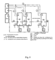
- Fig. 1 shows the additional extensions.
- B1 - Bn are here the programmable components, Z0 - Zn additional components.
- Z0 and Zm may e.g. Plug, Z1 - Zn resistors or capacitors.
- Z0 and Zm could also be parts of a complex charging logic consisting of flash memory, controllers and a microprocessor interface (MPU).
- MPU microprocessor interface
- U denotes the power supply and connections of some pins for setting certain internal operation modes. For XILINX FPGAs, these can be pins M0-M2, which are used to determine the charge protocol. All marked connections are necessary, additional connections.
- the object of this invention is to provide methods by which these circuit parts can be inserted automatically on the entire assembly due to individual constraints and requirements of the developer.
- the invention thus provides a method for designing an electronic circuit on an assembly with at least one field-programmable component, FPGA, which is intended to realize at least a part of the electronic circuit, wherein the electronic circuit comprises a logic part and an extension part, wherein the logic part in at least one FPGA is implemented and the extension part is independent of the logic part, characterized in that at least a part of the extension part is taken from data in a database.
- FPGA field-programmable component
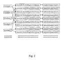
- the data of the database may be divided into two groups, the first group containing those extensions relating to devices and the second group containing those extensions relating to connections between devices.
- the first group may be divided into component-specific extensions and component-common extensions.
- the second group may be subdivided into connection individual extensions, in parallel connection extensions, and in daisy chain connection extensions.
- the extension part may additionally have data relating to the power supply and / or means for setting modes of the at least one FPGA.
- the extension part can each contain generic circuit descriptions and associated implementation instructions.
- the assembly may comprise a circuit carrier, in particular a printed circuit board.
- the part of the electronic circuit realized in the at least one FPGA can be determined for later realization in at least one application-specific integrated circuit.
- the invention also includes a database constructed with the inventive method of constructing a database.
- An advantage of the invention is that the input of these module-level expansions can be made based on the requirements without the user having to worry about the technical implementation.
- Requirements may e.g. the implementation of the load logic such as JTAG, serial or parallel.
- a "generic description of the extension” is e.g. the connections according to point 2.
- the implementation regulation includes i.a. the connection pins for the blocks.
- the extensions are stored according to the above classification according to components and connections. This may look like this: Necessary components for this extension. This can be both individual and shared.
- the connections between new components (Z0 and Zm) are saved in the form of a circuit description in the database.
- Connection points for the components to be expanded Here it is determined which connection of the newly inserted components goes to which connection of the programmable components and in what form the connection is to be realized. This can be individual, parallel or concatenated.
Landscapes
- Engineering & Computer Science (AREA)
- Computer Hardware Design (AREA)
- Physics & Mathematics (AREA)
- Theoretical Computer Science (AREA)
- Evolutionary Computation (AREA)
- Geometry (AREA)
- General Engineering & Computer Science (AREA)
- General Physics & Mathematics (AREA)
- Design And Manufacture Of Integrated Circuits (AREA)
Priority Applications (1)
| Application Number | Priority Date | Filing Date | Title |
|---|---|---|---|
| EP05109042A EP1770565A1 (fr) | 2005-09-29 | 2005-09-29 | Intégration automatique de circuits FPGA sur une carte imprimée |
Applications Claiming Priority (1)
| Application Number | Priority Date | Filing Date | Title |
|---|---|---|---|
| EP05109042A EP1770565A1 (fr) | 2005-09-29 | 2005-09-29 | Intégration automatique de circuits FPGA sur une carte imprimée |
Publications (1)
| Publication Number | Publication Date |
|---|---|
| EP1770565A1 true EP1770565A1 (fr) | 2007-04-04 |
Family
ID=35613665
Family Applications (1)
| Application Number | Title | Priority Date | Filing Date |
|---|---|---|---|
| EP05109042A Withdrawn EP1770565A1 (fr) | 2005-09-29 | 2005-09-29 | Intégration automatique de circuits FPGA sur une carte imprimée |
Country Status (1)
| Country | Link |
|---|---|
| EP (1) | EP1770565A1 (fr) |
Citations (2)
| Publication number | Priority date | Publication date | Assignee | Title |
|---|---|---|---|---|
| EP0433066A2 (fr) * | 1989-12-15 | 1991-06-19 | Hewlett-Packard Company | Architecture de bibliotheque à symbole commun |
| US6883147B1 (en) * | 2002-11-25 | 2005-04-19 | Xilinx, Inc. | Method and system for generating a circuit design including a peripheral component connected to a bus |
-
2005
- 2005-09-29 EP EP05109042A patent/EP1770565A1/fr not_active Withdrawn
Patent Citations (2)
| Publication number | Priority date | Publication date | Assignee | Title |
|---|---|---|---|---|
| EP0433066A2 (fr) * | 1989-12-15 | 1991-06-19 | Hewlett-Packard Company | Architecture de bibliotheque à symbole commun |
| US6883147B1 (en) * | 2002-11-25 | 2005-04-19 | Xilinx, Inc. | Method and system for generating a circuit design including a peripheral component connected to a bus |
Non-Patent Citations (1)
| Title |
|---|
| BRANSON J ET AL: "A SIMPLISTIC PRINTED CIRCUIT BOARD FABRICATION PROCESS FOR COURSE PROJECTS", IEEE TRANSACTIONS ON EDUCATION, IEEE SERVICE CENTER, PISCATAWAY, NJ, US, vol. 43, no. 3, August 2000 (2000-08-01), pages 257 - 261, XP001130007, ISSN: 0018-9359 * |
Similar Documents
| Publication | Publication Date | Title |
|---|---|---|
| EP0642094B1 (fr) | Méthode de programmation d'un module logique | |
| DE69907930T2 (de) | Integrierte Schaltung mit Kalibriermitteln zur Kalibrierung eines elektronischen Moduls und Verfahren zum Kalibrieren eines elektronischen Moduls in einer Integrierten Schaltung | |
| EP3782354B1 (fr) | Procédé de communication entre une application et une machine dans un processus de fabrication | |
| EP1450223B1 (fr) | Circuit d'interface universel configurable pour formé l'interface d'entrée/sortie d'un processus | |
| EP3520350B1 (fr) | Système et procédé de détermination ou de surveillance d'une grandeur de processus dans une installation du domaine de l'automatisation | |
| EP2990892B1 (fr) | Procédé de liaison d'une interface d'entrée/de sortie d'un appareil d'essai destiné à l'essai d'un appareil de commande | |
| DE102017208831A1 (de) | Verarbeitung von Prozessdaten | |
| WO2005119381A1 (fr) | Systeme d'utilisation d'une installation par edition d'objets graphiques | |
| DE4327660C2 (de) | Vorrichtung zum Herstellen einer und Herstellungsverfahren für eine integrierte Halbleiterschaltungsvorrichtung und elektronische Schaltungsvorrichtung | |
| EP1454201B1 (fr) | Systeme d'ingenierie et systeme d'automatisation | |
| DE102006020562A1 (de) | Anordnung und Verfahren zur Reprogrammierung von Steuergeräten | |
| EP1068580B1 (fr) | Procede de comparaison de circuits electriques | |
| DE60003847T2 (de) | Universelle vorrichtung sowie verfahren und werkzeuge zu ihrer verwendung | |
| DE102016118269A1 (de) | Verfahren und System zum verteilten Speichern von Informationen in einer eine Vielzahl von Feldgeräten aufweisenden Anlage der Prozessautomatisierung | |
| WO2004072743A2 (fr) | Automate programmable electrique et procede pour regler les fonctions de cet automate programmable electrique | |
| EP3534225B1 (fr) | Groupe d'assemblage pour l'automatisation de processus industrielle et procédés de fonctionnement et de conception | |
| EP0888588A1 (fr) | Segment ou interface de bus pour connecter un module d'une commande programmable a un bus | |
| EP3115859B1 (fr) | Procédé et système de configuration pour la configuration de sous-ensembles matériels dans un système d'automatisation | |
| EP2965157A1 (fr) | Procédé et dispositif permettant de faire fonctionner une installation de traitement et/ou de fabrication | |
| EP0303065B1 (fr) | Procédé et aménagement de circuit pour modules à semi-conducteurs avec éléments logiques de commutation intégrés en technologie LSI | |
| EP3874334B1 (fr) | Dispositif et procédé de conception de projets itératifs et interactifs d'une station d'e/s pour une commande d'automatisation | |
| EP1770564A1 (fr) | Concéption d'un circuit électronique | |
| DE102017101700A1 (de) | Verfahren zur zeitlich synchronisierten Ausgabe und/oder zeitlich synchronisierten Verarbeitung von Signalen | |
| DE3344007C2 (de) | Taktgesteuertes Programmsteuerwerk | |
| DE102006011286B4 (de) | Schaltungsanordnung zur Gewinnung synchroner Zeitsignale |
Legal Events
| Date | Code | Title | Description |
|---|---|---|---|
| PUAI | Public reference made under article 153(3) epc to a published international application that has entered the european phase |
Free format text: ORIGINAL CODE: 0009012 |
|
| AK | Designated contracting states |
Kind code of ref document: A1 Designated state(s): AT BE BG CH CY CZ DE DK EE ES FI FR GB GR HU IE IS IT LI LT LU LV MC NL PL PT RO SE SI SK TR |
|
| AX | Request for extension of the european patent |
Extension state: AL BA HR MK YU |
|
| AKX | Designation fees paid | ||
| STAA | Information on the status of an ep patent application or granted ep patent |
Free format text: STATUS: THE APPLICATION IS DEEMED TO BE WITHDRAWN |
|
| 18D | Application deemed to be withdrawn |
Effective date: 20071005 |
|
| REG | Reference to a national code |
Ref country code: DE Ref legal event code: 8566 |