EP1770836A2 - Dispositif diode à laser, assemblage avec au moins un dispositif diode à laser, et laser pompé optiquement - Google Patents
Dispositif diode à laser, assemblage avec au moins un dispositif diode à laser, et laser pompé optiquement Download PDFInfo
- Publication number
- EP1770836A2 EP1770836A2 EP06019936A EP06019936A EP1770836A2 EP 1770836 A2 EP1770836 A2 EP 1770836A2 EP 06019936 A EP06019936 A EP 06019936A EP 06019936 A EP06019936 A EP 06019936A EP 1770836 A2 EP1770836 A2 EP 1770836A2
- Authority
- EP
- European Patent Office
- Prior art keywords
- laser diode
- laser
- diode device
- active
- active regions
- Prior art date
- Legal status (The legal status is an assumption and is not a legal conclusion. Google has not performed a legal analysis and makes no representation as to the accuracy of the status listed.)
- Granted
Links
Images



Classifications
-
- H—ELECTRICITY
- H01—ELECTRIC ELEMENTS
- H01S—DEVICES USING THE PROCESS OF LIGHT AMPLIFICATION BY STIMULATED EMISSION OF RADIATION [LASER] TO AMPLIFY OR GENERATE LIGHT; DEVICES USING STIMULATED EMISSION OF ELECTROMAGNETIC RADIATION IN WAVE RANGES OTHER THAN OPTICAL
- H01S5/00—Semiconductor lasers
- H01S5/40—Arrangement of two or more semiconductor lasers, not provided for in groups H01S5/02 - H01S5/30
- H01S5/4025—Array arrangements, e.g. constituted by discrete laser diodes or laser bar
- H01S5/4031—Edge-emitting structures
-
- H—ELECTRICITY
- H01—ELECTRIC ELEMENTS
- H01S—DEVICES USING THE PROCESS OF LIGHT AMPLIFICATION BY STIMULATED EMISSION OF RADIATION [LASER] TO AMPLIFY OR GENERATE LIGHT; DEVICES USING STIMULATED EMISSION OF ELECTROMAGNETIC RADIATION IN WAVE RANGES OTHER THAN OPTICAL
- H01S5/00—Semiconductor lasers
- H01S5/02—Structural details or components not essential to laser action
- H01S5/024—Arrangements for thermal management
- H01S5/02461—Structure or details of the laser chip to manipulate the heat flow, e.g. passive layers in the chip with a low heat conductivity
-
- H—ELECTRICITY
- H01—ELECTRIC ELEMENTS
- H01S—DEVICES USING THE PROCESS OF LIGHT AMPLIFICATION BY STIMULATED EMISSION OF RADIATION [LASER] TO AMPLIFY OR GENERATE LIGHT; DEVICES USING STIMULATED EMISSION OF ELECTROMAGNETIC RADIATION IN WAVE RANGES OTHER THAN OPTICAL
- H01S5/00—Semiconductor lasers
- H01S5/02—Structural details or components not essential to laser action
- H01S5/026—Monolithically integrated components, e.g. waveguides, monitoring photo-detectors, drivers
-
- H—ELECTRICITY
- H01—ELECTRIC ELEMENTS
- H01S—DEVICES USING THE PROCESS OF LIGHT AMPLIFICATION BY STIMULATED EMISSION OF RADIATION [LASER] TO AMPLIFY OR GENERATE LIGHT; DEVICES USING STIMULATED EMISSION OF ELECTROMAGNETIC RADIATION IN WAVE RANGES OTHER THAN OPTICAL
- H01S5/00—Semiconductor lasers
- H01S5/0014—Measuring characteristics or properties thereof
-
- H—ELECTRICITY
- H01—ELECTRIC ELEMENTS
- H01S—DEVICES USING THE PROCESS OF LIGHT AMPLIFICATION BY STIMULATED EMISSION OF RADIATION [LASER] TO AMPLIFY OR GENERATE LIGHT; DEVICES USING STIMULATED EMISSION OF ELECTROMAGNETIC RADIATION IN WAVE RANGES OTHER THAN OPTICAL
- H01S5/00—Semiconductor lasers
- H01S5/02—Structural details or components not essential to laser action
- H01S5/022—Mountings; Housings
- H01S5/0233—Mounting configuration of laser chips
- H01S5/0234—Up-side down mountings, e.g. Flip-chip, epi-side down mountings or junction down mountings
-
- H—ELECTRICITY
- H01—ELECTRIC ELEMENTS
- H01S—DEVICES USING THE PROCESS OF LIGHT AMPLIFICATION BY STIMULATED EMISSION OF RADIATION [LASER] TO AMPLIFY OR GENERATE LIGHT; DEVICES USING STIMULATED EMISSION OF ELECTROMAGNETIC RADIATION IN WAVE RANGES OTHER THAN OPTICAL
- H01S5/00—Semiconductor lasers
- H01S5/02—Structural details or components not essential to laser action
- H01S5/022—Mountings; Housings
- H01S5/0233—Mounting configuration of laser chips
- H01S5/02345—Wire-bonding
-
- H—ELECTRICITY
- H01—ELECTRIC ELEMENTS
- H01S—DEVICES USING THE PROCESS OF LIGHT AMPLIFICATION BY STIMULATED EMISSION OF RADIATION [LASER] TO AMPLIFY OR GENERATE LIGHT; DEVICES USING STIMULATED EMISSION OF ELECTROMAGNETIC RADIATION IN WAVE RANGES OTHER THAN OPTICAL
- H01S5/00—Semiconductor lasers
- H01S5/04—Processes or apparatus for excitation, e.g. pumping, e.g. by electron beams
- H01S5/041—Optical pumping
-
- H—ELECTRICITY
- H01—ELECTRIC ELEMENTS
- H01S—DEVICES USING THE PROCESS OF LIGHT AMPLIFICATION BY STIMULATED EMISSION OF RADIATION [LASER] TO AMPLIFY OR GENERATE LIGHT; DEVICES USING STIMULATED EMISSION OF ELECTROMAGNETIC RADIATION IN WAVE RANGES OTHER THAN OPTICAL
- H01S5/00—Semiconductor lasers
- H01S5/10—Construction or shape of the optical resonator, e.g. extended or external cavity, coupled cavities, bent-guide, varying width, thickness or composition of the active region
- H01S5/14—External cavity lasers
- H01S5/141—External cavity lasers using a wavelength selective device, e.g. a grating or etalon
-
- H—ELECTRICITY
- H01—ELECTRIC ELEMENTS
- H01S—DEVICES USING THE PROCESS OF LIGHT AMPLIFICATION BY STIMULATED EMISSION OF RADIATION [LASER] TO AMPLIFY OR GENERATE LIGHT; DEVICES USING STIMULATED EMISSION OF ELECTROMAGNETIC RADIATION IN WAVE RANGES OTHER THAN OPTICAL
- H01S5/00—Semiconductor lasers
- H01S5/10—Construction or shape of the optical resonator, e.g. extended or external cavity, coupled cavities, bent-guide, varying width, thickness or composition of the active region
- H01S5/18—Surface-emitting [SE] lasers, e.g. having both horizontal and vertical cavities
- H01S5/183—Surface-emitting [SE] lasers, e.g. having both horizontal and vertical cavities having only vertical cavities, e.g. vertical cavity surface-emitting lasers [VCSEL]
Definitions
- the present invention relates to a laser diode device having a plurality of radiation generating suitable active regions and a laser assembly comprising such a laser diode device. Furthermore, the invention relates to an optically pumped laser.
- the peak wavelength of the radiation generated in a single active region of a laser diode chip often has a significant temperature response, i. H. it changes with the operating temperature of the active area.
- the peak wavelength typically changes by about 0.3 nm / K.
- the operating temperature is largely determined by the heat loss generated in the generation of radiation, with the amount of heat loss in the case of electrically pumped lasers being dependent on the conversion efficiency of electrical power to radiant power in the active region of the laser diode.
- different active regions may have different operating temperatures. This can lead to an increase in differences in the peak wavelengths of the radiation generated in the respective active regions or can be responsible for the emergence of such differences.
- An object of the present invention is to provide a laser diode device having a plurality of active regions and a laser device having such a Specify laser diode device, wherein the laser diode device or the laser device is simplified with reduced variation between the operating temperatures of different active areas operable. Furthermore, an optically pumped laser is to be specified, which is simplified pumpable efficiently.
- a laser diode device comprises a plurality of active regions which are arranged laterally next to one another and are suitable for generating radiation, wherein a transverse dimension of the active regions varies in the lateral direction and / or the spacing of adjacent active regions varies in the lateral direction.
- the active regions are expediently designed for generating radiation during operation of the laser diode device.
- the laser diode device preferably has a lateral main extension direction.
- the active regions are particularly preferably arranged in the main extension direction next to one another.
- the radiation-generating active surface of the respective active region can be varied.
- the amount of heat loss incurred in the respective active area can be influenced in a targeted manner.
- the larger the radiation-generating area the greater is the amount of heat loss generated in the respective active area and, accordingly, the operating temperature of the respective active area.
- the operating temperature distribution over the active regions of the laser diode device can be influenced in a targeted manner.
- the operating temperatures of two adjacent active areas typically increase with decreasing the distance between these active areas due to the locally more concentrated loss heat generation.
- a predetermined distribution of the operating temperature of the different active regions of the laser diode device in the lateral direction can be achieved in a simplified manner.
- the operating temperature distribution is formed by appropriate arrangement and / or formation of the active regions such that sets a predetermined operating temperature distribution.
- the active regions are arranged and / or formed such that, during operation of the laser diode device, an operating temperature distribution over different active regions occurs along a main lateral extension direction of the laser diode device compared to another laser diode device, e.g. having equidistantly arranged active regions each having the same transverse dimension, is more homogeneous. In this way, an operating temperature-stabilized laser diode device can be formed.
- the active areas may be arranged and / or formed such that the operating temperature of the active areas is equal at corresponding, equally-selected locations of the respective active areas.
- a reference laser diode device can be manufactured which has equidistantly arranged active regions of the same transverse dimensions. Subsequently, the operating temperature distribution of the reference laser diode device can be measured. In regions of the reference laser diode device in which the active regions have a comparatively low operating temperature, the operating temperature-stabilized laser diode device to be produced below is formed with active regions that have an increased transverse dimension and / or reduced distance compared to those of the reference laser diode device. In contrast to the active regions of low operating temperature of the reference laser diode device in the operating temperature-stabilized laser diode device in this field Laser diode device selectively generates an increased amount of heat loss. This results in a correspondingly increased operating temperature in the respective active regions of the operating temperature-stabilized laser diode device.
- the peak wavelengths of the laser radiation generated by the active regions of the laser diode device can be stabilized.
- the emission spectrum of the laser diode device can thus be narrowed down from an emission spectrum of a laser diode device having an inhomogeneous operating temperature distribution over different active regions due to the stabilization of the peak wavelengths. This is particularly advantageous in applications for which a narrow-band emission spectrum is expedient.
- a narrow-band emission spectrum is advantageous, for example, in pumping applications in which a laser diode device is used for optically pumping a further radiation source, for example a laser.
- a laser to be pumped in this way can be embodied as a solid-state laser, for example as a solid-state disk laser or solid-state laser, as a fiber laser, or as a semiconductor laser, for example as an external cavity semiconductor laser and / or as a semiconductor disk laser.
- Lasers to be optically pumped generally have a comparatively narrow-band absorption spectrum in the medium of the laser to be pumped on. Broadening the emission characteristics of the laser diode device thus reduces the pumping efficiency of the laser diode array used as a pump laser. Such a broadening of the emission spectrum can be counteracted by the inventive design of the laser diode device.
- the operating temperature distribution could also be homogenized by increasing the efficiency of the active regions in the radiation generation with correspondingly reduced heat loss generation.
- this is comparatively complicated or expensive compared to a variation of the transverse dimension of the active regions or the spacing of adjacent active regions.
- the laser diode device has at least one, the laser diode device laterally limiting side surface.
- the operating temperature of the arranged in this area of the laser diode device active areas for. B. due to better heat dissipation or reduced heat loss generation, often less than in areas further away from the side surface.
- the transverse dimension of one active region is greater than the transverse dimension of another active region, which active region is adjacent to the former active region and further spaced from the side surface than the former active region
- the distance between the active areas of a pair with two adjacent active Areas preferably less than the distance between the active areas of another pair with two adjacent active areas, which has a greater distance to the side surface than the former pair.
- at least one active region of the further pair has a larger distance to the side surface than each active region of the former pair.
- both pairs may have a common active area. In the region of the side surface, an increased amount of waste heat can thus be generated in a simplified manner, as a result of which the operating temperature in the active regions of the laser diode device arranged close to the side surface can be purposefully increased.
- the, in particular respective, transverse dimension of the active regions decreases with increasing distance of the active regions from the lateral surface, in particular stepwise.
- the, in particular respective, distance between adjacent active regions preferably increases with increasing distance of the active regions from the lateral surface, in particular stepwise.
- the loss of heat occurring in the active areas relatively far away from the side surface can be reduced in a simplified manner by this arrangement, as can the operating temperature of these active areas. In this way, a homogeneous operating temperature distribution over the active regions of the laser diode device in the lateral direction can be achieved in a simplified manner.
- the laser diode device comprises four or more, preferably ten or more, active regions. Fluctuations in The operating temperature distribution between individual active regions occur increasingly in such a laser diode device due to the large number of active region. Homogenization of the operating temperature distribution is therefore particularly noticeable in this case.
- the active regions of the laser diode device are arranged on a common substrate.
- the laser diode device is thereby particularly compact formable, wherein the substrate preferably mechanically stabilizes the active regions. Since, in such a compact design of the laser diode device, inhomogeneities in the operating temperature distribution of the active regions are particularly noticeable, homogenization of the operating temperature in this case is of particular advantage.
- the side surface which delimits the laser diode device in the lateral direction is preferably formed at least in regions by the substrate.
- the active region closest to the side surface in particular the active region closest to the region of the side surface formed by the substrate, preferably has of the side surface is less than or equal to one of the distances between two adjacent active regions.
- the distance between the active area closest to the side surface and the side area is smaller than the distance between this active area and an active area adjacent to this active area, which is preferably arranged on the side of the active area closest to the side area ,
- the distance between the region of the side surface formed by the substrate and the nearest active region is preferably smaller than the smallest of the distances between the active regions. If the distance between the active regions of the laser diode device varies, the operating temperatures of the active regions can be adjusted to one another in a simplified manner in this way. Optionally, an active area adjacent to the side surface and / or flush with the side surface.
- the active regions are arranged axially symmetrical to an axis of symmetry of the laser diode device.
- the axis of symmetry is perpendicular to the lateral main extension direction of the laser diode device or extends substantially parallel to a surface of the substrate on which the active regions are arranged.
- two active regions of the laser diode device in particular all regions of the laser diode device, belong in each case to discrete laser diode chips. These chips are expediently on attached to the substrate.
- the substrate is preferably formed by a heat sink or a submount.
- the submount is preferably designed as a heat spreader.
- the heat spreader is particularly preferably arranged between the laser diode chips and an additionally provided heat sink.
- the submount is preferably adapted to a thermal expansion coefficient of the laser diode chips, which are preferably made similar.
- the stabilization of the operating temperature can be achieved in a particularly simple manner by appropriate choice of the distances between the individual chips in the assembly of the chips on the substrate.
- the active regions and in particular the individual laser diode chips are spaced apart by a free space.
- the laser diode chips are preferably formed according to edge-emitting lasers.
- two active regions belong to a common laser diode chip, in particular a laser diode bar.
- the substrate in this case is preferably formed by the growth substrate for the active regions of the laser diode chip or formed from the growth substrate.
- the laser diode device is designed as a laser diode chip.
- Two active regions of the laser diode chip may in this case be formed by regions of a continuous active layer, which are preferably part of a semiconductor layer sequence of the laser diode chip, and are energized discretely from one another.
- two active regions of the laser diode chip be spaced apart by a free space.
- the active regions can be formed in semiconductor bodies which are spaced apart from one another by a free space.
- active regions of the laser diode chip are either formed as regions of a continuous active layer which are energized discretely from one another or are spaced apart from one another by a free space.
- a homogenization of the operating temperature distribution can be achieved by suitable design of electrical contacts, for example contact metallizations, for energizing the respective active region.
- the contacts may be arranged like a strip and in particular next to each other on the active layer.
- the contact assigned to the respective active region preferably covers this active region at least partially, particularly preferably completely.
- a semiconductor layer sequence with an active layer can be patterned by means of a suitable mask such that the transverse dimension and / or the distances of adjacent active regions - e.g. discrete subregions of the active layer before structuring - varies across the chip.
- the active regions in particular a semiconductor layer structure comprising the respective active region, are preferably formed for an edge-emitting laser structure.
- Edge emitting laser structures emit radiation substantially parallel to the active region.
- the active regions are preferably similar, d. H. for generating radiation of the same peak wavelength at the same operating temperatures.
- the active regions, in particular the active layer may for example be epitaxially grown on the substrate, which then serves as a growth substrate.
- a laser diode bar is often used to generate high radiation power and accordingly operated with high electrical power. Because of the high electrical power consumption, the peak wavelengths of the radiations produced in different active regions may vary significantly with insufficient stabilization of the operating temperature distribution across the active regions in a laser diode bar. This can be avoided within the scope of the invention.
- a laser device comprises at least one laser diode device having a side surface laterally delimiting the laser diode device and a plurality of laterally adjacent radiation generating active regions, the laser diode device being disposed on a support, the distance between the side surface and a side surface support laterally delimiting edge is less than the distance between the active region nearest the side surface and the side surface and / or the distance between the side surface and the edge is less than one of the distances between two adjacent active regions of the laser diode device
- the active regions are expediently designed for generating radiation during operation of the laser diode device.
- the carrier of the laser diode device is thus adapted to the dimension of the laser diode device.
- the carrier is adapted to the laser diode device such that the lateral heat flow expansion, in particular in the carrier, is reduced.
- the operating temperature distribution over the active regions of the laser diode device can be influenced.
- dissipated dissipation heat is subject in the carrier, due to the relatively close arrangement of side surface and support edge relative to each other, only a relatively small lateral edge heat flow expansion.
- the operating temperature of the comparatively close to the Side lying lying active areas is not significantly reduced - compared to the operating temperature of the side surface remote active areas - due to the only moderate heat flux expansion in the carrier.
- the operating temperatures of the active regions can be adjusted to one another in a simplified manner relative to the carrier via such an arrangement of the laser diode device. By way of this, as already described above, the peak wavelengths of the radiations generated in the various active regions can be stabilized.
- the carrier preferably limits the laser arrangement at least partially in the lateral direction.
- An arrangement of the side surface as close as possible to the edge of the carrier has proven to be particularly advantageous for a reduction or complete avoidance of the marginal heat flow expansion.
- the distance of the side surface from the edge is less than the smallest of the distances between the active regions of the laser diode device.
- the side surface, in particular on its side facing the carrier is flush with the carrier. A heat flow expansion in the lateral direction in the carrier can thus be substantially completely avoided.
- the carrier is preferably designed as a heat sink or in particular as a submount. In the active areas resulting heat loss can be so reliably routed away from the active areas.
- the submount may optionally between the laser diode device and another Laser arrangement carrier, such as a heat sink, be arranged.
- the submount is better adapted to the thermal expansion coefficient of an element of the laser diode device on the submount side of the laser diode device.
- the carrier can therefore be adapted to the thermal expansion coefficient of the laser diode device, in particular with regard to the coefficient of thermal expansion, for example with a deviation of 5% or less. The risk of thermally induced damage to the laser diode device can thus be reduced.
- a copper-tungsten (CuWo) containing submount is particularly suitable.
- CuWo copper-tungsten
- the thermal expansion coefficient of such a heat spreader can be changed and adapted to the thermal expansion coefficient of the laser diode device, in particular to that of the substrate of the laser diode device or to a semiconductor material arranged on the part of the heat spreader.
- Particularly good thermal matching can be achieved with a GaAs-based laser diode chip, for example with a GaAs-containing (growth) substrate and / or a GaAs-based active region.
- heat sink is particularly suitable for a Cu heat sink.
- the substrate is arranged on the side of the active regions facing away from the carrier.
- the heat dissipation from the active regions into the carrier can be improved as the heat does not have to be conducted through the substrate.
- the substrate is in this case expediently formed by the growth substrate. The risk of damage to the laser diode device due to excessive heat due to heat accumulation can thus be reduced.
- differences in the operating temperatures of the active regions are particularly greatly increased in such an arrangement of the substrate.
- An operating temperature stabilization by means of variation of the transverse dimensions and / or the distances between the active regions and / or a corresponding adaptation of the dimensions of the laser diode device to the carrier are of particular advantage in this case.
- the contacts for the active regions are arranged between the carrier and the active layer.
- the laser diode device of the laser arrangement is preferably designed as a laser diode device according to the invention.
- the operating temperature distribution can thus be further influenced in a simplified manner. Therefore, features described above and in the following in connection with the laser diode device according to the invention can also be used for the laser arrangement according to the invention and vice versa.
- the laser arrangement and the laser diode device can be embodied in a simplified manner with an operating temperature distribution extending in a similar manner in the lateral direction in the active regions. This is particularly noticeable with identically formed active regions which the laser diode device prefers having. These should nominally emit radiation of the same peak wavelength, which, however, may vary due to operating temperature differences. This variation can be reduced or completely eliminated in the invention.
- An operating temperature-stabilized laser diode device or a corresponding laser arrangement is accordingly particularly suitable for a pumping application in which a radiation source to be pumped is optically pumped by absorption of the radiation generated by the laser diode device.
- An optically pumped laser according to the invention is pumped by means of a laser diode device according to the invention or a laser arrangement according to the invention.
- these lasers are particularly suitable as pump lasers for efficient pumping.
- the laser to be pumped is preferably designed as a solid-state laser, in particular as a solid-state disk laser or solid-state laser, as a fiber laser or as a semiconductor laser, in particular as a semiconductor disk laser.
- the pump radiation source is particularly suitable for pumping a semiconductor laser, in particular a surface-emitting semiconductor laser, which is provided for operation with an external resonator.
- the semiconductor laser is embodied as a VECSEL (Vertical External Cavity Surface Emitting Laser) and / or disk laser.
- FIG. 1 shows a laser arrangement 1 on the basis of a schematic sectional view in FIG. 1A and a schematic plan view of the laser arrangement in FIG. 1B.
- the laser arrangement 1 comprises a laser diode chip 2, which comprises a plurality of active regions 4a, 4b, 4c, 4d,..., 4n, which are arranged side by side on a common substrate 3 along a lateral main extension direction R of the laser diode chip and are suitable for generating radiation.
- the laser diode chip 2 comprises ten or more active regions, e.g. twelve active areas.
- an active region is formed respectively in a semiconductor body 5a, 5b, 5c, 5d,..., 5n.
- the semiconductor bodies 5a... 5n are designed as discrete semiconductor structures arranged spatially separated on the substrate 3.
- the semiconductor bodies 5a... 5n are in particular arranged equidistantly on the substrate 3 and have the same transverse dimensions, ie. H. equal widths, along the lateral main extension direction.
- a longitudinal dimension of the semiconductor bodies, i. their length, perpendicular to the lateral main extension direction, is preferably greater than the transverse dimension and particularly preferably constant.
- the active areas preferably have the same area, i. the same active area, up.
- the laser diode chip 2 of the laser arrangement 1 is arranged on a carrier 6, the substrate 3 preferably being arranged between the active regions 4a... 4n and the carrier is.
- the carrier 6 is bounded laterally in the lateral direction by a first edge surface 7 and a second edge surface 8, the second edge surface 8 lying opposite the first edge surface 7.
- the edge surfaces 7, 8 at the same time limit the laser arrangement 1 in the lateral direction.
- the laser diode chip 2 is bounded in the lateral direction by a first side surface 9 and a second side surface 10. These are formed by the substrate 3.
- the second side surface 10 faces the first side surface 9.
- the edge surfaces are spaced from the side surfaces.
- the active areas are spaced from the side surfaces 9 and 10, respectively, so that starting from the active areas, the laser arrangement has a structure that gradually widens laterally.
- the semiconductor bodies 5a... 5n are formed in accordance with edge-emitting laser structures.
- a resonator for such a laser structure can be formed by means of a first reflector surface 11 and a second reflector surface 12, which may be formed by the respective semiconductor body 5a... 5n or which may be formed on the respective semiconductor body.
- a surface of the respective semiconductor body forms the respective reflector surface.
- the first reflector surface 11 preferably has a lower reflectivity than the second reflector surface 12, so that build up during operation of the laser diode chip 2, a radiation field in the resonator of the respective semiconductor body, amplified there and decouple as laser radiation 13 via the reflector surface serving as a coupling surface 11 from the resonator can.
- the semiconductor bodies 5a ... 5n are monolithically integrated.
- the semiconductor bodies can grown epitaxially on the substrate 3.
- the semiconductor bodies are preferably based on GaAs.
- a GaAs substrate is particularly suitable in this case as a substrate, in particular also as a growth substrate for an epitaxial growth of the semiconductor bodies.
- the active regions are preferably identical, in particular designed for emitting laser radiation of the same peak wavelength at the same operating temperature. Particularly suitable for efficient radiation generation are active regions which have a single or multiple quantum structure.
- quantum well structure does not give any indication of the dimensionality. It thus includes u.a. Quantum wells, quantum wires and quantum dots and any combination of these structures.
- Laser diode chips based on (In, Al) GaAs are particularly suitable for generating radiation in the infrared spectral range.
- the carrier 6 for heat dissipation from the laser diode chip is preferably designed as a heat sink.
- the support 6 contains, for example, a metal, for example Cu, or an alloy, for example: CuWo, with advantageously high thermal conductivity. The heat can be dissipated from the active regions via the substrate 3 into the carrier 6.
- the laser assembly 1 can be connected to the carrier 6 on a connection carrier (not shown), e.g. a printed circuit board, arranged and contacted there electrically. An explicit representation of electrical contacts of the laser arrangement has been omitted for reasons of clarity.
- the carrier can serve as a submount for the laser diode chip, which is arranged between the laser diode chip and the connection carrier and / or an additional heat sink.
- resulting heat loss can be conducted in the substrate 3 in a lateral direction to the respective side surface of the substrate.
- Heat coming from the substrate 3 in the vertical direction into the carrier 6 can be conducted laterally in the carrier in the direction of the edge surfaces 9 and 10.
- the heat flow can thus be widened in the substrate or in the carrier in the lateral direction. This is shown schematically in FIG. 1A by the heat flow lines 14 and 15 that expand in the lateral direction.
- the edge regions of the laser diode chip ie, the regions near the side surfaces, a smaller amount of waste heat is generated compared with a central central region of the laser diode chip 2. This heat is increasingly derived from the active areas due to the heat flow expansion and the side surface comparatively large, available for heat dissipation surface area.
- the operating temperatures T a , T b , T c , T d , ... and T n of the active regions 4a, 4b, 4c, 4d, ..., and 4n therefore, increase with increasing distance from the side surfaces 9 and 10 lateral direction.
- the operating temperatures of the active regions are preferably determined at corresponding locations of the respective active region along the lateral main extension direction.
- the operating temperature of an active region in the middle of this active region is determined by the first reflector surface 11.
- the illustration in FIG. 1 corresponds to the semiconductor bodies of individual laser diode chips, the substrate 3 to the chip carrier, which is embodied eg as a heat spreader or submount, and the support 6 of a heat sink or a connection carrier for the chips mounted on the chip carrier.
- a CuWo submount and a Cu heat sink is particularly suitable.
- the individual laser diode chips are preferably designed to generate radiation of the same peak wavelength.
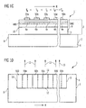
- the laser arrangement 1 shown schematically in FIGS. 1C and 1D essentially corresponds to the laser arrangement illustrated in FIGS. 1A and 1B.
- the laser diode chip 2 has a semiconductor layer structure 500 with a continuous active layer 400, which is arranged on the substrate 3.
- the semiconductor layer structure 500 preferably terminates flush with the side surfaces 9, 10 of the substrate 3.
- the active regions 4a... 4n of the laser diode chip 2 are formed by regions of the active layer 400 that are discretely energized in the operation of the semiconductor chip.
- the reflector surfaces 11, 12 are further formed by a continuous surface.
- the active areas 4a... 4n are each covered by an electrical contact, in particular a contact metallization. Preferably, exactly one contact is assigned to each active area.
- the discrete contacts 50a... 50n correspond in their shape and arrangement to the semiconductor bodies 5a... 5n according to FIGS. 1A and 1B, respectively.
- the contacts 50a... 50n are arranged equidistantly in the lateral direction on the semiconductor layer structure 500.
- the active regions 4a... 4n which generate radiation during operation of the laser diode chip 2 are likewise arranged equidistantly.
- the contacts are formed as, in particular parallel to each other, contact strips.
- the contacts continue to have the same widths.
- the operating temperature distribution in the lateral direction in the laser diode chip 2 shown in FIGS. 1C and 1D can also be inhomogeneous with those of the chip according to FIGS. 1A and 1B. Due to the continuous semiconductor layer structure, which preferably contains a plurality of further semiconductor layers in addition to the active layer 400, the heat removal from the active regions can be even further inhibited. The fluctuations in the operating temperature may even be increased compared to the active regions spaced apart from each other by a clearance.
- the laser diode chip 2 can be fixed on the carrier 6 by a preferably electrically and / or thermally conductive connecting layer (not shown) and in particular electrically and / or thermally conductively connected to the carrier 6.
- the connection layer is preferably arranged between the laser diode chip and the carrier 6.
- the connecting layer can be embodied as a solder layer, in particular as an in-solder layer.
- the active regions may be arranged between the carrier 6 and the substrate 3.
- the contacts 50a... 50n may be arranged between the semiconductor layer structure 500 and the carrier 6 for discrete energization of the active layer (FIG. 1E).
- the Heat dissipation from the active areas can be improved. The risk of damage due to excessive temperatures damage to the laser diode chip during operation of the laser assembly 1 is reduced. Since the thermal connection to the carrier 6 is improved in such a configuration, a lateral heat flow widening in the carrier is also increasingly noticeable. As a result, the fluctuations in the peak wavelengths are further enhanced.
- the laser diode chips shown in FIGS. 1A to 1E are preferably designed as laser diode bars.
- Figure 1F quantitatively shows the operating temperature profile, i. the change in the operating temperature ⁇ T in ° C along the distance x in ⁇ m along the main lateral extension direction, starting from the center of the laser diode chip towards the side surface 9 of the substrate 3 for a laser arrangement similar to those in Figures 1A, 1B and 1C, 1D and 1E shows arrangements for different fill factors F of the active region substrate. The decrease in operating temperatures in the direction of the side surface can be clearly seen.
- the peak wavelength of the radiation generated in the respective active region depends on its operating temperature, this gradient of the operating temperature leads to different peak wavelengths of the radiation generated in the respective active regions.
- the emission spectrum of the laser diode chip 2 is thus widened due to the temperature dependence of the peak wavelength. This can be for applications of the laser arrangement, such as for pumping a solid-state laser, which is usually a narrow one Absorption spectrum, be undesirable.
- the peak wavelength can change by 0.3 nm / K, so that differences in operating temperature between different active regions of up to about 40 K, which can result in a lateral direction, can significantly affect the width of the emission spectrum of the laser diode chip ,
- this operating temperature gradient-induced peak wavelength shift can be counteracted within the scope of the invention.
- FIG. 2 shows an exemplary embodiment of a laser arrangement 1 on the basis of a schematic plan view in FIG. 2A and a schematic sectional view in FIG. 2B.
- the laser assembly 1 corresponds to the laser arrangement shown in Figs. 1A and 1B.
- elements of the laser arrangement are matched to one another such that the operating temperature distribution in the active regions is homogenized in the lateral direction.
- the active regions preferably have the same operating temperatures T a , T b , T c , T d ,..., T n in the lateral direction at corresponding locations in the respective active region.
- the substrate 3 terminates flush with the carrier 6 in the lateral direction.
- the edge surface 7 of the carrier and the side surface 9 of the substrate or the edge surface 8 and the side surface 10 close to each other flush and preferably each form a continuous, more preferably a flat Surface off.
- Both the substrate 3 and the carrier 6 delimits the laser arrangement 1 in the lateral direction. Furthermore, the active regions 4a and 4n and the semiconductor bodies 5a and 5n adjoin the side surfaces 10 and 9, respectively. The semiconductor bodies 5n and 5a arranged on the side surfaces 9 and 10 can in particular terminate flush with the substrate 3.
- a lateral heat flow expansion in the region of the side surfaces 9, 10 and the edge surfaces 7, 8 can be avoided.
- the operating temperature stabilization in the lateral direction is simplified as a result, since the operating temperature of the peripherally arranged active areas due to the suppression of the heat flow expansion is equalized to those of the active areas further away from the side surfaces. This is illustrated by the heat flow lines 14 and 15 which, in contrast to the lines in FIG. 1, are essentially straight lines and extend in a vertical direction from the active region into the carrier.
- the active areas 4a and 4n which are closest to the side surfaces 10 and 9 respectively, may also be spaced laterally from these side surfaces.
- this distance is preferably smaller than that between two adjacent active regions of the laser diode chip.
- the distance to the side surface in the lateral direction is preferably smaller than the distance of the active region nearest the respective side surface from the active region adjacent to this (approximately smaller than the distance of the regions 4a and 4b).
- Particularly preferred is the distance of the respective side surface nearest active Area to this side surface smaller than the smallest of the distances between the active areas of the laser diode chip.
- the distances or the transverse dimensions of the active regions can be varied (see the description of the following exemplary embodiments).
- the side surfaces 9 and 10 may be spaced from the edge surfaces 7 and 8 in the lateral direction. In order to prevent a significant heat flow widening in the carrier 6, this distance is preferably smaller than one of the distances between two adjacent active regions of the laser diode chip and / or smaller than the distance of the active region closest to the respective side surface from this side surface.
- the operating temperature could be kept essentially constant at corresponding locations in different active regions via such tuning of the laser diode chip and the carrier, while in a laser arrangement with a reference laser diode chip similar to that shown in FIG 1, the operating temperature fluctuated about 38K. At a distance of the semiconductor body of 200 microns, the fluctuation of the operating temperature in the reference laser diode chip was about 33 K. Also this fluctuation could be compensated.
- a corresponding compensation of the fluctuation in the operating temperature due to the adaptation of the laser diode chip 2 to the dimension of the carrier could also be achieved with a laser arrangement according to FIGS. 1C and 1D or 1E.
- the peripheral contacts 50a and 50n are In this case, preferably in the lateral direction as close as possible to the side surfaces 9, 10 of the substrate 3, and in particular at the edge of the semiconductor layer structure 500, corresponding to the semiconductor bodies 5a and 5n.
- the edge-side active regions are advantageously formed as close as possible to the carrier edge or the substrate edge. A heat flow expansion can be so particularly efficiently prevented.
- FIG. 3A shows an exemplary embodiment of a laser diode chip 2 on the basis of a schematic plan view.
- the laser diode chip 2 substantially corresponds to the laser diode chip described in connection with FIGS. 1A and 1B.
- the semiconductor bodies 5a... 51 having the active regions are not arranged equidistantly along the lateral main extension direction R.
- the distances D ab , D bc , D cd , D de , D ef or D fg between two adjacent semiconductor bodies increase with increasing distance of the semiconductor body from the respective side surface 10 and 9 of the substrate 3 (D from ⁇ D bc ⁇ D cd ).
- the linear occupation density of the laser diode chip 2 with active regions accordingly decreases in the lateral direction with increasing distance from the respective side surface.
- linear occupation density is understood to mean the ratio of the distances covered by active regions during the sweeping of the laser diode chip along the main lateral extent direction R of the laser diode chip to the total distance swept along the main longitudinal extension direction of the laser diode chip.
- An arrangement of the active regions or the semiconductor bodies on the substrate 3 axisymmetric to the axis of symmetry 16 of the laser diode chip 2, which is perpendicular to the lateral main extension direction R and / or parallel to that surface of the substrate 3, on which the semiconductor body is arranged runs, is for a homogeneous operating temperature distribution in the lateral direction of particular advantage.
- the semiconductor bodies or the active regions are therefore preferably arranged symmetrically with respect to this axis of symmetry 16.
- the entire laser diode chip 2 is formed axially symmetrical to this axis.
- an operating temperature profile extending laterally in the active regions can be realized.
- the distance between adjacent active areas in particular in Steps of a predetermined size, between a smallest of the distances of adjacent active areas of D / 3, preferably D / 5, more preferably D / 10, and a maximum of the distances of adjacent active areas D to vary.
- a corresponding homogenization of the operating temperature of the active regions can also be achieved in the case of a laser diode chip 2 whose active regions are formed by regions of a continuous active layer 400 that are discretely energized from one another (compare FIGS. 1C and 1D or 1E).
- the distances between 50a... 501 are varied accordingly. Accordingly, the above statements apply to the embodiment of a laser diode chip 2 shown in schematic plan view in FIG. 3B.
- the explanations for the semiconductor body or the active regions are therefore also applicable in particular to the formation of the contacts.
- the contacts are preferably strip-like in plan view, in particular formed like a rectangle.
- the contacts may have the same widths.
- FIGS. 4A and 4B each show a schematic sectional view through a laser arrangement 1 similar to the laser arrangements shown in FIGS. 1A, 1B and 2.
- the semiconductor bodies 5a... 5g or the active regions of the laser diode chips each have the same widths.
- the operating temperature of the active regions increases from this side face in the lateral direction.
- the spacing of adjacent active areas on the side face 9 with respect to the reference laser diode chip is reduced and increased on the side face 10.
- the active regions preferably each have the same active area.
- FIG. 5 shows an exemplary embodiment of a laser diode chip 2 according to the invention on the basis of a schematic plan view.
- the laser diode chip 2 corresponds to the laser diode chip described in connection with FIG. 3, wherein instead of or in addition to the variation of the distances between the semiconductor bodies 5a... 5k or between the active regions, their transverse dimensions, ie the widths b a k of the semiconductor body or the active regions, vary.
- the active regions accordingly have different widths, but may optionally be arranged equidistantly.
- the widths of the active regions preferably decrease with increasing distance from the side surface 10 of the substrate 3 (b a > b b > b c > b d ).
- An axisymmetric arrangement to the symmetry axis 16 is for a homogeneous, in particular symmetrical, operating temperature profile in turn particularly suitable.
- the largest of the widths of the active regions of the laser diode chip is 1.2 times or more, preferably 1.5 times or more, particularly preferably 2 times or more, the smallest of the widths of the active regions of the laser diode chip in the lateral main extension direction.
- the laser diode chip 2 illustrated in schematic plan view on the basis of FIG. 5B corresponds to the laser diode chip described in connection with FIGS. 1C and 1D or 1E, except for the formation of the contacts.
- the operating temperature distribution is stabilized, in contrast to the semiconductor bodies, as in FIG. 5A, the width of the contacts 50a... 50k has been varied accordingly.
- the comments on the semiconductor bodies can thus also apply to the contact strips, in particular their width.
- the active regions have different active surfaces according to FIG.
- the exemplary embodiments according to FIGS. 3A, 3B, 4B, 5A and 5B, in which the operating temperature distribution is influenced by the configuration or arrangement of the active regions, can be compared to the exemplary embodiment according to FIG. 2, due to the reduced adjustment or tuning effort of the laser diode chip Vehicle, to be realized in a simplified manner.
- masks which are used in the formation of the semiconductor bodies or of the contacts, to the changed dimensions and / or spacings of the semiconductor bodies or of the contacts. This can be dispensed with in a vote of the laser diode chip on the carrier, such as in the embodiment of Figure 2.
- a predetermined operating temperature profile may also be formed over the active regions, which is inhomogeneous, i. the operating temperatures in different active regions, in particular in the lateral direction, can be specifically designed differently from one another.
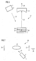
- FIG. 6 shows a schematic view of an exemplary embodiment of an optically pumped semiconductor laser according to the invention.
- the optically pumped semiconductor laser 17 comprises a surface-emitting semiconductor structure 18, which is optically pumped by means of a laser diode chip 2 or a laser arrangement 1 as a pump radiation source, which may be embodied according to one of the preceding embodiments.
- the pump radiation source is arranged such that pump radiation 19 is absorbed in an active zone 20 of the semiconductor laser, for example comprising a quantum well structure.
- the active zone is optically excited to emit radiation of longer wavelengths with respect to the pump radiation which emerges from a surface of the semiconductor structure.
- an external resonator of the semiconductor laser 17 by means of at least one external Mirror 21 is limited, can build up a radiation field 22, which can be amplified in the semiconductor structure 18.
- the resonator is delimited by a further mirror 23, which is preferably monolithically integrated, for example as a Bragg mirror, in the semiconductor structure 18, in particular together with the active zone 20.
- the external mirror 21 is preferably designed as a coupling-out mirror of laser radiation 24 from the resonator.
- the semiconductor laser is designed in particular as an optically pumped VECSEL.
- the semiconductor laser 17 can be pumped very efficiently by means of an operating temperature-stabilized pump radiation source.
- FIG. 7 shows a schematic view of an exemplary embodiment of an optically pumped laser.
- a laser diode chip 2 or a laser arrangement 1 in particular in a design which is stabilized with respect to the operating temperature, is used as pump radiation source.
- the pump radiation 19 is absorbed and re-emitted.
- the re-emitted radiation is amplified in a resonator formed by means of the mirrors 26 and 27 and by means of the amplification medium 25.
- the amplified radiation can decouple out of the resonator as laser radiation 24.
- the laser 28 shown in FIG. 7 is designed, for example, as a solid-state disk laser, solid state laser or as a fiber laser. Due to the usually narrow absorption spectrum in the Amplification medium 25 is a pump having a pump radiation source which, like the operating temperature-stabilized laser arrangement or a correspondingly stabilized laser diode chip, has a narrow emission spectrum, is of particular advantage.
- a corresponding operating temperature stabilization can be achieved by adapting the dimension of the laser diode device with the discrete chips to a thermally conductive (chip) carrier, the variation of the transverse dimensions and / or a variation of the distances of the laser diode chips become.
- an operating temperature stabilization is of particular advantage due to the particularly compact design.
- a laser arrangement in the context of the invention may also comprise a plurality of preferably operating temperature-stabilized laser diode chips.
- the invention may optionally also be applied to other radiation-emitting semiconductor chips, for example LED chips having a plurality of active regions, in particular arranged on a common substrate. Because of the often particularly high power dissipation in semiconductor lasers, however, the invention is particularly suitable for lasers.
Landscapes
- Physics & Mathematics (AREA)
- Condensed Matter Physics & Semiconductors (AREA)
- General Physics & Mathematics (AREA)
- Electromagnetism (AREA)
- Optics & Photonics (AREA)
- Semiconductor Lasers (AREA)
Applications Claiming Priority (1)
| Application Number | Priority Date | Filing Date | Title |
|---|---|---|---|
| DE102005046785 | 2005-09-29 |
Publications (3)
| Publication Number | Publication Date |
|---|---|
| EP1770836A2 true EP1770836A2 (fr) | 2007-04-04 |
| EP1770836A3 EP1770836A3 (fr) | 2010-08-11 |
| EP1770836B1 EP1770836B1 (fr) | 2015-04-22 |
Family
ID=37668723
Family Applications (1)
| Application Number | Title | Priority Date | Filing Date |
|---|---|---|---|
| EP20060019936 Active EP1770836B1 (fr) | 2005-09-29 | 2006-09-22 | Dispositif à diode laser, assemblage avec au moins un dispositif à diode laser, et laser pompé optiquement |
Country Status (4)
| Country | Link |
|---|---|
| US (2) | US7468999B2 (fr) |
| EP (1) | EP1770836B1 (fr) |
| JP (1) | JP2007096326A (fr) |
| FR (1) | FR2893194A1 (fr) |
Families Citing this family (17)
| Publication number | Priority date | Publication date | Assignee | Title |
|---|---|---|---|---|
| US9166130B2 (en) | 2012-10-24 | 2015-10-20 | Spectrasensors, Inc. | Solderless mounting for semiconductor lasers |
| JP4341685B2 (ja) * | 2007-02-22 | 2009-10-07 | セイコーエプソン株式会社 | 光源装置及びプロジェクタ |
| JP5582460B2 (ja) * | 2007-07-13 | 2014-09-03 | 株式会社リコー | 面発光レーザアレイ、光走査装置及び画像形成装置 |
| JP2009054873A (ja) * | 2007-08-28 | 2009-03-12 | Toshiba Corp | 発光素子 |
| JP5521411B2 (ja) * | 2009-07-03 | 2014-06-11 | ソニー株式会社 | 半導体レーザ装置 |
| JP5460477B2 (ja) * | 2010-06-18 | 2014-04-02 | 古河電気工業株式会社 | 面発光レーザアレイ素子 |
| US9368934B2 (en) | 2011-02-14 | 2016-06-14 | Spectrasensors, Inc. | Semiconductor laser mounting for improved frequency stability |
| US9166364B2 (en) * | 2011-02-14 | 2015-10-20 | Spectrasensors, Inc. | Semiconductor laser mounting with intact diffusion barrier layer |
| JP5981092B2 (ja) * | 2011-03-23 | 2016-08-31 | ローム株式会社 | マルチビーム半導体レーザ装置 |
| JP5901391B2 (ja) * | 2012-03-30 | 2016-04-06 | 富士通株式会社 | 光半導体素子、発光装置、光伝送装置及び光半導体素子の製造方法 |
| JP5940214B2 (ja) * | 2013-05-13 | 2016-06-29 | 三菱電機株式会社 | 半導体レーザ装置 |
| JP6244668B2 (ja) * | 2013-05-31 | 2017-12-13 | 住友電気工業株式会社 | 量子カスケードレーザ |
| JP6801091B2 (ja) * | 2016-09-22 | 2020-12-16 | アップル インコーポレイテッドApple Inc. | 磁性膜を利用した結合インダクタ構造 |
| JP7232239B2 (ja) * | 2018-02-26 | 2023-03-02 | パナソニックホールディングス株式会社 | 半導体発光装置 |
| JP7297121B2 (ja) * | 2019-01-10 | 2023-06-23 | 三菱電機株式会社 | 半導体レーザ装置 |
| CN113064136A (zh) | 2020-01-02 | 2021-07-02 | 隆达电子股份有限公司 | 发光元件与发光模块 |
| US20240195146A1 (en) * | 2022-12-13 | 2024-06-13 | Ii-Vi Delaware, Inc. | Monolithic laser arrays with non-uniform laser spacing |
Family Cites Families (14)
| Publication number | Priority date | Publication date | Assignee | Title |
|---|---|---|---|---|
| US4069463A (en) * | 1976-09-02 | 1978-01-17 | International Business Machines Corporation | Injection laser array |
| US4751711A (en) * | 1985-08-16 | 1988-06-14 | Spectra Diode Laboratories, Inc. | Asymmetric offset stripe laser for emission in a single lobe |
| US4901330A (en) * | 1988-07-20 | 1990-02-13 | Amoco Corporation | Optically pumped laser |
| JPH06132610A (ja) * | 1992-10-21 | 1994-05-13 | Nippon Telegr & Teleph Corp <Ntt> | 半導体レーザアレイ素子及びその製造方法 |
| US6058124A (en) * | 1997-11-25 | 2000-05-02 | Xerox Corporation | Monolithic independently addressable Red/IR side by side laser |
| DE10036283A1 (de) * | 2000-07-26 | 2002-02-07 | Bosch Gmbh Robert | Laserdiodenanordnung |
| JP2002335046A (ja) * | 2001-05-10 | 2002-11-22 | Hamamatsu Photonics Kk | 半導体レーザアレイ |
| JP2003069152A (ja) * | 2001-06-15 | 2003-03-07 | Sony Corp | マルチビーム半導体レーザ素子 |
| JP2003031905A (ja) * | 2001-07-12 | 2003-01-31 | Hitachi Ltd | 多ビーム半導体レーザ素子及び半導体レーザ装置 |
| JP3736462B2 (ja) * | 2002-01-17 | 2006-01-18 | ソニー株式会社 | 半導体レーザ装置 |
| US6724792B2 (en) * | 2002-09-12 | 2004-04-20 | The Boeing Company | Laser diode arrays with replaceable laser diode bars and methods of removing and replacing laser diode bars |
| JP2005135933A (ja) * | 2003-10-28 | 2005-05-26 | Sony Corp | 半導体レーザの製造方法 |
| JP4552443B2 (ja) * | 2004-01-27 | 2010-09-29 | 富士ゼロックス株式会社 | 面発光型半導体レーザアレイ |
| US20060018355A1 (en) * | 2004-07-23 | 2006-01-26 | Comlasc.Nt-Ab | Laser diode arrays with reduced heat induced strain and stress |
-
2006
- 2006-09-22 EP EP20060019936 patent/EP1770836B1/fr active Active
- 2006-09-28 US US11/541,131 patent/US7468999B2/en active Active
- 2006-09-28 FR FR0608510A patent/FR2893194A1/fr not_active Withdrawn
- 2006-09-28 JP JP2006265703A patent/JP2007096326A/ja active Pending
-
2008
- 2008-12-23 US US12/343,448 patent/US7933302B2/en active Active
Also Published As
| Publication number | Publication date |
|---|---|
| EP1770836A3 (fr) | 2010-08-11 |
| JP2007096326A (ja) | 2007-04-12 |
| US20070160101A1 (en) | 2007-07-12 |
| FR2893194A1 (fr) | 2007-05-11 |
| US7468999B2 (en) | 2008-12-23 |
| US7933302B2 (en) | 2011-04-26 |
| EP1770836B1 (fr) | 2015-04-22 |
| US20090196316A1 (en) | 2009-08-06 |
Similar Documents
| Publication | Publication Date | Title |
|---|---|---|
| EP1770836B1 (fr) | Dispositif à diode laser, assemblage avec au moins un dispositif à diode laser, et laser pompé optiquement | |
| EP2223399B1 (fr) | Puce laser à semi-conducteur à émission par la tranche comprenant au moins une barrière de courant | |
| EP2564478B1 (fr) | Source de lumière laser | |
| EP1430575B1 (fr) | Laser a semi-conducteur a emission verticale, utilisant le pompage optique | |
| WO2009082999A2 (fr) | Puce laser à semi-conducteur à émission par la tranche comprenant une bande de contact structurée | |
| DE10043896B4 (de) | Laservorrichtung | |
| EP2409368A2 (fr) | Composant semiconducteur optoélectronique | |
| DE112019003830T5 (de) | Lichtemittierende Halbleitervorrichtung und Laservorrichtung vom externen Resonanztyp | |
| EP2218153B1 (fr) | Procédé de fabrication d'un composant émettant un rayonnement et composant émettant un rayonnement | |
| EP1683245B1 (fr) | Vcsel monolithique a pompage optique comprenant un emetteur a emission par la tranche place lateralement | |
| DE10223540B4 (de) | Optisch gepumpte Halbleiterlaservorrichtung | |
| EP1792373B1 (fr) | Laser a semi-conducteurs a emission par la surface a pompage optique lateral avec un dissipateur thermique integree | |
| DE10243545A1 (de) | Optisch gepumpte Halbleiterlaservorrichtung | |
| DE102007053328A1 (de) | Halbleiterlaser mit Fabry-Perot-Resonator | |
| EP4283802A2 (fr) | Diode laser présentant des propriétés électroconductrices améliorées | |
| WO2026052504A1 (fr) | Laser à semi-conducteur et procédé de production d'un laser à semi-conducteur | |
| DE102022102089A1 (de) | Laserpackage und verfahren zur herstellung eines laserpackage | |
| WO2018219667A1 (fr) | Diode laser à semi-conducteurs ayant deux résonateurs | |
| EP4260417B1 (fr) | Diode laser à ouverture thermique intégré | |
| WO2008000243A2 (fr) | Corps semi-conducteur à surface émettrice à sens d'émission vertical et longueur d'ondes à émission stabilisée | |
| DE112021002957B4 (de) | Halbleiterlaser mit horizontalem und vertikalem laserelement, lidar-system und verfahren zur herstellung | |
| DE102006044782A1 (de) | Laserdiodenvorrichtung, Laseranordnung mit mindestens einer Laserdiodenvorrichtung und optisch gepumpter Laser | |
| WO2019121407A1 (fr) | Laser à semi-conducteurs, procédé de fonctionnement pour un laser à semi-conducteurs et procédé de détermination du facteur de remplissage optimal d'un laser à semi-conducteurs | |
| EP1415376B1 (fr) | Laser compose | |
| DE3486103T2 (de) | Halbleiterlaser. |
Legal Events
| Date | Code | Title | Description |
|---|---|---|---|
| PUAI | Public reference made under article 153(3) epc to a published international application that has entered the european phase |
Free format text: ORIGINAL CODE: 0009012 |
|
| AK | Designated contracting states |
Kind code of ref document: A2 Designated state(s): AT BE BG CH CY CZ DE DK EE ES FI FR GB GR HU IE IS IT LI LT LU LV MC NL PL PT RO SE SI SK TR |
|
| AX | Request for extension of the european patent |
Extension state: AL BA HR MK YU |
|
| RAP1 | Party data changed (applicant data changed or rights of an application transferred) |
Owner name: OSRAM OPTO SEMICONDUCTORS GMBH |
|
| RAP1 | Party data changed (applicant data changed or rights of an application transferred) |
Owner name: OSRAM OPTO SEMICONDUCTORS GMBH |
|
| PUAL | Search report despatched |
Free format text: ORIGINAL CODE: 0009013 |
|
| AK | Designated contracting states |
Kind code of ref document: A3 Designated state(s): AT BE BG CH CY CZ DE DK EE ES FI FR GB GR HU IE IS IT LI LT LU LV MC NL PL PT RO SE SI SK TR |
|
| AX | Request for extension of the european patent |
Extension state: AL BA HR MK RS |
|
| RIC1 | Information provided on ipc code assigned before grant |
Ipc: H01S 5/14 20060101ALN20100706BHEP Ipc: H01S 5/22 20060101ALN20100706BHEP Ipc: H01S 5/40 20060101AFI20070130BHEP Ipc: H01S 5/024 20060101ALI20100706BHEP Ipc: H01S 5/04 20060101ALN20100706BHEP Ipc: H01S 5/02 20060101ALI20100706BHEP Ipc: H01S 3/0941 20060101ALN20100706BHEP Ipc: H01S 5/183 20060101ALN20100706BHEP |
|
| 17P | Request for examination filed |
Effective date: 20110207 |
|
| AKX | Designation fees paid |
Designated state(s): DE FR GB |
|
| 17Q | First examination report despatched |
Effective date: 20120412 |
|
| GRAP | Despatch of communication of intention to grant a patent |
Free format text: ORIGINAL CODE: EPIDOSNIGR1 |
|
| RIC1 | Information provided on ipc code assigned before grant |
Ipc: H01S 3/0941 20060101ALN20141015BHEP Ipc: H01S 5/14 20060101ALN20141015BHEP Ipc: H01S 5/183 20060101ALN20141015BHEP Ipc: H01S 5/024 20060101ALI20141015BHEP Ipc: H01S 5/02 20060101ALI20141015BHEP Ipc: H01S 5/04 20060101ALN20141015BHEP Ipc: H01S 5/40 20060101AFI20141015BHEP Ipc: H01S 5/22 20060101ALN20141015BHEP Ipc: H01S 5/022 20060101ALN20141015BHEP |
|
| RIC1 | Information provided on ipc code assigned before grant |
Ipc: H01S 5/14 20060101ALN20141022BHEP Ipc: H01S 5/40 20060101AFI20141022BHEP Ipc: H01S 5/022 20060101ALN20141022BHEP Ipc: H01S 5/22 20060101ALN20141022BHEP Ipc: H01S 5/183 20060101ALN20141022BHEP Ipc: H01S 5/024 20060101ALI20141022BHEP Ipc: H01S 5/02 20060101ALI20141022BHEP Ipc: H01S 3/0941 20060101ALN20141022BHEP Ipc: H01S 5/04 20060101ALN20141022BHEP |
|
| INTG | Intention to grant announced |
Effective date: 20141117 |
|
| GRAS | Grant fee paid |
Free format text: ORIGINAL CODE: EPIDOSNIGR3 |
|
| GRAA | (expected) grant |
Free format text: ORIGINAL CODE: 0009210 |
|
| AK | Designated contracting states |
Kind code of ref document: B1 Designated state(s): DE FR GB |
|
| REG | Reference to a national code |
Ref country code: GB Ref legal event code: FG4D Free format text: NOT ENGLISH |
|
| REG | Reference to a national code |
Ref country code: DE Ref legal event code: R096 Ref document number: 502006014300 Country of ref document: DE Effective date: 20150603 |
|
| REG | Reference to a national code |
Ref country code: DE Ref legal event code: R097 Ref document number: 502006014300 Country of ref document: DE |
|
| PLBE | No opposition filed within time limit |
Free format text: ORIGINAL CODE: 0009261 |
|
| STAA | Information on the status of an ep patent application or granted ep patent |
Free format text: STATUS: NO OPPOSITION FILED WITHIN TIME LIMIT |
|
| 26N | No opposition filed |
Effective date: 20160125 |
|
| GBPC | Gb: european patent ceased through non-payment of renewal fee |
Effective date: 20150922 |
|
| REG | Reference to a national code |
Ref country code: FR Ref legal event code: ST Effective date: 20160531 |
|
| PG25 | Lapsed in a contracting state [announced via postgrant information from national office to epo] |
Ref country code: GB Free format text: LAPSE BECAUSE OF NON-PAYMENT OF DUE FEES Effective date: 20150922 |
|
| PG25 | Lapsed in a contracting state [announced via postgrant information from national office to epo] |
Ref country code: FR Free format text: LAPSE BECAUSE OF NON-PAYMENT OF DUE FEES Effective date: 20150930 |
|
| P01 | Opt-out of the competence of the unified patent court (upc) registered |
Effective date: 20230825 |
|
| PGFP | Annual fee paid to national office [announced via postgrant information from national office to epo] |
Ref country code: DE Payment date: 20250919 Year of fee payment: 20 |