EP1770848A2 - Auf Vorwärtskopplungsinformationen aus deterministischen Lasten ansprechende Spannungsregelungssysteme - Google Patents
Auf Vorwärtskopplungsinformationen aus deterministischen Lasten ansprechende Spannungsregelungssysteme Download PDFInfo
- Publication number
- EP1770848A2 EP1770848A2 EP06253669A EP06253669A EP1770848A2 EP 1770848 A2 EP1770848 A2 EP 1770848A2 EP 06253669 A EP06253669 A EP 06253669A EP 06253669 A EP06253669 A EP 06253669A EP 1770848 A2 EP1770848 A2 EP 1770848A2
- Authority
- EP
- European Patent Office
- Prior art keywords
- feed
- voltage
- signal
- regulating system
- response
- Prior art date
- Legal status (The legal status is an assumption and is not a legal conclusion. Google has not performed a legal analysis and makes no representation as to the accuracy of the status listed.)
- Withdrawn
Links
Images


Classifications
-
- H—ELECTRICITY
- H02—GENERATION; CONVERSION OR DISTRIBUTION OF ELECTRIC POWER
- H02M—APPARATUS FOR CONVERSION BETWEEN AC AND AC, BETWEEN AC AND DC, OR BETWEEN DC AND DC, AND FOR USE WITH MAINS OR SIMILAR POWER SUPPLY SYSTEMS; CONVERSION OF DC OR AC INPUT POWER INTO SURGE OUTPUT POWER; CONTROL OR REGULATION THEREOF
- H02M3/00—Conversion of DC power input into DC power output
- H02M3/02—Conversion of DC power input into DC power output without intermediate conversion into AC
- H02M3/04—Conversion of DC power input into DC power output without intermediate conversion into AC by static converters
- H02M3/10—Conversion of DC power input into DC power output without intermediate conversion into AC by static converters using discharge tubes with control electrode or semiconductor devices with control electrode
- H02M3/145—Conversion of DC power input into DC power output without intermediate conversion into AC by static converters using discharge tubes with control electrode or semiconductor devices with control electrode using devices of a triode or transistor type requiring continuous application of a control signal
- H02M3/155—Conversion of DC power input into DC power output without intermediate conversion into AC by static converters using discharge tubes with control electrode or semiconductor devices with control electrode using devices of a triode or transistor type requiring continuous application of a control signal using semiconductor devices only
- H02M3/156—Conversion of DC power input into DC power output without intermediate conversion into AC by static converters using discharge tubes with control electrode or semiconductor devices with control electrode using devices of a triode or transistor type requiring continuous application of a control signal using semiconductor devices only with automatic control of output voltage or current, e.g. switching regulators
-
- G—PHYSICS
- G05—CONTROLLING; REGULATING
- G05F—SYSTEMS FOR REGULATING ELECTRIC OR MAGNETIC VARIABLES
- G05F1/00—Automatic systems in which deviations of an electric quantity from one or more predetermined values are detected at the output of the system and fed back to a device within the system to restore the detected quantity to its predetermined value or values, i.e. retroactive systems
- G05F1/10—Regulating voltage or current
-
- H—ELECTRICITY
- H02—GENERATION; CONVERSION OR DISTRIBUTION OF ELECTRIC POWER
- H02M—APPARATUS FOR CONVERSION BETWEEN AC AND AC, BETWEEN AC AND DC, OR BETWEEN DC AND DC, AND FOR USE WITH MAINS OR SIMILAR POWER SUPPLY SYSTEMS; CONVERSION OF DC OR AC INPUT POWER INTO SURGE OUTPUT POWER; CONTROL OR REGULATION THEREOF
- H02M1/00—Details of apparatus for conversion
- H02M1/0003—Details of control, feedback or regulation circuits
- H02M1/0016—Control circuits providing compensation of output voltage deviations using feedforward of disturbance parameters
- H02M1/0019—Control circuits providing compensation of output voltage deviations using feedforward of disturbance parameters the disturbance parameters being load current fluctuations
Definitions
- the present invention relates to voltage regulating systems, and more particularly, to voltage regulating systems that are responsive to feed-forward information indicative of deterministic changes in the load current.
- a voltage regulator is a circuit that provides a substantially constant output voltage to a load from an input voltage source.
- Switching voltage regulators and linear voltage regulators are two types of voltage regulators.
- a pass element e.g., a transistor
- the linear voltage regulator controls the current through and/or voltage across the pass element to maintain a constant output voltage.
- Another possible feature of such a regulator may be to regulate the output current in addition to the output voltage.
- a switch e.g., a transistor
- the voltage regulator turns the switch on and off to regulate the output current or voltage or both and to maintain a constant output voltage.
- Voltage regulators are designed to operate under conditions of changing load current to maintain the output voltage within a specified tolerance range.
- a common design goal for a voltage regulator is to minimize the difference between the actual output voltage and a desired output voltage. The difference between the actual and the desired output voltage is referred to as the regulation error.
- Feedback techniques are the most common methods for reducing the regulation error.
- a signal from the output is fed back into the regulator and used to control the current or voltage or both that is provided to the load. Because feedback control is reactive, the output voltage or output current must first experience a deviation, before the regulator can respond to correct it. However, when significant changes in the load current occur, the deviation in the output voltage can be large enough to exceed acceptable operating voltage limits, before the regulator responds and causes the output voltage to recover.
- Another possible solution involves using a multi-phase voltage regulator.
- the downside of multi-phase switching voltage regulators is that they can increase the cost and the electrical component count.
- Another solution is to use linear regulators.
- linear regulators are less efficient than switching voltage regulators and cause increased power dissipation. These problems occur because a linear regulator operates the pass element in its linear region, and causes the pass element to be on all the time.
- phase lead feedback compensation for improving the responsiveness of the regulator.
- this method can cause a switching regulator to over-respond to a change in load current and to lose regulator stability.
- the present invention includes voltage regulating systems that adjust their output control signals in response to feed-forward information that is indicative of a deterministic change in the load current.
- a feed-forward circuit of the present invention provides a feed-forward signal in response to an input signal generated from a source that is external to the voltage regulating system.
- a voltage regulator system of the present invention can proactively respond to the feed-forward information, thereby improving the regulation tolerance to dynamic loading.
- the feed-forward information can include signals indicating the imminence of multiple deterministic events that affect the load current. Signals from the multiple events can be summed together to generate a combined feed-forward term that is used to adjust the output current, the output voltage, or both.
- voltage regulating systems of the present invention can be responsive to feedback from the regulator output and feed-forward information from within the regulator, in addition to external deterministic feed-forward information.
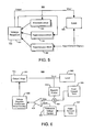
- Figure 1A illustrates an example of a hard disk drive system that can be used with a voltage regulating system of the present invention.
- Figure 1B illustrates a block diagram of a voltage regulating system that is responsive to feed-forward information indicative of deterministic changes in the load current, according to an embodiment of the present invention.
- Figure 1C is a graph that illustrates examples of a read gate signal and a read gate feed-forward signal, according to an embodiment of the present invention.
- Figure 2A illustrates a block diagram of a voltage regulating system that is responsive to feed-forward information from signals indicating two deterministic events that affect the load current, according to another embodiment of the present invention.
- Figure 2B is a graph that illustrates examples of a servo gate signal and a servo gate feed-forward signal, according to an embodiment of the present invention.
- Figure 3 illustrates a block diagram of a voltage regulating system that is responsive to feed-forward information from signals indicating several different deterministic events that affect the load current, according to yet another embodiment of the present invention.
- Figure 4 illustrates a schematic diagram of a switching voltage regulating system that is responsive to feed-forward information indicating deterministic changes in the load current, according to still another embodiment of the present invention.
- Figure 5 illustrates a generalized block diagram of a voltage regulating system that is responsive to internal and external feed-forward information according to yet another embodiment of the present invention.
- Figure 6 illustrates a block diagram of a voltage regulating system that receives multiple feed-forward terms indicating deterministic changes in the load current at separate inputs of a voltage regulator, according to another embodiment of the present invention.
- a voltage regulator provides a regulated output voltage to a load.
- the voltage regulator changes its output current, the output voltage, or both in response to changes in the load current, the load voltage, or both in order to maintain the output voltage at a substantially constant value.
- Changes in the load current can be classified as random or deterministic. Turning of a light switch is an example of a deterministic change. An accurate prediction can be made that a light bulb will draw a predefined amount of current when it is turned on. A voltage regulator that has only feedback control responds the same way to random and deterministic changes in the load current. However, many types of changes in load current are deterministic in nature. These load current changes happen for a specified reason and have a repeatable behavior.
- a hard disk drive (HDD) system 10 contains a rotating spindle motor 30 for turning the hard disk stack 70, a voice-coil motor (VCM) actuator 40 used to position head arms to different tracks on the surface of the stack 70, and a read/write head on each head arm for reading and writing data onto a hard disk.
- a voice-coil motor (VCM) and motor controller chip 20 manages power for performing the electrical-to-mechanical conversions that are needed to rotate the spindle motor and to move the actuator.
- a HDD controller manages all of the operations of HDD system 10.
- the hard disk drive system 10 When the hard disk drive is commanded to read data from a hard disk, the hard disk drive system 10 causes the actuator 40 to position the read/write head over the desired read location. When the read/write head gets to the desired read location, the HDD controller 25 sends a read gate signal to the data channel 50.
- the read gate signal is a request for the data channel to start fetching data from the disk. In response to the read gate signal, the data channel 50 begins to take the actions needed to read the magnetic data on the disk.
- the hard disk drive (HDD) controller 25 asserts a write gate signal to write data onto a hard disk.
- the HDD controller 25 can also assert a servo gate signal to cause the read/write head to read servo information from a hard disk.
- the servo information is position information that helps the actuator position the read/write head over the correct data track.
- a data channel in a hard disk drive draws a predictable amount of electrical current from a voltage regulator in response to read gate, write gate, and servo gate signals.
- a HDD controller sends a read gate signal to the data channel, the data channel subsequently draws a predictable amount of current to analyze the read signal. Also, the amount of current drawn by the data channel in response to a write gate signal or a servo gate signal is repeatable and predictable.
- FIG. 1B illustrates a voltage regulating system 100 according to a first embodiment of the present invention.
- Voltage regulating system 100 includes a voltage regulator 101, a summing node 102, a feed-forward term 103, and one or more feedback terms 104.
- Data channel 105 is the load in the hard disk drive that draws current from the output of the voltage regulator 101.
- Voltage regulator 101 can be a synchronous switching voltage regulator, a non-synchronous switching voltage regulator, a linear voltage regulator, or any other type of voltage regulator. Voltage regulator 101 receives an input voltage V IN and provides an output voltage V OUT at its output to data channel 105. If voltage regulator 101 is a switching regulator, it typically includes an output inductor and an output capacitor for maintaining a continuous output voltage and/or current flow.
- Each feedback term 104 receives a feedback signal from the output of voltage regulator 101.
- the feedback signal can be, for example, a voltage feedback signal that is proportional to the output voltage or a current feedback signal that is indicative of the output current.
- Each feedback term 104 uses the feedback information to generate a control signal.
- the control signal is provided to the voltage regulator at the output stage pass element or switch (transistor base or gate) to control the regulator output current, output voltage, or both.
- a feedback term 104 can include a resistor divider coupled to the regulator output terminal and an input of an error amplifier or comparator.
- the error amplifier amplifies the difference between the voltage feedback signal and a reference voltage to generate an error signal.
- the comparator determines if the error is high or low and outputs a corresponding logical control signal.
- the voltage regulator uses the error signal or the logical control signal to control the duty cycle of an output switching transistor so that the output voltage remains substantially constant.
- Feedback terms 104 can employ any one or more of a variety of feedback control techniques to control the output current in response to a feedback signal.
- feedback terms 104 can include any voltage-mode or current-mode techniques that are well known for use in voltage regulators.
- Voltage regulation system 100 can include multiple feedback terms 104 that are responsive to multiple feedback signals.
- voltage regulation system 100 can be responsive to a voltage feedback signal from the output voltage and a current feedback signal from the output current. Both the current and the voltage feedback signal can be used to generate a combined control signal for the voltage regulator at summing node 102 or at various points within the regulator's control loop.
- Voltage regulator 101 uses the combined control signal to adjust the output current, the output voltage, or both, to maintain a substantially constant output voltage.
- Voltage regulation system 100 also has a feed-forward term 103 that is responsive to a read gate signal.
- Feed-forward term 103 provides a feed-forward signal to voltage regulator 101 in response to an input signal that is generated from a source external to the voltage regulating system and that indicates a deterministic change in the load.
- the input signal is a read gate signal generated from a hard disk drive system.
- Feed-forward term 103 receives the read gate signal and, in response, generates a read gate feed-forward signal as an output.
- the read gate signal is a logic signal.
- the feed-forward term 103 converts the read gate signal into a read gate feed-forward signal.
- a falling edge of the read gate signal indicates the start of a read operation for a sector of data, and a rising edge of the read gate signal indicates the end of a read operation.
- the feed-forward term generates a downward pulse in the read gate feed-forward signal after each falling edge of the read gate signal, and a upward pulse in the read-gate feed-forward signal after each rising edge of the read gate signal.
- Feed-forward term 103 provides the read gate feed-forward signal to voltage regulator 101 at summing node 102.
- the one or more feedback control signals and the read gate feed-forward signal are combined at summing node 102 and provided to the voltage regulator 101, as shown in Figure 1B.
- Voltage regulator 101 uses the combined signal generated at summing node 102 to regulate the output current (and/or other control signals) provided to load 105.
- a change in the read gate signal is indicative of a deterministic change in the load current drawn by data channel 105.
- voltage regulator 101 receives a signal from summing node 102 that is indicative of a read gate function, voltage regulator 101 increases its output current to match the deterministic change that the load current it is about to experience.
- voltage regulator 101 increases its output current by an amount equal to the predicted increase in the data channel load current. After the read gate function is complete, voltage regulator 101 decreases its output current in response to a rising edge in the read gate feed-forward signal by an amount equal to the predicted decrease in the data channel load current.
- the read gate logic signal is inverted in order to create the appropriate signal polarity or phase, to achieve the desired response in the voltage regulator.
- the present invention is advantageous, because it allows voltage regulator 101 to adjust its output to match a deterministic change in the load before V OUT varies significantly.
- Feed-forward term 103 can cause the output current of regulator 101 to match a deterministic change in the load current before feedback terms 104 can respond to the change in V OUT .
- FIG. 2A illustrates a voltage regulating system 200 according to a second embodiment of the present invention.
- System 200 includes all of the elements of system 100 and an additional feed-forward term 201.
- Feed-forward term 201 receives a servo gate signal.
- a servo gate signal is a signal generated by a HDD controller to cause data channel 105 to read a servo track on a hard disk.
- Feed-forward term 201 generates the servo gate feed-forward signal in response to the servo gate signal. Rising and falling pulses in the servo gate feed-forward signal correspond to rising and falling edges, respectively, of the digital servo gate signal.
- the feedback control signals, the read gate feed-forward signal, and the servo gate feed-forward signal from feed-forward term 201 are summed at node 102 and then provided to regulator 101.
- data channel 105 increases its load current by a predictable amount in response to a falling edge in the servo gate signal, which occurs at the start of a servo read operation.
- Data channel 105 increases its load current to perform the servo read operation.
- Data channel 105 decreases its load current by a predictable amount in response to a rising edge in the servo gate signal, which occurs at the termination of the servo read operation.
- data channel 105 increases its load current by a predictable amount during a servo read, and decreases its load current by a predictable amount after the servo read.
- voltage regulator 101 responds to the servo gate signal to adjust its output current to match a predicted change in the load current so that the output voltage remains substantially constant.
- FIG. 3 illustrates a voltage regulating system 300 that is responsive to feed-forward information indicative of deterministic changes in the load current, according to a third embodiment of the present invention.
- Voltage regulating system 300 includes all of the elements of system 100, term selector register 301, variable weighting register 302, summing circuit 303, and hardware/software control unit 304. Voltage regulating system 300 is responsive to feed-forward signals indicative of several different deterministic events that affect the load current at load 105.
- Control unit 304 can be a software-based or hardware-based system. Control unit 304 provides control signals that are indicative of deterministic changes in the load current drawn by load 105. For example, control unit 304 can provide a read gate signal, a servo gate signal, a write gate signal, etc. Control unit 304 stores the current states of these control signals in term selector register 301. For example, each storage unit in register 301 can store one control bit (1 or 0) to indicate the state of each control signal.
- the control bits stored in register 301 are transmitted to variable weighting register 302.
- the control bits are multiplied by one of some number, "n", of weighting coefficients, called A1 through An, respectively, in register 302 to provide a desired weight for each control signal.
- the weighting coefficients are set to values based on a weight to be given to each of the "n" control signals with respect to their desired effect on the output current of regulator 101. For example, the weighting coefficients can be selected to cause the read gate signal to have more of an effect on the output current of regulator 101 than the servo gate signal.
- variable weighting register 302 The outputs of variable weighting register 302 are summed together at summing circuit 303.
- the summed output signal of summing circuit 303 is converted into a feed-forward signal by feed-forward term 103.
- the feed-forward signal is summed with the feedback control signals at summing node 102.
- the summed output signal of node 102 provided to regulator 101 to control the output current.
- FIG. 4 illustrates a schematic diagram of a switching voltage regulating system 400 that is responsive to feed-forward information indicative of deterministic changes in the load current, according to a further embodiment of the present invention.
- Voltage regulating system 400 includes a p-channel switching transistor 401.
- the source of transistor 401 is coupled to receive an input voltage V IN .
- the drain of transistor 401 is coupled to an output inductor 405 and a Schottky diode 417.
- Output inductor 405 is also coupled to an output capacitor 416, which stores charge that is provided to a load.
- the load receives a regulated output voltage V OUT .
- p-channel switching transistor 401 can be replaced an n-channel switching transistor that has corresponding support from drive circuitry 415, a Bipolar junction switching transistor (e.g., NPN or PNP BJT), a pass element, etc.
- Diode 417 can be replaced a second switching transistor that has corresponding support from drive circuitry 415 to allow for synchronous rectification.
- System 400 has a feedback term that is used to regulate the output voltage in response to changes in the output voltage.
- the feedback term is implemented by a feedback loop.
- the feedback loop includes resistors 411-413, amplifier/comparator 410, frequency control 414, and drive circuitry 415.
- Three feedback resistors 411, 412, and 413 form a resistor divider that generate a feedback voltage V FB , which is proportional to the output voltage V OUT .
- a hysteretic comparator 410 compares the feedback voltage to a bandgap reference voltage V BGR to generate a control signal.
- a hysteretic comparator has two threshold voltages that are set based on resistor 412.
- circuit 410 can be an error amplifier 410 that amplifies the difference between the feedback voltage V FB and the bandgap reference voltage V BGR to generate a control signal.
- the control signal is indicative of a deviation in the output voltage V OUT from a target value.
- the control signal from circuit 410 is provided to frequency control circuitry 414.
- Frequency control circuitry 414 generates a duty cycle control signal in response to the control signal from circuit 410.
- the drive circuitry 415 turns switching transistor on and off in response to the duty cycle control signal.
- Frequency control circuitry 414 can regulate the duty cycle of switching transistor 401 using pulse width modulation for a constant switching frequency (e.g., using an error amplifier) or pulse frequency modulation for a variable frequency (e.g., determined by the comparator output signal provided using a hysteretic comparator).
- transistor 401 When switching transistor 401 is on, current flows from V IN through transistor 401 and inductor 405 to the load, and the current in the inductor 405 ramps up. When transistor 401 is off, current flows from ground through the Schottky diode 417 and inductor 405 to the load. Current in inductor 405 ramps down when transistor 401 is off.
- Frequency control circuitry 414 regulates the duty cycle of switching transistor 401 so that the average output current through inductor 405 matches the load current to maintain V OUT at a substantially constant value.
- amplifier/comparator 410 senses a change in the output voltage V OUT , the feedback loop varies the duty cycle of switching transistor 414 so that the average inductor current matches the load current.
- System 400 also includes a feed-forward circuit 402-403 that compensates by deriving a signal from the inductor voltage transient and a feedback capacitor 418 that compensates for changes at the output.
- Feedback capacitor 418 is coupled in parallel with resistor 413 between output capacitor 416 and summing node 102.
- the output voltage ripple causes a current to be sourced through capacitor 418 during each switching cycle.
- Capacitor 418 reduces the sensing impedance to transient signals to reduce the output voltage ripple.
- Capacitor 418 can also increase the operating frequency of the regulator in a variable frequency regulator. Capacitor 418 can cause the control circuitry to respond to changes in the output voltage faster than the resistor divider. However, the feedback path through capacitor 418 requires a change in the output voltage before the regulator can adjust the duty cycle of transistor 401.
- Resistor 402 and capacitor 403 are coupled in series between the drain of transistor 401 and summing node 102 in system 400. Resistor 402 and capacitor 403 are also added to reduce the output voltage ripple by injecting a ramp signal to the feedback voltage at the non-inverting input of comparator 410. For example, comparator 410 causes transistor 401 to turn off in response to the voltage from resistor 402 and capacitor 403 before V OUT has increased to the feedback hysteresis point to help reduce overshoot in V OUT if the load current decreases quickly.
- comparator 410 causes transistor 401 to turn on in response to the decreasing ramp voltage from resistor 402 and capacitor 403 before V OUT has drooped below the hysteresis point, thus reducing undershoot in V OUT if the load current suddenly increases.
- the alternating current through resistor 402 and capacitor 403 also helps to remove the modulating effect that the switching duty cycle of transistor 401 has on the output voltage V OUT as a function of load current.
- the path through resistor 402 and capacitor 403 does not provide a feed-forward term indicative of deterministic changes in the load current.
- Passive components 411-413, 418, 402, and 403, all are tuned to provide a weighted contribution on the value of feedback voltage V FB at the non-inverting input of amplifier/comparator 410. In another embodiment of the invention, this may be an inverting configuration.
- a feed-forward circuit of the present invention provides feed-forward information in voltage regulating system 400 that indicates deterministic changes in the load current.
- the feed-forward circuit includes resistor 408 and capacitor 409.
- Capacitor 409 receives a read gate signal at one of its inputs.
- Capacitor 409 and resistor 408 convert the read gate signal into the read gate feed-forward signal, as shown in Figure 1C.
- Capacitor 409 blocks the DC component of the read gate signal, passing only an AC component of the read gate signal.
- the read gate signal does not affect the output current of the voltage regulator when the read gate signal is in a steady state.
- the feedback loop can effectively regulate the output current in response to random changes in the output voltage.
- Resistor 408 provides a damping factor.
- Resistor 408 and capacitor 409 are merely one example of a feed-forward circuit of the present invention.
- a feed-forward circuit can also be implemented software or in another configuration of hardware components.
- the voltage changes in the read gate feed-forward signal correspond to the edges of the read gate signal. They affect the voltage feedback signal V FB at the beginning and the end of the read operation. As described above, a falling edge of the read gate causes a read operation to begin. Resistor 408 and capacitor 409 generate a falling voltage in the read gate feed-forward signal at summing node 102 in response to a falling edge in the read gate signal. The falling voltage at node 102 causes feedback voltage V FB to decrease, which in turn, causes the feedback loop to increase the on-time of transistor 401, sending more current to the load.
- the feed-forward circuitry allows voltage regulating system 400 to increase its output current to match a deterministic increase in the load current during a read function. By accurately matching the output current and the load current, the present invention prevents the output voltage from dropping below its tolerance range at the start of a read function.
- a rising edge of the read gate signal causes the read function to end.
- Resistor 408 and capacitor 409 generate a rising edge in the read gate feed-forward signal at summing node 102 in response to a rising voltage in the read gate signal.
- the rising voltage at node 102 causes feedback voltage V FB to increase, which in turn, causes the feedback loop to decrease the on-time of transistor 401, sending less output current to the load.
- the feed-forward circuitry allows voltage regulating system 400 to decrease its output current to match a deterministic decrease in the load current after a read function.
- the present invention prevents the output voltage from overshooting its tolerance range after a read function.
- comparator 410 can be implemented entirely on an integrated circuit chip, as discrete components, or as a combination of discrete components and integrated circuit chips.
- comparator 410, frequency control 414 and drive circuitry 415 can be integrated onto a single chip.
- switching transistor 401, output capacitor 416, output inductor 405, resistors 411-413, resistor 402, resistor 408, and capacitors 403, 409, and 418 are all external discrete components.
- the feed-forward circuitry 408 and 409 of Figure 4 can be duplicated to receive additional feed-forward signals. However, if multiple feed-forward signals are provided to a voltage regulator, a solution is required that balances the response to the multiple pathways simultaneously.
- An alternative embodiment buffers the signals from each source such that low impedances can be used to combine (i.e., add or subtract) each contribution without concern for its impact on the other pathways. Then, each individual factor can be weighted independently according to requirements.
- programmable control registers 301 as shown in Figure 3, which eliminate the need for external components to implement the feed-forward terms.
- additional pins are added to a voltage regulator integrated circuit to allow tuning of gains, for example, with a high degree of flexibility.
- a drawback of additional circuitry is potential increases in feedback error (gains and offsets) for the regulator.
- FIG. 5 illustrates a generalized block diagram of a voltage regulating system 500 that is responsive to feed-forward information according to an embodiment of the present invention.
- Voltage regulating system 500 includes a voltage regulator 501, a feedback circuit 502, and feed-forward circuits 503 and 504.
- Voltage regulating system 500 provides output current to a load 505.
- Feedback circuit 502 generates one or more feedback signals from the regulator output.
- Feed-forward circuit 503 generates one or more feed-forward signals from a node that is internal to the regulator.
- Feed-forward circuit 504 generates any number of feed-forward signals responsive to external feed-forward information that indicates deterministic changes in the load current.
- feed-forward circuit 504 can receive one or more signals indicative of deterministic loads and can generate one or more output signals that are used to control an output condition of a voltage regulator.
- Regulating system 500 can include any number of feed forward circuits 504, e.g., one or more feed forward circuits 504 that receive any number of input signals indicative of deterministic loads and generate any number of feed-forward signals for controlling an output condition of a voltage regulator.
- the feedback signals generated by feedback circuit 502, the feed-forward signals generated by feed-forward circuit 503, and the deterministic signals from feed-forward circuit 504 can be provided to separate inputs of voltage regulator 500.
- a feedback signal from feedback circuit 502 and a feed-forward signal from circuit 504 can be provided to separate inputs of voltage regulator 501.
- two feed-forward signals generated by circuit 504 can be provided to separate inputs of voltage regulator 501.
- FIG. 6 illustrates a block diagram of a voltage regulating system 600 that receives multiple feed-forward terms at separate inputs of a voltage regulator.
- Voltage regulating system 600 includes an output stage 601, a resistor divider 603, feed-forward terms 604 and 607, reference voltage control circuit 606, circuit element 605, and voltage regulator control and drive circuitry 608.
- Each of the feed-forward terms 604 and 607 provide signals to regulating system 600 that are indicative of deterministic changes in the load current.
- Output stage 601 includes an output inductor, an output capacitor, and an output transistor, which can be, for example, a pass element or a switching transistor.
- Circuit element 605 can be, for example, a hysteretic comparator or an error amplifier.
- Voltage regulating system 600 provides output current from V IN through output stage 601 to load 602 at V OUT .
- Resistor divider 603 generates a divided down voltage feedback signal V FB at the non-inverting input of amplifier/comparator 605.
- Amplifier/comparator 605 compares the voltage feedback signal to a reference voltage V REF from reference voltage control 606 to generate a control signal.
- Voltage regulator control and drive circuitry 608 uses the control signal to control the amount of current provided to load 602 through output stage 601.
- Feed-forward term 604 can provide a feed-forward signal to a summing node 609 that indicates deterministic changes in the load before the changes are fully reflected in V OUT .
- Resistor 408 and capacitor 409 in Figure 4 are an example of feed-forward term 604.
- the feed-forward signal from term 604 can be a response to a read gate signal, a write gate signal, a servo gate signal, etc.
- Reference voltage control circuit 606 generates a reference voltage V REF that is provided to the inverting input of amplifier/comparator 605.
- Reference voltage control circuit 606 usually provides a constant reference voltage to the inverting input of amplifier comparator 605.
- Feed-forward term 607 can provide a feed-forward signal to reference voltage control 606 that indicates deterministic changes in the load current in load 602 before the changes are reflected in V OUT .
- the feed-forward signal from term 607 can be a response to a read gate signal, a write gate signal, a servo gate signal, etc.
- Control circuit 606 adjusts reference voltage V REF in response to the feed-forward signal from term 607.
- Control circuit 606 can, for example, include a microprocessor that has the capability to trim the reference voltage V REF according to an internal pending load change it is predicting.
- the microprocessor can trim the reference voltage, for example, via a communication bus using reference voltage trimming control registers.
- control circuit 606 When reference voltage control 606 receives a feed-forward signal from term 607 indicating an increase in the expected load current, control circuit 606 increases the reference voltage V REF .
- amplifier/comparator 605 adjusts its output control signal so that output stage 601 provides more output current to load 602. For example, in response to an increased reference voltage, an error amplifier 605 causes its output error signal to decrease so that duty cycle of a switching transistor in output stage 601 increases.
- a comparator 605 causes its output signal to remain low for a longer period of time to increase the duty cycle of a switching transistor in output stage 601.
- control circuit 606 When reference voltage control 606 receives a feed-forward signal from term 607 indicating a decrease in the expected load current, control circuit 606 decreases the reference voltage V REF ⁇ In response to the decreased reference voltage, amplifier/comparator 605 adjusts its output control signal so that output stage 601 provides less output current to load 602.
- Feed-forward information of the present invention can be used in any device with operating modes that have distinct, deterministic load characteristics. Any mode change is very likely to have a predictable corresponding load change. A mode change is triggered by an event either externally (e.g., pushing a button, receiving a call request, etc.) or internally (e.g., placing a call, firmware-triggered event such as sleep mode timeout from inactivity, etc.).
- Cell phones can have events tied to placing and receiving calls, responding to key presses, sending/receiving/displaying data, backlighting, etc.
- DVDs can have display driver events such as enable/disable display, and selective vs. full-rate refresh.
- CDs, DVDs, and hard disk drives (HDDs) have events associated with data access such as read/write, idle, active idle, sleep, etc. Any of these events can correspond to a mode change that is associated with a deterministic change in the load current drawn from a voltage regulator.
- the feed-forward information of the present invention can be used to adjust the output current of a voltage regulator in response to a mode change before the mode change causes a significant deviation in the output voltage.
- the present invention can allow a voltage regulator to maintain the output voltage within a tighter tolerance range.
- the Voice Coil Motor (VCM) current profiles or other data contained in lookup tables in a hard disk drive controller or servo controller can also be used to generate feed-forward control signals according to the present invention.
- VCM Voice Coil Motor
- DRAM or Flash volatile memory
- the onset of these functions can be a trigger for a feed-forward term to cause a voltage regulator to pre-compensate for predicted changes in the load current.
- Some functions may not have any one single logic signal associated with the onset of the function. However, embedded firmware knows when these functions are going to occur and can be programmed to generate predictive control signals to pre-compensate the voltage regulating system for the event that it is about to induce, or the command to which it is about to respond, etc.
Landscapes
- Engineering & Computer Science (AREA)
- Power Engineering (AREA)
- Physics & Mathematics (AREA)
- Electromagnetism (AREA)
- General Physics & Mathematics (AREA)
- Radar, Positioning & Navigation (AREA)
- Automation & Control Theory (AREA)
- Dc-Dc Converters (AREA)
- Control Of Voltage And Current In General (AREA)
Applications Claiming Priority (1)
| Application Number | Priority Date | Filing Date | Title |
|---|---|---|---|
| US11/241,046 US7957847B2 (en) | 2005-09-30 | 2005-09-30 | Voltage regulating systems responsive to feed-forward information from deterministic loads |
Publications (2)
| Publication Number | Publication Date |
|---|---|
| EP1770848A2 true EP1770848A2 (de) | 2007-04-04 |
| EP1770848A3 EP1770848A3 (de) | 2008-04-30 |
Family
ID=37697987
Family Applications (1)
| Application Number | Title | Priority Date | Filing Date |
|---|---|---|---|
| EP06253669A Withdrawn EP1770848A3 (de) | 2005-09-30 | 2006-07-13 | Auf Vorwärtskopplungsinformationen aus deterministischen Lasten ansprechende Spannungsregelungssysteme |
Country Status (6)
| Country | Link |
|---|---|
| US (1) | US7957847B2 (de) |
| EP (1) | EP1770848A3 (de) |
| JP (1) | JP2007104894A (de) |
| KR (1) | KR20070037304A (de) |
| CN (1) | CN100468933C (de) |
| TW (1) | TW200712820A (de) |
Cited By (2)
| Publication number | Priority date | Publication date | Assignee | Title |
|---|---|---|---|---|
| EP2117099A1 (de) * | 2008-05-09 | 2009-11-11 | Research In Motion Limited | System und Verfahren zur dynamischen Leistungsverwaltung einer mobilen Vorrichtung |
| EP2648323A1 (de) * | 2012-04-03 | 2013-10-09 | Nxp B.V. | Schaltnetzteil mit aus Lastsollwert abgeleiteter Vorsteuerung |
Families Citing this family (31)
| Publication number | Priority date | Publication date | Assignee | Title |
|---|---|---|---|---|
| US7816900B2 (en) * | 2006-04-05 | 2010-10-19 | International Rectifier Corporation | Correction circuit for improved load transient response |
| US7908496B2 (en) * | 2007-09-29 | 2011-03-15 | Intel Corporation | Systems and methods for communicating voltage regulation information between a voltage regulator and an integrated circuit |
| US9391544B2 (en) | 2008-11-18 | 2016-07-12 | Stmicroelectronics, Inc. | Asymmetrical driver |
| US8471509B2 (en) * | 2008-12-30 | 2013-06-25 | Stmicroelectronics, Inc. | Management of disk drive during power loss |
| WO2010113223A1 (ja) * | 2009-04-01 | 2010-10-07 | 住友重機械工業株式会社 | ハイブリッド型作業機械 |
| US8147661B2 (en) * | 2009-08-31 | 2012-04-03 | Green On Demand Gmbh | Unit for the electrolysis of water |
| US20130268122A1 (en) * | 2010-05-21 | 2013-10-10 | General Electric Company | Systems, Methods, and Apparatus for Driving Servo Actuators |
| US20120290852A1 (en) * | 2011-05-13 | 2012-11-15 | Dell Products L.P. | System and method for voltage regulator optimization through predictive transient warning |
| CN102955554A (zh) * | 2011-08-18 | 2013-03-06 | 鸿富锦精密工业(深圳)有限公司 | 硬盘电压调节电路 |
| NO334364B1 (no) * | 2012-05-03 | 2014-02-17 | Kongsberg Maritime As | Prediktivt reguleringssystem. |
| US10013003B2 (en) * | 2012-11-16 | 2018-07-03 | Linear Technology Corporation | Feed forward current mode switching regulator with improved transient response |
| JP2014112988A (ja) * | 2012-12-05 | 2014-06-19 | Sanken Electric Co Ltd | スイッチング電源装置 |
| US11557967B2 (en) * | 2013-03-28 | 2023-01-17 | Texas Instruments Incorporated | Voltage regulator with adaptive feed-forward compensation for periodic loads |
| DE112013007055B4 (de) * | 2013-06-28 | 2024-11-07 | Intel Corporation | aSpannungsregler mit einer Mitkopplungs- und Rückkopplungssteuerung |
| CN104079176B (zh) | 2014-06-20 | 2016-11-23 | 华为技术有限公司 | 一种电源管理方法及电源 |
| JP6515570B2 (ja) * | 2015-02-18 | 2019-05-22 | Tdk株式会社 | 制御回路およびスイッチング電源装置 |
| JP6540078B2 (ja) * | 2015-02-18 | 2019-07-10 | Tdk株式会社 | 制御回路およびスイッチング電源装置 |
| CN105577053B (zh) * | 2016-02-01 | 2020-11-17 | 西安智财全技术转移中心有限公司 | 触发器及发电机电压调节器 |
| CN107678480A (zh) * | 2017-11-13 | 2018-02-09 | 常州欣盛微结构电子有限公司 | 一种用于低功耗数字电路的线性电压管理器 |
| US10235987B1 (en) * | 2018-02-23 | 2019-03-19 | GM Global Technology Operations LLC | Method and apparatus that cancel component noise using feedforward information |
| US10355584B1 (en) * | 2018-06-29 | 2019-07-16 | Empower Semiconductor, Inc. | Transient response techniques for voltage regulators |
| CN113228483B (zh) * | 2019-03-13 | 2024-01-19 | 爱德万测试公司 | 电源、自动化测试设备、用于操作电源的方法、用于操作自动化测试设备的方法和使用电压变动补偿机制的计算机程序 |
| CN111596715B (zh) * | 2020-05-29 | 2025-10-31 | 北京集创北方科技股份有限公司 | 电压调整装置、芯片、电源及电子设备 |
| IT202100003368A1 (it) * | 2021-02-15 | 2022-08-15 | St Microelectronics Srl | Circuito di controllo per controllare uno stadio di commutazione di un convertitore elettronico, convertitore elettronico e procedimento corrispondenti |
| KR20220124499A (ko) * | 2021-03-03 | 2022-09-14 | 에스케이하이닉스 주식회사 | 레귤레이터 |
| US12072830B2 (en) * | 2021-11-16 | 2024-08-27 | Infineon Technologies Austria Ag | Flexible high speed interface implementation in a power supply |
| CN114124005B (zh) * | 2021-11-23 | 2024-10-22 | 华中科技大学 | 一种具有前馈型匹配负载的分布式放大器 |
| CN115167592A (zh) * | 2022-06-30 | 2022-10-11 | 超聚变数字技术有限公司 | 一种稳压电路、供电电路及供电控制方法 |
| US12374982B2 (en) * | 2023-03-31 | 2025-07-29 | Novatek Microelectronics Corp. | Feedback control device and feedback control method for DC-to-DC converter |
| CN120949883B (zh) * | 2025-10-17 | 2025-12-23 | 呼伦贝尔学院 | 基于负载电流预测的无线传感器动态电压调节方法及系统 |
| CN121584647B (zh) * | 2026-01-28 | 2026-04-24 | 国网四川省电力公司德阳供电公司 | 一种数字电压补偿方法 |
Family Cites Families (21)
| Publication number | Priority date | Publication date | Assignee | Title |
|---|---|---|---|---|
| US4425612A (en) | 1982-05-12 | 1984-01-10 | International Business Machines Corporation | Power supply with load-transient anticipation |
| US5258903A (en) | 1991-12-16 | 1993-11-02 | Thomson Consumer Electronics | Control circuit and power supply for televisions |
| JP3956057B2 (ja) | 1996-01-31 | 2007-08-08 | エイエスエム アメリカ インコーポレイテッド | 熱処理のモデル規範型予測制御 |
| KR100194027B1 (ko) * | 1996-02-22 | 1999-06-15 | 윤종용 | 섹터 펄스 생성방법과 회로 |
| US5905407A (en) * | 1997-07-30 | 1999-05-18 | Motorola, Inc. | High efficiency power amplifier using combined linear and switching techniques with novel feedback system |
| US6529973B1 (en) * | 2000-05-22 | 2003-03-04 | Adaptec, Inc. | Programmable generic read channel control device |
| US20020071231A1 (en) * | 2000-12-12 | 2002-06-13 | Chloupek James E | Hard disk drive (HDD) electrical over voltage stress (EOS) systems and methods |
| US6593725B1 (en) * | 2001-02-22 | 2003-07-15 | Cypress Semiconductor Corp. | Feed-forward control for DC-DC converters |
| US6639373B2 (en) * | 2001-09-28 | 2003-10-28 | Texas Instruments Incorporated | Driver circuit for a voice coil motor in a disk drive system |
| US6639391B2 (en) | 2002-02-25 | 2003-10-28 | Intel Corporation | Variable switching frequency voltage regulator to optimize power loss |
| EP1367703A1 (de) * | 2002-05-31 | 2003-12-03 | STMicroelectronics S.r.l. | Methode zur Regelung der Versorgungsspannung eines Verbrauchers sowie der dazugehörige Spannungsregler |
| US6724174B1 (en) * | 2002-09-12 | 2004-04-20 | Linear Technology Corp. | Adjustable minimum peak inductor current level for burst mode in current-mode DC-DC regulators |
| US6801027B2 (en) | 2002-09-26 | 2004-10-05 | Itt Manufacturing Enterprises, Inc. | Power conversion in variable load applications |
| US6906502B2 (en) | 2002-11-14 | 2005-06-14 | Fyre Storm, Inc. | Method for regulating an output voltage of a power coverter |
| DE10346965A1 (de) | 2003-10-09 | 2005-06-02 | Siemens Ag | Spannungsregelung für räumlich entfernte Verbraucher |
| US7038435B2 (en) * | 2003-11-24 | 2006-05-02 | Raytheon Company | Method for input current regulation and active-power filter with input voltage feedforward and output load feedforward |
| US7161335B2 (en) | 2004-02-20 | 2007-01-09 | Virginia Tech Intellectual Properties, Inc. | Adaptive bus voltage positioning for two-stage voltage regulators |
| US7298567B2 (en) * | 2004-02-27 | 2007-11-20 | Hitachi Global Storage Technologies Netherlands B.V. | Efficient low dropout linear regulator |
| US7292015B2 (en) * | 2004-11-18 | 2007-11-06 | Matsushita Electric Industrial Co., Ltd. | High efficiency, high slew rate switching regulator/amplifier |
| US7019503B1 (en) | 2005-02-07 | 2006-03-28 | Raytheon Company | Active power filter with input voltage feedforward, output load feedforward, and output voltage feedforward |
| US7441137B1 (en) * | 2005-07-25 | 2008-10-21 | Nvidia Corporation | Voltage regulator with internal controls for adjusting output based on feed-forward load information |
-
2005
- 2005-09-30 US US11/241,046 patent/US7957847B2/en not_active Expired - Fee Related
-
2006
- 2006-07-13 EP EP06253669A patent/EP1770848A3/de not_active Withdrawn
- 2006-07-26 TW TW095127215A patent/TW200712820A/zh unknown
- 2006-08-23 KR KR1020060080112A patent/KR20070037304A/ko not_active Withdrawn
- 2006-08-24 CN CNB2006101214836A patent/CN100468933C/zh not_active Expired - Fee Related
- 2006-09-26 JP JP2006260580A patent/JP2007104894A/ja active Pending
Cited By (7)
| Publication number | Priority date | Publication date | Assignee | Title |
|---|---|---|---|---|
| EP2117099A1 (de) * | 2008-05-09 | 2009-11-11 | Research In Motion Limited | System und Verfahren zur dynamischen Leistungsverwaltung einer mobilen Vorrichtung |
| US8217626B2 (en) | 2008-05-09 | 2012-07-10 | Research In Motion Limited | System and method for dynamic power management of a mobile device |
| EP2262075A3 (de) * | 2008-05-09 | 2013-03-27 | Research In Motion Limited | System und Verfahren zur dynamischen Leistungsverwaltung einer mobilen Vorrichtung |
| US8493029B2 (en) | 2008-05-09 | 2013-07-23 | Research In Motion Limited | System and method for dynamic power management of a mobile device |
| US8760119B2 (en) | 2008-05-09 | 2014-06-24 | Blackberry Limited | System and method for dynamic power management of a mobile device |
| EP2648323A1 (de) * | 2012-04-03 | 2013-10-09 | Nxp B.V. | Schaltnetzteil mit aus Lastsollwert abgeleiteter Vorsteuerung |
| US9041468B2 (en) | 2012-04-03 | 2015-05-26 | Nxp B.V. | Switched-mode power supply and method of operation |
Also Published As
| Publication number | Publication date |
|---|---|
| CN100468933C (zh) | 2009-03-11 |
| KR20070037304A (ko) | 2007-04-04 |
| US7957847B2 (en) | 2011-06-07 |
| EP1770848A3 (de) | 2008-04-30 |
| CN101034848A (zh) | 2007-09-12 |
| JP2007104894A (ja) | 2007-04-19 |
| TW200712820A (en) | 2007-04-01 |
| US20070078568A1 (en) | 2007-04-05 |
Similar Documents
| Publication | Publication Date | Title |
|---|---|---|
| US7957847B2 (en) | Voltage regulating systems responsive to feed-forward information from deterministic loads | |
| US7791324B2 (en) | Switching regulator without a dedicated input current sense element | |
| KR101713359B1 (ko) | Dc-dc 컨버터들과 관련된 향상 | |
| US10211729B2 (en) | Switching regulator having improved transient response and control circuit thereof | |
| EP2901244B1 (de) | Regler mit hysteresesteuerung und niedrigem spannungsverlust | |
| US9362829B2 (en) | Voltage regulation associated with a switching converter and a set of linear regulators | |
| US7688047B2 (en) | Power circuit and method of rising output voltage of power circuit | |
| US7764057B2 (en) | Constant-on-time switching power supply with virtual ripple feedback and related system and method | |
| US20100085024A1 (en) | Power supply controller with different steady state and transient response characteristics | |
| JP7645281B2 (ja) | 電圧調整装置、チップ、電源及び電子機器 | |
| EP4134778A1 (de) | Spannungsregelungsvorrichtung, chip, stromversorgung und elektronische vorrichtung | |
| US20110057635A1 (en) | Switching regulator | |
| US11418118B1 (en) | Regulation loop control for voltage regulation in a switch mode power supply | |
| US20050035748A1 (en) | Selective high-side and low-side current sensing in switching power supplies | |
| CN110677025A (zh) | 调压器的电流限制 | |
| KR20170044342A (ko) | 전압 레귤레이터 및 그의 동작 방법 | |
| JP2020137155A (ja) | 電圧変換回路、制御方法及びプログラム | |
| JP6419024B2 (ja) | 電源回路及び車載用電源システム | |
| US20170310211A1 (en) | Regulator for dc-dc hybrid-mode power regulation | |
| KR102865107B1 (ko) | 메모리 장치의 워드라인 전압 생성기 및 이의 동작 방법 | |
| US9471072B1 (en) | Self-adaptive voltage scaling | |
| Kim et al. | Area-efficient analog peripheral circuit techniques for Solid State Drive with NAND flash memories | |
| JP2020171076A (ja) | 半導体装置 | |
| KR20160002019U (ko) | Uvlo 보호기능이 추가된 ldo 레귤레이터 |
Legal Events
| Date | Code | Title | Description |
|---|---|---|---|
| PUAI | Public reference made under article 153(3) epc to a published international application that has entered the european phase |
Free format text: ORIGINAL CODE: 0009012 |
|
| AK | Designated contracting states |
Kind code of ref document: A2 Designated state(s): AT BE BG CH CY CZ DE DK EE ES FI FR GB GR HU IE IS IT LI LT LU LV MC NL PL PT RO SE SI SK TR |
|
| AX | Request for extension of the european patent |
Extension state: AL BA HR MK YU |
|
| PUAL | Search report despatched |
Free format text: ORIGINAL CODE: 0009013 |
|
| AK | Designated contracting states |
Kind code of ref document: A3 Designated state(s): AT BE BG CH CY CZ DE DK EE ES FI FR GB GR HU IE IS IT LI LT LU LV MC NL PL PT RO SE SI SK TR |
|
| AX | Request for extension of the european patent |
Extension state: AL BA HR MK RS |
|
| 17P | Request for examination filed |
Effective date: 20081006 |
|
| 17Q | First examination report despatched |
Effective date: 20081203 |
|
| AKX | Designation fees paid |
Designated state(s): DE FR GB |
|
| STAA | Information on the status of an ep patent application or granted ep patent |
Free format text: STATUS: THE APPLICATION IS DEEMED TO BE WITHDRAWN |
|
| 18D | Application deemed to be withdrawn |
Effective date: 20090415 |