EP1772732A1 - Réseaux d'électrodes interdigités par réplication de polymères pour des applications de (bio)-détection - Google Patents
Réseaux d'électrodes interdigités par réplication de polymères pour des applications de (bio)-détection Download PDFInfo
- Publication number
- EP1772732A1 EP1772732A1 EP05109353A EP05109353A EP1772732A1 EP 1772732 A1 EP1772732 A1 EP 1772732A1 EP 05109353 A EP05109353 A EP 05109353A EP 05109353 A EP05109353 A EP 05109353A EP 1772732 A1 EP1772732 A1 EP 1772732A1
- Authority
- EP
- European Patent Office
- Prior art keywords
- conductive material
- channels
- sensor according
- electrodes
- zone
- Prior art date
- Legal status (The legal status is an assumption and is not a legal conclusion. Google has not performed a legal analysis and makes no representation as to the accuracy of the status listed.)
- Withdrawn
Links
- 229920000642 polymer Polymers 0.000 title claims abstract description 8
- 238000003491 array Methods 0.000 title abstract description 5
- 239000004020 conductor Substances 0.000 claims abstract description 128
- 238000002955 isolation Methods 0.000 claims abstract description 96
- 230000008021 deposition Effects 0.000 claims abstract description 66
- 238000000034 method Methods 0.000 claims abstract description 46
- 238000004519 manufacturing process Methods 0.000 claims abstract description 28
- 229910052710 silicon Inorganic materials 0.000 claims abstract description 17
- 239000010703 silicon Substances 0.000 claims abstract description 17
- 238000000465 moulding Methods 0.000 claims abstract description 6
- 238000009713 electroplating Methods 0.000 claims abstract description 4
- 238000000151 deposition Methods 0.000 claims description 86
- 239000000758 substrate Substances 0.000 claims description 56
- 239000000463 material Substances 0.000 claims description 37
- 239000000523 sample Substances 0.000 claims description 28
- -1 polybutylene terephthalate Polymers 0.000 claims description 15
- 238000000059 patterning Methods 0.000 claims description 14
- 229920000089 Cyclic olefin copolymer Polymers 0.000 claims description 10
- 229920002492 poly(sulfone) Polymers 0.000 claims description 10
- 238000009739 binding Methods 0.000 claims description 8
- 238000004377 microelectronic Methods 0.000 claims description 7
- 229930040373 Paraformaldehyde Natural products 0.000 claims description 6
- 229920001707 polybutylene terephthalate Polymers 0.000 claims description 6
- 229920006324 polyoxymethylene Polymers 0.000 claims description 6
- 238000000926 separation method Methods 0.000 claims description 6
- 108091034117 Oligonucleotide Proteins 0.000 claims description 5
- 229920000265 Polyparaphenylene Polymers 0.000 claims description 5
- JLCPHMBAVCMARE-UHFFFAOYSA-N [3-[[3-[[3-[[3-[[3-[[3-[[3-[[3-[[3-[[3-[[3-[[5-(2-amino-6-oxo-1H-purin-9-yl)-3-[[3-[[3-[[3-[[3-[[3-[[5-(2-amino-6-oxo-1H-purin-9-yl)-3-[[5-(2-amino-6-oxo-1H-purin-9-yl)-3-hydroxyoxolan-2-yl]methoxy-hydroxyphosphoryl]oxyoxolan-2-yl]methoxy-hydroxyphosphoryl]oxy-5-(5-methyl-2,4-dioxopyrimidin-1-yl)oxolan-2-yl]methoxy-hydroxyphosphoryl]oxy-5-(6-aminopurin-9-yl)oxolan-2-yl]methoxy-hydroxyphosphoryl]oxy-5-(6-aminopurin-9-yl)oxolan-2-yl]methoxy-hydroxyphosphoryl]oxy-5-(6-aminopurin-9-yl)oxolan-2-yl]methoxy-hydroxyphosphoryl]oxy-5-(6-aminopurin-9-yl)oxolan-2-yl]methoxy-hydroxyphosphoryl]oxyoxolan-2-yl]methoxy-hydroxyphosphoryl]oxy-5-(5-methyl-2,4-dioxopyrimidin-1-yl)oxolan-2-yl]methoxy-hydroxyphosphoryl]oxy-5-(4-amino-2-oxopyrimidin-1-yl)oxolan-2-yl]methoxy-hydroxyphosphoryl]oxy-5-(5-methyl-2,4-dioxopyrimidin-1-yl)oxolan-2-yl]methoxy-hydroxyphosphoryl]oxy-5-(5-methyl-2,4-dioxopyrimidin-1-yl)oxolan-2-yl]methoxy-hydroxyphosphoryl]oxy-5-(6-aminopurin-9-yl)oxolan-2-yl]methoxy-hydroxyphosphoryl]oxy-5-(6-aminopurin-9-yl)oxolan-2-yl]methoxy-hydroxyphosphoryl]oxy-5-(4-amino-2-oxopyrimidin-1-yl)oxolan-2-yl]methoxy-hydroxyphosphoryl]oxy-5-(4-amino-2-oxopyrimidin-1-yl)oxolan-2-yl]methoxy-hydroxyphosphoryl]oxy-5-(4-amino-2-oxopyrimidin-1-yl)oxolan-2-yl]methoxy-hydroxyphosphoryl]oxy-5-(6-aminopurin-9-yl)oxolan-2-yl]methoxy-hydroxyphosphoryl]oxy-5-(4-amino-2-oxopyrimidin-1-yl)oxolan-2-yl]methyl [5-(6-aminopurin-9-yl)-2-(hydroxymethyl)oxolan-3-yl] hydrogen phosphate Polymers Cc1cn(C2CC(OP(O)(=O)OCC3OC(CC3OP(O)(=O)OCC3OC(CC3O)n3cnc4c3nc(N)[nH]c4=O)n3cnc4c3nc(N)[nH]c4=O)C(COP(O)(=O)OC3CC(OC3COP(O)(=O)OC3CC(OC3COP(O)(=O)OC3CC(OC3COP(O)(=O)OC3CC(OC3COP(O)(=O)OC3CC(OC3COP(O)(=O)OC3CC(OC3COP(O)(=O)OC3CC(OC3COP(O)(=O)OC3CC(OC3COP(O)(=O)OC3CC(OC3COP(O)(=O)OC3CC(OC3COP(O)(=O)OC3CC(OC3COP(O)(=O)OC3CC(OC3COP(O)(=O)OC3CC(OC3COP(O)(=O)OC3CC(OC3COP(O)(=O)OC3CC(OC3COP(O)(=O)OC3CC(OC3COP(O)(=O)OC3CC(OC3CO)n3cnc4c(N)ncnc34)n3ccc(N)nc3=O)n3cnc4c(N)ncnc34)n3ccc(N)nc3=O)n3ccc(N)nc3=O)n3ccc(N)nc3=O)n3cnc4c(N)ncnc34)n3cnc4c(N)ncnc34)n3cc(C)c(=O)[nH]c3=O)n3cc(C)c(=O)[nH]c3=O)n3ccc(N)nc3=O)n3cc(C)c(=O)[nH]c3=O)n3cnc4c3nc(N)[nH]c4=O)n3cnc4c(N)ncnc34)n3cnc4c(N)ncnc34)n3cnc4c(N)ncnc34)n3cnc4c(N)ncnc34)O2)c(=O)[nH]c1=O JLCPHMBAVCMARE-UHFFFAOYSA-N 0.000 claims description 5
- 239000000427 antigen Substances 0.000 claims description 5
- 102000036639 antigens Human genes 0.000 claims description 5
- 108091007433 antigens Proteins 0.000 claims description 5
- 150000001925 cycloalkenes Chemical class 0.000 claims description 5
- 229910052737 gold Inorganic materials 0.000 claims description 5
- 102000004196 processed proteins & peptides Human genes 0.000 claims description 5
- 108090000765 processed proteins & peptides Proteins 0.000 claims description 5
- 239000012488 sample solution Substances 0.000 claims description 5
- 102000004190 Enzymes Human genes 0.000 claims description 4
- 108090000790 Enzymes Proteins 0.000 claims description 4
- 238000001704 evaporation Methods 0.000 claims description 4
- 230000008020 evaporation Effects 0.000 claims description 4
- 238000005240 physical vapour deposition Methods 0.000 claims description 4
- 229910052782 aluminium Inorganic materials 0.000 claims description 3
- 229910052802 copper Inorganic materials 0.000 claims description 3
- AMGQUBHHOARCQH-UHFFFAOYSA-N indium;oxotin Chemical compound [In].[Sn]=O AMGQUBHHOARCQH-UHFFFAOYSA-N 0.000 claims description 3
- 229910052763 palladium Inorganic materials 0.000 claims description 3
- 229910052697 platinum Inorganic materials 0.000 claims description 3
- 239000004417 polycarbonate Substances 0.000 claims description 3
- 229920000515 polycarbonate Polymers 0.000 claims description 3
- 229910052709 silver Inorganic materials 0.000 claims description 3
- 229910052715 tantalum Inorganic materials 0.000 claims description 3
- 229910052719 titanium Inorganic materials 0.000 claims description 3
- 238000002207 thermal evaporation Methods 0.000 claims description 2
- FGUUSXIOTUKUDN-IBGZPJMESA-N C1(=CC=CC=C1)N1C2=C(NC([C@H](C1)NC=1OC(=NN=1)C1=CC=CC=C1)=O)C=CC=C2 Chemical compound C1(=CC=CC=C1)N1C2=C(NC([C@H](C1)NC=1OC(=NN=1)C1=CC=CC=C1)=O)C=CC=C2 FGUUSXIOTUKUDN-IBGZPJMESA-N 0.000 claims 1
- XUIMIQQOPSSXEZ-UHFFFAOYSA-N Silicon Chemical compound [Si] XUIMIQQOPSSXEZ-UHFFFAOYSA-N 0.000 abstract description 16
- 230000008901 benefit Effects 0.000 abstract description 7
- 238000005516 engineering process Methods 0.000 abstract description 4
- 239000002861 polymer material Substances 0.000 abstract description 2
- 238000009396 hybridization Methods 0.000 abstract 1
- 238000011898 label-free detection Methods 0.000 abstract 1
- 150000007523 nucleic acids Chemical class 0.000 abstract 1
- 102000039446 nucleic acids Human genes 0.000 abstract 1
- 108020004707 nucleic acids Proteins 0.000 abstract 1
- 238000001459 lithography Methods 0.000 description 9
- 238000000276 deep-ultraviolet lithography Methods 0.000 description 6
- 239000004033 plastic Substances 0.000 description 6
- 229920003023 plastic Polymers 0.000 description 6
- 239000010931 gold Substances 0.000 description 5
- 230000004044 response Effects 0.000 description 5
- 230000008859 change Effects 0.000 description 4
- 230000008878 coupling Effects 0.000 description 4
- 238000010168 coupling process Methods 0.000 description 4
- 238000005859 coupling reaction Methods 0.000 description 4
- 230000005684 electric field Effects 0.000 description 4
- 239000010408 film Substances 0.000 description 4
- 230000001965 increasing effect Effects 0.000 description 4
- 238000001465 metallisation Methods 0.000 description 4
- 238000012545 processing Methods 0.000 description 4
- VYPSYNLAJGMNEJ-UHFFFAOYSA-N Silicium dioxide Chemical compound O=[Si]=O VYPSYNLAJGMNEJ-UHFFFAOYSA-N 0.000 description 3
- 238000013459 approach Methods 0.000 description 3
- 230000001419 dependent effect Effects 0.000 description 3
- 238000001053 micromoulding Methods 0.000 description 3
- 239000000126 substance Substances 0.000 description 3
- PBCFLUZVCVVTBY-UHFFFAOYSA-N tantalum pentoxide Inorganic materials O=[Ta](=O)O[Ta](=O)=O PBCFLUZVCVVTBY-UHFFFAOYSA-N 0.000 description 3
- PXHVJJICTQNCMI-UHFFFAOYSA-N Nickel Chemical compound [Ni] PXHVJJICTQNCMI-UHFFFAOYSA-N 0.000 description 2
- 239000004952 Polyamide Substances 0.000 description 2
- 230000015572 biosynthetic process Effects 0.000 description 2
- 238000001514 detection method Methods 0.000 description 2
- 230000000694 effects Effects 0.000 description 2
- 238000007667 floating Methods 0.000 description 2
- 239000012634 fragment Substances 0.000 description 2
- PCHJSUWPFVWCPO-UHFFFAOYSA-N gold Chemical compound [Au] PCHJSUWPFVWCPO-UHFFFAOYSA-N 0.000 description 2
- 238000005259 measurement Methods 0.000 description 2
- 238000012544 monitoring process Methods 0.000 description 2
- 230000003287 optical effect Effects 0.000 description 2
- 238000000206 photolithography Methods 0.000 description 2
- 229920003229 poly(methyl methacrylate) Polymers 0.000 description 2
- 229920002647 polyamide Polymers 0.000 description 2
- 239000004926 polymethyl methacrylate Substances 0.000 description 2
- 230000035945 sensitivity Effects 0.000 description 2
- 239000010409 thin film Substances 0.000 description 2
- 239000004642 Polyimide Substances 0.000 description 1
- 229910052581 Si3N4 Inorganic materials 0.000 description 1
- 238000001015 X-ray lithography Methods 0.000 description 1
- PNEYBMLMFCGWSK-UHFFFAOYSA-N aluminium oxide Inorganic materials [O-2].[O-2].[O-2].[Al+3].[Al+3] PNEYBMLMFCGWSK-UHFFFAOYSA-N 0.000 description 1
- 238000004458 analytical method Methods 0.000 description 1
- 238000006243 chemical reaction Methods 0.000 description 1
- 229910052681 coesite Inorganic materials 0.000 description 1
- 230000003750 conditioning effect Effects 0.000 description 1
- 229910052593 corundum Inorganic materials 0.000 description 1
- 229910052906 cristobalite Inorganic materials 0.000 description 1
- 238000005137 deposition process Methods 0.000 description 1
- 238000013461 design Methods 0.000 description 1
- 238000001312 dry etching Methods 0.000 description 1
- 238000000609 electron-beam lithography Methods 0.000 description 1
- 238000004049 embossing Methods 0.000 description 1
- 230000002708 enhancing effect Effects 0.000 description 1
- 238000005530 etching Methods 0.000 description 1
- 239000011521 glass Substances 0.000 description 1
- 238000002347 injection Methods 0.000 description 1
- 239000007924 injection Substances 0.000 description 1
- 238000001746 injection moulding Methods 0.000 description 1
- 239000011810 insulating material Substances 0.000 description 1
- 238000009413 insulation Methods 0.000 description 1
- 239000012212 insulator Substances 0.000 description 1
- 238000004518 low pressure chemical vapour deposition Methods 0.000 description 1
- 150000002734 metacrylic acid derivatives Chemical class 0.000 description 1
- 229910052759 nickel Inorganic materials 0.000 description 1
- 238000000623 plasma-assisted chemical vapour deposition Methods 0.000 description 1
- 238000005498 polishing Methods 0.000 description 1
- 229920001721 polyimide Polymers 0.000 description 1
- 229920001296 polysiloxane Polymers 0.000 description 1
- 230000008569 process Effects 0.000 description 1
- 102000004169 proteins and genes Human genes 0.000 description 1
- 108090000623 proteins and genes Proteins 0.000 description 1
- 239000010453 quartz Substances 0.000 description 1
- 238000010107 reaction injection moulding Methods 0.000 description 1
- 230000009467 reduction Effects 0.000 description 1
- 230000010076 replication Effects 0.000 description 1
- 239000011347 resin Substances 0.000 description 1
- 229920005989 resin Polymers 0.000 description 1
- 150000003839 salts Chemical class 0.000 description 1
- 238000001878 scanning electron micrograph Methods 0.000 description 1
- 239000000377 silicon dioxide Substances 0.000 description 1
- 229910052682 stishovite Inorganic materials 0.000 description 1
- 229920001169 thermoplastic Polymers 0.000 description 1
- 229910052905 tridymite Inorganic materials 0.000 description 1
- 238000001039 wet etching Methods 0.000 description 1
- 229910001845 yogo sapphire Inorganic materials 0.000 description 1
Images









Classifications
-
- C—CHEMISTRY; METALLURGY
- C12—BIOCHEMISTRY; BEER; SPIRITS; WINE; VINEGAR; MICROBIOLOGY; ENZYMOLOGY; MUTATION OR GENETIC ENGINEERING
- C12Q—MEASURING OR TESTING PROCESSES INVOLVING ENZYMES, NUCLEIC ACIDS OR MICROORGANISMS; COMPOSITIONS OR TEST PAPERS THEREFOR; PROCESSES OF PREPARING SUCH COMPOSITIONS; CONDITION-RESPONSIVE CONTROL IN MICROBIOLOGICAL OR ENZYMOLOGICAL PROCESSES
- C12Q1/00—Measuring or testing processes involving enzymes, nucleic acids or microorganisms; Compositions therefor; Processes of preparing such compositions
- C12Q1/001—Enzyme electrodes
-
- G—PHYSICS
- G01—MEASURING; TESTING
- G01N—INVESTIGATING OR ANALYSING MATERIALS BY DETERMINING THEIR CHEMICAL OR PHYSICAL PROPERTIES
- G01N27/00—Investigating or analysing materials by the use of electric, electrochemical, or magnetic means
- G01N27/02—Investigating or analysing materials by the use of electric, electrochemical, or magnetic means by investigating impedance
- G01N27/021—Investigating or analysing materials by the use of electric, electrochemical, or magnetic means by investigating impedance before and after chemical transformation of the material
-
- G—PHYSICS
- G01—MEASURING; TESTING
- G01N—INVESTIGATING OR ANALYSING MATERIALS BY DETERMINING THEIR CHEMICAL OR PHYSICAL PROPERTIES
- G01N33/00—Investigating or analysing materials by specific methods not covered by groups G01N1/00 - G01N31/00
- G01N33/48—Biological material, e.g. blood, urine; Haemocytometers
- G01N33/50—Chemical analysis of biological material, e.g. blood, urine; Testing involving biospecific ligand binding methods; Immunological testing
- G01N33/53—Immunoassay; Biospecific binding assay; Materials therefor
- G01N33/543—Immunoassay; Biospecific binding assay; Materials therefor with an insoluble carrier for immobilising immunochemicals
- G01N33/54366—Apparatus specially adapted for solid-phase testing
- G01N33/54373—Apparatus specially adapted for solid-phase testing involving physiochemical end-point determination, e.g. wave-guides, FETS, gratings
- G01N33/5438—Electrodes
-
- Y—GENERAL TAGGING OF NEW TECHNOLOGICAL DEVELOPMENTS; GENERAL TAGGING OF CROSS-SECTIONAL TECHNOLOGIES SPANNING OVER SEVERAL SECTIONS OF THE IPC; TECHNICAL SUBJECTS COVERED BY FORMER USPC CROSS-REFERENCE ART COLLECTIONS [XRACs] AND DIGESTS
- Y10—TECHNICAL SUBJECTS COVERED BY FORMER USPC
- Y10T—TECHNICAL SUBJECTS COVERED BY FORMER US CLASSIFICATION
- Y10T29/00—Metal working
- Y10T29/49—Method of mechanical manufacture
-
- Y—GENERAL TAGGING OF NEW TECHNOLOGICAL DEVELOPMENTS; GENERAL TAGGING OF CROSS-SECTIONAL TECHNOLOGIES SPANNING OVER SEVERAL SECTIONS OF THE IPC; TECHNICAL SUBJECTS COVERED BY FORMER USPC CROSS-REFERENCE ART COLLECTIONS [XRACs] AND DIGESTS
- Y10—TECHNICAL SUBJECTS COVERED BY FORMER USPC
- Y10T—TECHNICAL SUBJECTS COVERED BY FORMER US CLASSIFICATION
- Y10T29/00—Metal working
- Y10T29/49—Method of mechanical manufacture
- Y10T29/49002—Electrical device making
-
- Y—GENERAL TAGGING OF NEW TECHNOLOGICAL DEVELOPMENTS; GENERAL TAGGING OF CROSS-SECTIONAL TECHNOLOGIES SPANNING OVER SEVERAL SECTIONS OF THE IPC; TECHNICAL SUBJECTS COVERED BY FORMER USPC CROSS-REFERENCE ART COLLECTIONS [XRACs] AND DIGESTS
- Y10—TECHNICAL SUBJECTS COVERED BY FORMER USPC
- Y10T—TECHNICAL SUBJECTS COVERED BY FORMER US CLASSIFICATION
- Y10T29/00—Metal working
- Y10T29/49—Method of mechanical manufacture
- Y10T29/49002—Electrical device making
- Y10T29/49117—Conductor or circuit manufacturing
- Y10T29/49124—On flat or curved insulated base, e.g., printed circuit, etc.
- Y10T29/49155—Manufacturing circuit on or in base
Definitions
- the present invention relates to the field of biosensors.
- the system according to the invention comprises an improved sensor comprising interdigitated electrodes for electronically detecting a binding reaction between molecules or between a pair of chemical substances.
- the present invention further comprises a new cost-effective fabrication method to produce this improved sensor.
- the (bio)sensor system may be used in the field of diagnostics in medical and non-medical applications.
- EP 0 876 601 An insulating substrate is patterned with a plurality of interspaced channels with submicron dimensions. Hills are located on this insulating substrate near the channels such that shadow zones are obtained upon non-orthogonal directional deposition of a conducting material thereby forming an impedimetric device.
- P. Van Gerwen et al propose an optimised design for this sensor, i.e. the hills are located at the end of the channels forming a shadow zone reaching part of the subsequent channel. This avoids electrical contact between adjacent electrode fingers and ensures the formation of interdigitated electrodes.
- a method to produce a sensor comprising at least 2 interdigitated electrodes comprises the following steps:
- forming these isolation structures comprises forming a plurality of interspaced channels and/or hills along opposite sides of at least one of these electrodes.
- the dimensions and locations of these channels and/or hills is chosen such that shadow zones are created at the opposite side of the direction of the beam, such that the interdigitated electrodes are electrically isolated.
- forming these isolation structures consist comprises the steps of
- forming this isolation region further comprises the step of limiting the area wherein said conductive material is deposited such that said isolation structures extend beyond said area at least on the side of the first zone.
- the conductive material connecting the fingers in at least this first zone is limited to a certain area that can be used for contacting this electrode with probes.
- the size of the contacting area can be tuned by properly defining the area where the conductive material is located in combination with the dimensions of the three-dimensional isolation structures.
- the particular shape of the hills in another embodiment reduces the amount of material deposited at the sidewalls of said hills, that way reducing the risk of shorts between the electrode fingers. More specific locations, shapes, numbers, and dimensions for these interspaced channels and/or hills in the isolation region are discussed in the detailed description.
- forming the interdigitated electrodes in the electrode region consists of forming a plurality of interspaced channels and/or hills in the intermediate zone. The dimensions and locations of these channels and/or hills are chosen such that a shadow zone is created at the opposite side of the direction of the beam, such that the fingers of the interdigitated electrodes are electrically isolated.
- the interdigitated electrodes in the electrode region can be produced by any method known in the art, but the method for forming the isolation structures by a combination of appropriate three-dimensional structures in an insulating substrate and a single and directional deposition of conductive material is especially cost-effective when interdigitated electrodes are also produced by the same method. In that case the patterning of three-dimensional structures for creating the interdigitated electrodes and the patterning for creating the isolation structures can be done in one single step, as well as the directional deposition of the conducting material on both the electrode region and isolation region.
- forming the interdigitated electrodes in the electrode region comprises
- the insulating substrate including three-dimensional structures are polymer replicas formed by moulding using mould inserts. These mould inserts are manufactured by electroplating thereby forming a reverse copy of a master structure.
- a master structure can be made of silicon using micro-electronics patterning techniques. Possible materials for the insulating substrate are discussed in the detailed description.
- a sensor comprising at least 2 interdigitated electrodes.
- This sensor is produced by non-orthogonal directional deposition of a conductive material on an insulating substrate, so shows the same advantages as have been set out above with respect to the method, and comprises
- these three-dimensional isolation structures comprise a plurality of interspaced channels and/or hills located along opposite sides of at least one of these electrodes, these channels and/or hills being located and having predetermined dimensions sufficient for maintaining electrical isolation between the interdigitated electrodes upon directional depositing the conductive material.
- the conductive material is located in a limited area such that said isolation structures extend beyond said area at least on the side of the first zone
- the interdigitated electrodes consists of a plurality of interspaced channels and/or hills. On part of these channels and/or hills a conducting layer is located such that the two electrodes of the interdigitated electrode are electrically isolated The dimensions and locations of these channels and/or hills are chosen such that a shadow zone is created at the opposite side of the direction where the beam comes from, such that electrical isolation between the two electrodes of the interdigitated electrode is obtained.
- the electrode region comprises a plurality of second interspaced channels and/or hills in the intermediate zone being located and having dimensions sufficient for maintaining electrical isolation between the fingers of the interdigitated electrodes upon directional depositing the conductive material.
- the insulating substrate including three-dimensional structures is made of a polymer material. Possible materials for the insulating substrate are disclosed.
- an interdigitated electrode array comprising a plurality of electrode regions, having first electrodes electrically isolated from each other by isolation structures and at least part of the second electrodes electrically connected.
- these electrodes are arranged in a geometric array of a predefined number of rows and columns. These columns are electrically isolated from each other by regions where no conducting material is deposited. The isolation regions extend alongside the first electrodes into these regions without conducting material, thereby electrically isolating the first electrodes within each column and electrically connecting the second electrodes of each column.
- a sensor apparatus comprising
- probes for binding to molecules, present in a sample to be tested can be immobilized onto the individual sensors. These probes can be applied to either the insulating part of the channels and/or to the surface of the electrodes.
- top, bottom, over, under and the like in the description and the claims are used for descriptive purposes and not necessarily for describing relative positions. The terms so used are interchangeable under appropriate circumstances and that the embodiments of the invention described herein can operate in other orientations than described or illustrated herein.
- a method to produce a sensor comprising interdigitated electrodes is described.
- the method is based on a combination of appropriate three-dimensional structures in an insulating substrate and a single and directional deposition of conductive material.
- the interdigitated electrode regions need to be complemented with specific features on the three-dimensional structures. Combined with the use of e.g. shadow masks in the deposition step, these features allow for the site-specific deposition of the conductive material.
- the technology described has the additional advantage to integrate highly miniaturized and arrayed electronics elements into polymer micro-fluidics technology, which leads to the affordable manufacturing of (bio)sensor arrays.
- a sensor comprising interdigitated electrodes.
- the sensor of the present invention comprises an insulating layer with conducting interdigitated electrodes on the top.
- the insulating substrate comprised three-dimensional structures.
- These interdigitated electrodes comprise 2 electrodes having a plurality of fingers.
- the fingers of the two electrodes are arranged in an interdigitated way, as illustrated in Figure 1.
- the region where these electrodes are located is called "electrode region”.
- the conductive layers are arranged in a specific geometry thereby enhancing the detection sensitivity of the sensor.
- interdigitated electrodes are formed on an insulating substrate. They comprise two electrodes (see Figure 1) called first electrode (1) and second electrode (2). In principle these interdigitated electrodes can be created by any method known in the art.
- a conducting layer can be deposited on an insulating substrate, followed by lithography and wet and/or dry etching. For patterning interdigitated electrodes lift-off techniques can be used.
- these interdigitated electrodes are preferably produced along with the isolation by a method based on a combination of appropriate three-dimensional structures in an insulating substrate and a single, directional deposition of conductive material.
- the interdigitated electrode regions need to be complemented with specific features on the three-dimensional structure. Combined with a method to limit the conductive material to a limited region, these features allow for the site-specific location of the conductive material.
- these three-dimensional structures consist of a plurality of interspaced channels and/or hills. These channels and/or hills are located and have dimensions such that the shadow zones, created by directional deposition of the conductive material, result in electrical isolation between both electrodes.
- a plurality of interspaced channels and/or hills is created in the insulating substrate.
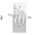
- the base structure is shown in Figure 2, at the left side.
- the structure shows 2 functional elements: channels (3) and hills (4).
- the channels are below the base plane and the hills are elevated above the base plane.
- the interditated electrodes (1) and (2) are realized with a directional deposition process of a conductive material.
- the direction in which this conductive material is deposited is indicated with an arrow in Figure 2.
- Interspaced channels are created within the sensor area in the insulating substrate having essentially the same direction.
- the backside, from a viewpoint of the evaporation direction, of the channels as well as part of the bottom of the channels is shadowed from the evaporated material (see Figure 2, right).
- the channels provide a separation between the adjacent electrode fingers. That way, the channels provide electrical isolation between the interdigitated fingers.
- the exact area of the bottom of the channel that is shadowed from the evaporated material depends on the exact angle of deposition.
- the channels have dimensions such that conductive material at opposite sides of the channels is electrically isolated. Hills are formed at alternating ends of these channels ( Figure 2, left).
- the function of the hills is to create electrical isolation at the outer parts of the electrode fingers.
- a shadow zone is created shadowing part of the base plane in between two channels and the end of the subsequent channel ( Figure 2, right), thereby electrically isolating the end of the fingers of each of the first electrode from the second electrode.
- FIG 3 a topview picture of this embodiment is shown. In the remaining of the detailed description, mainly topview pictures will be used to illustrate different embodiments. In these pictures, the direction in which this conductive material is deposited is indicated with an arrow. Electrode 1 is indicted with (1), electrode 2 with (2), hills with (3), and channels with (4).
- the number of channels in the electrode region is at least more than 4, or even better more than 10, or in between 10 and 100, or in between 10 and 500, preferably between 50 and 500, eventually more than 500.
- the number of channels is chosen such that statistically relevant data are obtained. This means that enough binding should occur in the electrode region.
- contacting the electrode is done in the region connecting the fingers of both electrodes. This region needs to be large enough to allow contacting the regions with external probes. Enlarging the area can be achieved by increasing the number of fingers of the electrodes.
- the width of the electrode fingers and the spacing between the fingers of different electrodes are chosen depending on the dimensions of the molecular structure to be detected.
- the spacing between the fingers of the interdigitated electrodes is chosen comparable to the dimensions of the molecular structure that needs to be detected.
- the distance between the fingers of the interdigitated electrodes depends on the width and depth of the channels and the angle at which the conducting material is deposited. This means that the width and depth of the channels is chosen depending on the molecular structure that needs to be detected, in combination with the deposition angle of the conductive material.
- the interspaced channels both in the electrode region and at the edges of the electrode region have a height and a width in the same order of magnitude.
- the height and the width may be exactly the same for all channels or may vary from one channel to the other.
- the height and the width are preferably chosen between 10 nm and 10 ⁇ m, or between 250 nm and 5 ⁇ m, preferably between 1 ⁇ m and 5 ⁇ m.
- the conductive material needs to be electrically isolated from conductive material surrounding the electrode region. More particular, the conducting material of the top finger and of the bottom finger of the interdigitated electrodes needs to be isolated from surrounding conductive material in order to avoid electrical contact between the two electrodes. Furthermore the size of the conducting area connecting the fingers of the individual electrodes needs to allow contacting the electrodes. The area near the sensor region where the isolation is created is called "isolation region".
- Limiting the material may be done by any method known in the art.
- the conducting material may be deposited through a shadow mask. This is indeed a good method to limit the conducting material connecting the fingers, as this is referred to as a large area.
- a shadow mask is used for locally depositing said conductive material on the patterned substrate.
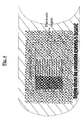
- a method is developed based on a combination of appropriate three-dimensional structures in the insulating substrate located near the electrode region, at least partially outside the electrode region, within the isolation region (see Figure 4) and a single and directional deposition of conductive material. After creating three-dimensional structures a conductive material is deposited in a non-orthogonal direction onto the substrate.
- the angle of deposition is chosen such that these three-dimensional structures create a shadow zone at the opposite side of the direction of the beam thereby creating electrical isolation between these interdigitated electrodes.
- the method is especially cost-effective when interdigitated electrodes are made by the method described above using a combination of an appropriate three-dimensional structure in the same insulating substrate and a single and directional deposition of conductive material.
- the patterning of three-dimensional structures for creating the interdigitated electrodes and the patterning for creating three-dimensional structures for electrically isolating the conducting material within a certain region from other regions can be done in one single step.
- the directional deposition of the conducting material can be done in one step, both in the electrode region and in the isolation region thereby limiting the conductive material to certain well-defined areas.
- these three-dimensional structures in the insulation region are composed of a plurality of interspaced channels and/or hills.
- This can be only channels, only hills, or a combination of channels and hills.
- These channels and/or hills can be parallel to each other or not parallel to each other.
- All hills can have different dimensions or the same dimensions, i.e. width, length, and height in case of hills.
- All channels can have different dimensions or the same dimensions, i.e. width, length, and depth for channels.
- the dimensions and locations of these channels and hills are chosen such that a shadow zone is created at the backside of the hills or in the channels, where essentially no material is deposited, such that the electrodes are electrically isolated.
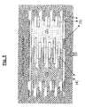
- An example with a possible location of hills (3) and channels (4) can be found in Figure 5.
- the conductive material covers only part of the substrate, including the electrode region.
- Limiting the conductive material to a limited region on the insulating substrate can be done by any method known in the art. This can be achieved by locally depositing said conducting material, for example by using a shadow mask.
- the conducting material is deposited on the complete substrate surface and removed for example by micro-electronics patterning techniques, lithography, lift-off, dry etch, wet etch, or their combination, or any other method known in the art to locally remove locally the conducting material.
- the three-dimensional structures in the isolation region consisting of channels and/or hills at opposite sides of at least one electrode are extending the region wherein the conducting material is located, thereby creating electrically isolated electrodes. An example of locations of hills (3) and channels (4) can be found in Figure 6.
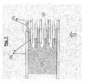
- the hills and channels composing the three-dimensional structures in the isolation region are located at opposite sides of at least one of said electrodes. At one edge the channels are extending outside the region where conductive material is located; the other edge is located near the electrode region. At this edge near the electrode region, hills are located, thereby creating electrodes electrically isolated from each other. Examples of possible arrangements of channels (4) and hills (3) can be found in Figures 7, 8, 9, and 10. The hills can have the same width as the corresponding channels or they can have a different width.
- the width, length, and height of the hills is chosen such that the shadow zone created at the back side of the hill during directional deposition covers at least one edge of the subsequent channel and part of the top of the hill of the subsequent channel.
- the subsequent channel is the channel at the backside of said channel when looking from direction of the beam. That way the material in between those channels is floating.
- the advantage is that the conductive material connecting the fingers of the first electrode is separated from the conductive material connecting the fingers of the second electrode by this plurality of interspaced channels. That way a physical distance between these materials is increased such that coupling between the materials connecting the fingers is minimized and the impedance measured between the electrodes is mainly influenced by a change in the impedance between the electrode fingers.
- the number of channels located in the isolation region is at least more than 2, or more than 10, or in between 10 and 100, or in between 10 and 500, preferably between 100 and 500, or more than 500.
- the choice of the number of the channels is important in case the conducting material in between the channels is floating in order to minimize coupling between the materials connecting the fingers of the electrodes. Furthermore, increasing the area where the conductive material is located, in combination with longer channels, increases the area connecting the electrode fingers, making contacting with probes easier.
- the hills in the isolation region are created such that the edges are tapered (see Figures 8, 9, and 10): that way each hill creates a shadow zone at the backside of the hill during directional deposition covering the tapered edge of the hill of the subsequent channel.
- the subsequent channel or hill is the channel or hill at the backside of said channel when looking from the direction of the beam.
- tapered edges means that the same edge, always left or always right, of the subsequent hill is located behind the previous hill when looking from the direction of the beam.
- the top surface of the hills may have any shape. At least one edge of the hill needs to be free of conducting material to avoid electrical contact between the conducting materials of the different electrodes.
- the hills are made with a top surface having a trapezoidal shape.
- a trapezoid is a 2-dimensional surface having 2 parallel sides of different length. The lines connecting those parallel edges make an angle below 90° with the longest of these parallel sides and an angle larger than 90° with the shortest of these parallel sides.
- the parallel sides are parallel to the direction of the channels, whereby the shortest of these parallel sides is located at the backside when looking from the direction of the beam. Examples of trapezoidal shape are represented in Figure 11.
- any conducting material can be used for the directional deposition. Frequently used materials, presented in an embodiment, are Au, Ag, Pt, Pd, Cu, Al, Ta, Ti, and Indium Tin oxide (ITO).
- the conductive layer can be a thin film. At least all material within one electrode needs to be connected to each other. In the best case, the conducting layer is a uniform continuous thin film. The thickness of the film is at least 5nm, even better between 25nm and 500nm, preferably between 100nm and250nm.
- deposition methods are represented for depositing said conducting layer, i.e. physical vapour deposition (PVD), self-ionised plasma (SIP) deposition, e-beam evaporation, and thermal evaporation.
- PVD physical vapour deposition
- SIP self-ionised plasma
- angles for the directional deposition are selected.
- the angle is below 90° with respect to the normal to the substrate, better between 30° and 89°, preferably between 60° and 85° with respect to the normal on the insulating substrate.
- the angle is chosen such that the shadowing effect of the hills and the channels creates electrical isolation between the interdigitated electrodes. Furthermore, this angle is chosen such that the distance between the fingers of the electrodes matches with the envisaged molecules.
- the insulating substrate can comprise three-dimensional registering features, such as positioning cones or grooves, which can be used for physical referencing in subsequent processing steps.
- the three-dimensional structures in the insulating substrate can be made by any method known in the art. It can be made by microelectronics patterning techniques, using known lithography techniques, e.g. photolithography, preferably UV lithography, even more preferably deep UV lithography, followed by a selective etching. In that case all process steps need to be repeated for every single substrate.
- lithography techniques e.g. photolithography, preferably UV lithography, even more preferably deep UV lithography, followed by a selective etching. In that case all process steps need to be repeated for every single substrate.
- the insulating substrate including the three-dimensional structures can be replicas formed by (injection) moulding, using negative mould inserts or any other method, know in the art, to make replicas.
- the mould inserts can be re-used as a tool for further replication processes. After hardening in the mould inserts, the mould materials have reached a sufficient strength and the separation of mould and mould insert can take place.
- the extremely low roughness of the walls of the mould inserts is most important.
- Such mould inserts can be made with LIGA using X-ray or photolithography, preferably UV lithography, more preferably deep UV lithography, which allows to achieve very small dimensions.
- the mould inserts can also be manufactured by electroplating as a reverse copy of a master structure.
- the mould inserts can be made out of nickel.
- the master structure is made of a silicon master structure using microelectronics patterning techniques. In more detail the following steps can be used. Channels are patterned with a resist layer and dry-etched in bare silicon. A stack of materials for forming the hills is deposited. Any material having a planarizing effect can be used. Chemical mechanical polishing is used to further planarize this stack to allow high-resolution lithography for patterning the hills. Finally the hills are dry-etched into this stack. This results in a positive copy of the insulating substrate.
- This insulating substrate can be made out of an insulating material or can be any material having an insulating top surface.
- An insulating layer formed on the substrate can be a polymer layer such as polyimide or BCB, can be a dielectric or insulating layer such as Si 3 N 4 being deposited by LPCVD or PECVD techniques or SiO 2 deposited or thermally grown on another material.
- An insulating substrate including the three-dimensional structures can be made of a cristallyne material such as quartz or silicon, or an amorphous material such as a glass wafer, or a thick film substrate, such as Al 2 O 3 or can be a polymer.
- Cheap plastic base materials can be produced by injection moulding or hot embossing once a negative master is produced.
- materials used for micro-replication include low viscosity thermoplastic polymers like polymethyl methacrylate (PMMA), polysulfon (PSU), polybutylene terephthalate (PBT), cyclo olefin copolymer (COC), polyoxymethylene (POM), polyphenylene (PPS), polyamide (PA), or polycarbonate (PC), as well as reaction resins based on methacrylates, silicones and caprolactames.
- PMMA polymethyl methacrylate
- PSU polysulfon
- PBT polybutylene terephthalate
- COC cyclo olefin copolymer
- POM polyoxymethylene
- PPS polyphenylene
- PA polyamide
- PC polycarbonate
- said sensor comprises probes for binding to molecules present in a sample to be tested.
- These probes can be applied to either the insulating part of the channels and/or to the surface of the electrodes.
- These probes can be peptides, enzymes, antigens, antibodies, oligonucleotides, DNA or RNA fragments, said probes being covalently or non-covalently attached to said sensor.
- indifferent probes or non-specific conditioning molecules can be applied to either the insulating part of the channels and/or to the surface of electrodes in such a way that this structure effectively acts as a reference structure for back-ground monitoring.
- At least one of the electrodes can be provided with a material of known temperature behaviour for monitoring the temperature behaviour during operation.
- an interdigitated electrode array is presented. It comprises a plurality of electrode regions, electrically isolated from each other by isolation structures as described in the second aspect of the invention.
- the first electrodes of each sensor are electrically isolated and at least part of the second electrodes is electrically connected.
- the individual sensors are arranged in a geometric array in a number of rows and columns.
- the arrangement of the electrodes in this specific array is represented in Figure 12.
- the direction of the channels in the individual sensors is essentially parallel to each other.
- the channels are parallel to the rows of these sensors.
- the conducting material is located in columns covering the electrode regions of the sensors of that row. At one side the conducting material extends the electrode region and the isolation region, thereby electrically connecting one electrode of each sensor in that column. At the other side the channels of the isolation region extend the region where the conductive material is located. That way the first electrode of each sensor is electrically isolated from the other electrodes.
- the advantage is that the impedance of the individual sensors can be measured with a limited number of contacts.
- the channels have a width of 1 ⁇ m and spacing of 1 ⁇ m.
- the width of the isolated electrode which is the width of the contacting area, is 250 ⁇ m.
- the length of the channels is 1500 ⁇ m, the length of the contacting area of the isolated electrode is in between 500 and 1250 ⁇ m, depending on the accuracy with which the shadow mask can be positioned.
- a picture taken with an optical microscope shows the three-dimensional structures in a silicon wafer of 10 electrode regions arranged in an array as described above.
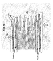
- Figure 14 detailed pictures of part of the three-dimensional structures are shown prior to depositing the conductive material: left the interdigitated electrodes and part of the isolation area and right a detail of the hills and the channels of the interdigitated electrodes and hills and channels of the isolation area.
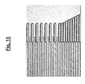
- Figure 15 a detailed picture of the interdigitated electrodes and part of the isolation area is shown after deposition of a thin gold layer.
- SEM-pictures show the three-dimensional structures: at the top left hills and channels at the edge of the electrode region near the isolation region; at the top right a detail of the hills in the electrode region is shown. At the bottom a zoom of the pictures at the top is shown near the hills, clearly illustrating the shadow zones near the hills and in the channels.
- an apparatus comprising an interdigitated electrode array.
- This apparatus comprises
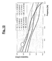
- Figure 18 shows the impedance part of the Bode plot showing the impedance characteristics of the three-dimensional structures in a silicon wafer, on which 100 nm DC-sputtered Ta 2 O 5 was deposited as an insulating film followed by the directional deposition of Au at an angle of 80° towards the surface normal.
- the impedance characteristics of the interdigitated electrodes resulting from this directional metal deposition (denoted SM) are compared to the response of silicon-based planar structures realised using deep UV lithography (denoted Si), which is the conventional way for processing interdigitated electrodes.
- the three-dimensional structures in a silicon wafer have channels with a width and spacing of 1 ⁇ m.
- the silicon-based planar structures realised using deep UV lithography have electrode width and spacings of 1 ⁇ m as well.
- the response of both types of interdigitated electrodes is shown for several concentration of KCl (i.e. 10 -1 , 10 2 and 10 -3 M) dispensed on top of the elecrodes.
- the interdigitated electrodes resulting from the directional metal deposition on the three-dimensional structures in a silicon wafer do not exhibit short circuits, indicating the effectiveness of the preferred embodiment for the isolation region.
- the impedimetric response of the interdigitated electrodes resulting from the directional metal deposition on the three-dimensional structures in a silicon wafer clearly changes as a function of the salt concentration, which is an indication of the formation of interdigitated electrodes to any person skilled in the art.
Landscapes
- Health & Medical Sciences (AREA)
- Life Sciences & Earth Sciences (AREA)
- Chemical & Material Sciences (AREA)
- Immunology (AREA)
- Engineering & Computer Science (AREA)
- Molecular Biology (AREA)
- Analytical Chemistry (AREA)
- Physics & Mathematics (AREA)
- General Health & Medical Sciences (AREA)
- Biochemistry (AREA)
- Organic Chemistry (AREA)
- Biomedical Technology (AREA)
- Urology & Nephrology (AREA)
- Wood Science & Technology (AREA)
- Zoology (AREA)
- Biotechnology (AREA)
- Microbiology (AREA)
- Hematology (AREA)
- Proteomics, Peptides & Aminoacids (AREA)
- Pathology (AREA)
- General Physics & Mathematics (AREA)
- Electrochemistry (AREA)
- Chemical Kinetics & Catalysis (AREA)
- Genetics & Genomics (AREA)
- Biophysics (AREA)
- Cell Biology (AREA)
- General Engineering & Computer Science (AREA)
- Bioinformatics & Cheminformatics (AREA)
- Food Science & Technology (AREA)
- Medicinal Chemistry (AREA)
- Investigating Or Analyzing Materials By The Use Of Electric Means (AREA)
- Apparatus Associated With Microorganisms And Enzymes (AREA)
Priority Applications (6)
| Application Number | Priority Date | Filing Date | Title |
|---|---|---|---|
| EP05109353A EP1772732A1 (fr) | 2005-10-07 | 2005-10-07 | Réseaux d'électrodes interdigités par réplication de polymères pour des applications de (bio)-détection |
| US12/089,528 US7955883B2 (en) | 2005-10-07 | 2006-09-06 | Polymer replicated interdigitated electrode array for (bio) sensing applications |
| PCT/EP2006/066069 WO2007042356A1 (fr) | 2005-10-07 | 2006-09-06 | Reseau d'electrodes interdigitees a replication polymere pour applications de (bio)detecteurs |
| AT06793271T ATE517337T1 (de) | 2005-10-07 | 2006-09-06 | Polymer-replizierte verflochtene elektroden- arrays für (bio)-sensoranwendungen |
| EP06793271A EP1931978B1 (fr) | 2005-10-07 | 2006-09-06 | Reseau d'electrodes interdigitees a replication polymere pour applications de (bio)detecteurs |
| US13/094,635 US20110201098A1 (en) | 2005-10-07 | 2011-04-26 | Polymer Replicated Interdigitated Electrode Array for Bio(Sensing) Applications |
Applications Claiming Priority (1)
| Application Number | Priority Date | Filing Date | Title |
|---|---|---|---|
| EP05109353A EP1772732A1 (fr) | 2005-10-07 | 2005-10-07 | Réseaux d'électrodes interdigités par réplication de polymères pour des applications de (bio)-détection |
Publications (2)
| Publication Number | Publication Date |
|---|---|
| EP1772732A1 true EP1772732A1 (fr) | 2007-04-11 |
| EP1772732A8 EP1772732A8 (fr) | 2007-06-13 |
Family
ID=35744864
Family Applications (2)
| Application Number | Title | Priority Date | Filing Date |
|---|---|---|---|
| EP05109353A Withdrawn EP1772732A1 (fr) | 2005-10-07 | 2005-10-07 | Réseaux d'électrodes interdigités par réplication de polymères pour des applications de (bio)-détection |
| EP06793271A Not-in-force EP1931978B1 (fr) | 2005-10-07 | 2006-09-06 | Reseau d'electrodes interdigitees a replication polymere pour applications de (bio)detecteurs |
Family Applications After (1)
| Application Number | Title | Priority Date | Filing Date |
|---|---|---|---|
| EP06793271A Not-in-force EP1931978B1 (fr) | 2005-10-07 | 2006-09-06 | Reseau d'electrodes interdigitees a replication polymere pour applications de (bio)detecteurs |
Country Status (4)
| Country | Link |
|---|---|
| US (2) | US7955883B2 (fr) |
| EP (2) | EP1772732A1 (fr) |
| AT (1) | ATE517337T1 (fr) |
| WO (1) | WO2007042356A1 (fr) |
Cited By (1)
| Publication number | Priority date | Publication date | Assignee | Title |
|---|---|---|---|---|
| CN111272819A (zh) * | 2020-02-21 | 2020-06-12 | 中山大学 | 心肌细胞多元活性检测的叉指排布导电纳米管传感装置 |
Families Citing this family (7)
| Publication number | Priority date | Publication date | Assignee | Title |
|---|---|---|---|---|
| ES2307430B1 (es) * | 2007-05-09 | 2009-10-20 | Consejo Superior De Investigaciones Cientificas | Biosensor y sus aplicaciones. |
| NZ630542A (en) | 2012-08-16 | 2017-06-30 | Ipierian Inc | Methods of treating a tauopathy |
| US20140072959A1 (en) | 2012-09-12 | 2014-03-13 | Force Diagnostics, Inc. | Rapid tests for insurance underwriting |
| US8980270B2 (en) | 2013-01-18 | 2015-03-17 | Ipierian, Inc. | Methods of treating a tauopathy |
| JP2017512751A (ja) | 2014-02-14 | 2017-05-25 | アイピエリアン,インコーポレイティド | タウペプチド、抗タウ抗体、およびそれらの使用方法 |
| WO2016133759A1 (fr) | 2015-02-20 | 2016-08-25 | Carbon3D, Inc. | Procédés et appareil pour l'impression à interface liquide continue (clip) avec zone morte assistée par voie électrochimique |
| CN107966478A (zh) * | 2016-10-19 | 2018-04-27 | 华邦电子股份有限公司 | 感测器阵列、其制造方法及感测方法 |
Citations (2)
| Publication number | Priority date | Publication date | Assignee | Title |
|---|---|---|---|---|
| EP0876601A1 (fr) | 1995-12-01 | 1998-11-11 | Innogenetics N.V. | Systeme de detection par mesure de l'impedance et procede pour le fabriquer |
| DE19950378A1 (de) * | 1999-10-19 | 2001-05-10 | Fraunhofer Ges Forschung | Verfahren zur Herstellung elektrischer Leiterstrukturen im Nanometerbereich sowie deren Verwendung als impedimetrischer Sensor |
Family Cites Families (2)
| Publication number | Priority date | Publication date | Assignee | Title |
|---|---|---|---|---|
| DE4201578A1 (de) * | 1992-01-22 | 1993-11-04 | Bosch Gmbh Robert | Kapazitiver sensor |
| JPH10335669A (ja) * | 1997-05-30 | 1998-12-18 | Mitsubishi Electric Corp | 薄膜トランジスタおよびその製法 |
-
2005
- 2005-10-07 EP EP05109353A patent/EP1772732A1/fr not_active Withdrawn
-
2006
- 2006-09-06 AT AT06793271T patent/ATE517337T1/de not_active IP Right Cessation
- 2006-09-06 EP EP06793271A patent/EP1931978B1/fr not_active Not-in-force
- 2006-09-06 WO PCT/EP2006/066069 patent/WO2007042356A1/fr not_active Ceased
- 2006-09-06 US US12/089,528 patent/US7955883B2/en not_active Expired - Fee Related
-
2011
- 2011-04-26 US US13/094,635 patent/US20110201098A1/en not_active Abandoned
Patent Citations (2)
| Publication number | Priority date | Publication date | Assignee | Title |
|---|---|---|---|---|
| EP0876601A1 (fr) | 1995-12-01 | 1998-11-11 | Innogenetics N.V. | Systeme de detection par mesure de l'impedance et procede pour le fabriquer |
| DE19950378A1 (de) * | 1999-10-19 | 2001-05-10 | Fraunhofer Ges Forschung | Verfahren zur Herstellung elektrischer Leiterstrukturen im Nanometerbereich sowie deren Verwendung als impedimetrischer Sensor |
Non-Patent Citations (5)
| Title |
|---|
| J. MICROMECH. MICROENG., vol. 10, 2000 |
| P. VAN GERWEN, J. MICROMECH. MICROENG., vol. 10, 2000 |
| SUGAWARA A ET AL: "SELF-ORGANIZED FE NANOWIRE ARRAYS PREPARED BY SHADOW DEPOSITION ON NACL(110) TEMPLATES", APPLIED PHYSICS LETTERS, AIP, AMERICAN INSTITUTE OF PHYSICS, MELVILLE, NY, US, vol. 70, no. 8, 24 February 1997 (1997-02-24), pages 1043 - 1045, XP000685188, ISSN: 0003-6951 * |
| VAN GERWEN ET AL.: "Cost Effective Realization of Nanoscaled Interdigitated Electrodes", JOURNAL OF MICROMECHANICS AND MICROENGINEERING, vol. 10, no. 3, September 2000 (2000-09-01), UK, pages N1 - N5, XP002367519 * |
| VAN GERWEN P ET AL: "Nanoscaled interdigitated electrode arrays for biochemical sensors", SENSORS AND ACTUATORS B, ELSEVIER SEQUOIA S.A., LAUSANNE, CH, vol. 49, no. 1-2, 25 June 1998 (1998-06-25), pages 73 - 80, XP004141441, ISSN: 0925-4005 * |
Cited By (1)
| Publication number | Priority date | Publication date | Assignee | Title |
|---|---|---|---|---|
| CN111272819A (zh) * | 2020-02-21 | 2020-06-12 | 中山大学 | 心肌细胞多元活性检测的叉指排布导电纳米管传感装置 |
Also Published As
| Publication number | Publication date |
|---|---|
| WO2007042356A1 (fr) | 2007-04-19 |
| EP1931978B1 (fr) | 2011-07-20 |
| US7955883B2 (en) | 2011-06-07 |
| US20090221446A1 (en) | 2009-09-03 |
| EP1931978A1 (fr) | 2008-06-18 |
| ATE517337T1 (de) | 2011-08-15 |
| US20110201098A1 (en) | 2011-08-18 |
| EP1772732A8 (fr) | 2007-06-13 |
Similar Documents
| Publication | Publication Date | Title |
|---|---|---|
| US20110201098A1 (en) | Polymer Replicated Interdigitated Electrode Array for Bio(Sensing) Applications | |
| CN109791120B (zh) | 用于分子传感器件的多电极结构及其制造方法 | |
| EP3540436B1 (fr) | Capteur moléculaire haute résolution | |
| KR100969667B1 (ko) | 생리활성물질을 전기적으로 검출하는 방법 및 이를 위한바이오칩 | |
| EP2088430A1 (fr) | Biocapteur doté d'électrodes en nanofils métalliques 3D formant un nanocanal, son procédé de fabrication et système de biodisques doté de celui-ci | |
| EP3391037B1 (fr) | Structures de fissures, jonctions tunnel utilisant des structures de fissures et leurs procédés de fabrication | |
| EP4182685B1 (fr) | Dispositif de détection de nanopores | |
| US20100052080A1 (en) | Biosensor chip and a method of manufacturing the same | |
| JP2000501503A (ja) | インピーダンス式検出システム及びその製造方法 | |
| WO2016202667A1 (fr) | Structure d'électrode et procédé de fabrication d'une structure d'électrode | |
| JP4196025B2 (ja) | バイオセンサーマトリックスおよびその製造方法 | |
| US20250060331A1 (en) | Methods of fabricating nanoscale structures usable in molecular sensors and other devices | |
| US20170350820A1 (en) | Biosensor for optical detection of nucleotide sequence | |
| KR101198460B1 (ko) | 플라스틱 바이오 센서 및 그 제조방법 | |
| KR20120038211A (ko) | 플라스틱 기반 바이오 센서 및 그 제조방법 |
Legal Events
| Date | Code | Title | Description |
|---|---|---|---|
| PUAI | Public reference made under article 153(3) epc to a published international application that has entered the european phase |
Free format text: ORIGINAL CODE: 0009012 |
|
| AK | Designated contracting states |
Kind code of ref document: A1 Designated state(s): AT BE BG CH CY CZ DE DK EE ES FI FR GB GR HU IE IS IT LI LT LU LV MC NL PL PT RO SE SI SK TR |
|
| AX | Request for extension of the european patent |
Extension state: AL BA HR MK YU |
|
| RAP1 | Party data changed (applicant data changed or rights of an application transferred) |
Owner name: INTERUNIVERSITAIR MICROELEKTRONICA CENTRUM (IMEC) Owner name: INNOGENETICS N.V. |
|
| RAP1 | Party data changed (applicant data changed or rights of an application transferred) |
Owner name: INNOGENETICS N.V. Owner name: INTERUNIVERSITAIR MICROELEKTRONICA CENTRUM VZW ( I |
|
| AKX | Designation fees paid | ||
| REG | Reference to a national code |
Ref country code: DE Ref legal event code: 8566 |
|
| STAA | Information on the status of an ep patent application or granted ep patent |
Free format text: STATUS: THE APPLICATION IS DEEMED TO BE WITHDRAWN |
|
| 18D | Application deemed to be withdrawn |
Effective date: 20071012 |