EP1772902A1 - Module semiconducteur de puissance avec couche isolante intermédiaire et méthode de fabrication - Google Patents
Module semiconducteur de puissance avec couche isolante intermédiaire et méthode de fabrication Download PDFInfo
- Publication number
- EP1772902A1 EP1772902A1 EP06020798A EP06020798A EP1772902A1 EP 1772902 A1 EP1772902 A1 EP 1772902A1 EP 06020798 A EP06020798 A EP 06020798A EP 06020798 A EP06020798 A EP 06020798A EP 1772902 A1 EP1772902 A1 EP 1772902A1
- Authority
- EP
- European Patent Office
- Prior art keywords
- power semiconductor
- semiconductor component
- insulating
- semiconductor device
- connection
- Prior art date
- Legal status (The legal status is an assumption and is not a legal conclusion. Google has not performed a legal analysis and makes no representation as to the accuracy of the status listed.)
- Granted
Links
Images
Classifications
-
- H—ELECTRICITY
- H10—SEMICONDUCTOR DEVICES; ELECTRIC SOLID-STATE DEVICES NOT OTHERWISE PROVIDED FOR
- H10W—GENERIC PACKAGES, INTERCONNECTIONS, CONNECTORS OR OTHER CONSTRUCTIONAL DETAILS OF DEVICES COVERED BY CLASS H10
- H10W90/00—Package configurations
-
- H—ELECTRICITY
- H10—SEMICONDUCTOR DEVICES; ELECTRIC SOLID-STATE DEVICES NOT OTHERWISE PROVIDED FOR
- H10W—GENERIC PACKAGES, INTERCONNECTIONS, CONNECTORS OR OTHER CONSTRUCTIONAL DETAILS OF DEVICES COVERED BY CLASS H10
- H10W40/00—Arrangements for thermal protection or thermal control
- H10W40/20—Arrangements for cooling
- H10W40/25—Arrangements for cooling characterised by their materials
- H10W40/255—Arrangements for cooling characterised by their materials having a laminate or multilayered structure, e.g. direct bond copper [DBC] ceramic substrates
-
- H—ELECTRICITY
- H10—SEMICONDUCTOR DEVICES; ELECTRIC SOLID-STATE DEVICES NOT OTHERWISE PROVIDED FOR
- H10W—GENERIC PACKAGES, INTERCONNECTIONS, CONNECTORS OR OTHER CONSTRUCTIONAL DETAILS OF DEVICES COVERED BY CLASS H10
- H10W70/00—Package substrates; Interposers; Redistribution layers [RDL]
- H10W70/60—Insulating or insulated package substrates; Interposers; Redistribution layers
- H10W70/611—Insulating or insulated package substrates; Interposers; Redistribution layers for connecting multiple chips together
-
- H—ELECTRICITY
- H10—SEMICONDUCTOR DEVICES; ELECTRIC SOLID-STATE DEVICES NOT OTHERWISE PROVIDED FOR
- H10W—GENERIC PACKAGES, INTERCONNECTIONS, CONNECTORS OR OTHER CONSTRUCTIONAL DETAILS OF DEVICES COVERED BY CLASS H10
- H10W90/00—Package configurations
- H10W90/401—Package configurations characterised by multiple insulating or insulated package substrates, interposers or RDLs
-
- H—ELECTRICITY
- H10—SEMICONDUCTOR DEVICES; ELECTRIC SOLID-STATE DEVICES NOT OTHERWISE PROVIDED FOR
- H10W—GENERIC PACKAGES, INTERCONNECTIONS, CONNECTORS OR OTHER CONSTRUCTIONAL DETAILS OF DEVICES COVERED BY CLASS H10
- H10W72/00—Interconnections or connectors in packages
- H10W72/071—Connecting or disconnecting
- H10W72/073—Connecting or disconnecting of die-attach connectors
- H10W72/07331—Connecting techniques
Definitions
- the invention describes a power semiconductor module comprising a housing with at least one electrically insulating substrate arranged therein, preferably for direct mounting on a heat sink.
- the substrate consists of an insulating body with a plurality of mutually insulated metallic interconnect tracks located thereon and power semiconductor components located thereon and connected in a circuitally correct manner to these interconnect tracks.
- the power semiconductor module has connection elements for external load and auxiliary connections and also connection elements for connections in the interior of the power semiconductor module. Furthermore, a method for producing a power semiconductor module mentioned above is described.
- Power semiconductor modules which are the starting point of this invention are known by way of example from US Pat DE 196 17 055 C1 , This document discloses a power semiconductor module of the above-mentioned type, wherein the power semiconductor components are arranged on the connecting tracks of the substrate by means of a solder connection.
- these substrates of such power semiconductor modules are designed as electrically insulating substrates consisting of an insulating body as carrier material and for electrical insulation to a base plate or to a heat sink.
- This Isolierstoff esp consists of the prior art from an industrial ceramics exemplified alumina or aluminum nitrite.
- On this insulating body on the inside of the power semiconductor module facing the first main surface are a plurality of mutually electrically insulated metallic interconnect tracks. In turn, the power semiconductor components are arranged on these.
- the insulating material body also has on its second main surface facing away from the interior of the power semiconductor module a metallic layer of the same material and the same thickness as that of the connecting tracks on the first main surface.
- this layer is not structured in itself, since it serves as an example of the solder joint to a base plate or the thermally conductive connection to a heat sink.
- the connecting tracks as well as the metallic layer of the second main surface preferably consist of copper applied by the DCB (direct copper bonding) method, the copper in this case having a typical thickness of less than 1 mm.
- connecting elements between the power semiconductor components and the connecting tracks are bonding connections and here especially wire bonds.
- the abovementioned document discloses as an alternative solution of the circuit-compatible connections of the power semiconductor components with each other and / or with interconnect tracks a flexible printed circuit board, which is flush with the power semiconductor devices and / or the interconnect tracks by means of solder connections or by means of pressure contact technology materially.
- the disclosed printed circuit board has a multilayer construction in order to provide both load connection connections as well as control and auxiliary connection connections.
- individual layers can be structured and / or connected to other layers or layer sections by means of plated-through holes.
- a variety of power semiconductor modules are known, which are in the range of power semiconductor components and above the connecting elements, which in this case are often designed as a bond, are cast with a potting compound with high dielectric constant.
- the above-mentioned document DE 196 17 055 C1 replaced such potting compounds by insulation liners, as they are known in principle from the production of printed circuit boards.
- These insulating intermediate layers comprise the power semiconductor components and have at their edge an edge covering which is intended to prevent voltage flashovers in this edge region.
- the insulation liners are formed such that they have the same thickness as the power semiconductor components which they comprise in order to thus form a planar surface for the arrangement of the flexible conductor track.
- a disadvantage of the embodiment of a power semiconductor module according to the cited document is that the insulating liners serve exclusively the internal insulation of the power semiconductor module and thus the production of such a trained power semiconductor module is more expensive compared to a potting compound with the same benefit, since the insulation liners adapted and in an additional Step must be treated by a precursor to a solid insulation layer.
- Another disadvantage is that the edges of the insulation liner must also be coated to safely prevent flashovers.
- Pressure sintering methods are known which disclose a permanent connection between a power semiconductor component and a connection element or a substrate.
- the disclosed methods are only suitable for the simultaneous sintering connection of a single power semiconductor component with a connection element or a substrate. This is due to the fact that in this case the pressure introduction can take place exclusively on the planar surface of the power semiconductor component.
- the known values of the pressure in the order of magnitude of 10 MPa to 60 MPa lead to a mechanical destruction of this edge region or of the power semiconductor component.
- the object of the invention is to present a power semiconductor module and an associated production method, wherein a means for internal isolation has a plurality of functions and is accessible for rational production.
- the inventive idea is based on a power semiconductor module, preferably for direct mounting on a heat sink or with a base plate.
- This power semiconductor module has at least the following components: a housing, connecting elements for load and auxiliary terminals, at least one substrate with connecting tracks and at least one power semiconductor component.
- connection elements for the load connections lead out of the housing and serve for the electrical connection of the power semiconductor components arranged inside the housing.
- the base plate or a heat sink electrically insulating formed substrate in turn consists of a Isolierstoff emotions, preferably an industrial ceramic, and thereon, on which the base plate or the heat sink facing away from the first main surface befindlich, a plurality of mutually electrically insulated metallic interconnect tracks.
- Power semiconductor components are arranged on these connecting tracks and are connected in a circuit-compatible manner by means of connecting elements.
- These connecting elements are here exemplified as a flexible printed circuit board according to the above-mentioned prior art or as a known busbar by means of stamped and bent metal-safe connecting rails.
- the power semiconductor module furthermore has at least one insulation molded body which surrounds at least one power semiconductor component and is deformed in a manner described below in such a way that it bears against and surrounds the edges of the associated power semiconductor component.
- the associated connecting element is configured in this case as a flexible printed circuit board, for example, and connects the power semiconductor component enclosed by the insulating molded body by way of example to a connecting element or a further power semiconductor component.
- the electrically conductive connection of the power semiconductor component to the associated conductor track of the substrate and / or to the connecting element, here the flexible printed circuit board, is designed as a pressure sintered connection.
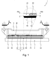
- FIG. 1 shows a power semiconductor module according to the invention in cross section.
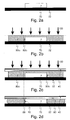
- Fig. 2 shows manufacturing steps of the method according to the invention.
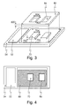
- Fig. 3 shows a three-dimensional representation of an arrangement of an insulating molded body and a substrate.
- FIG. 4 shows a plan view of the insulating molding and of the substrate according to FIG. 3.
- the power semiconductor module (1) has a housing (3) and a substrate (5) arranged therein, which consists of an insulating body (54) and of metallic laminations which are arranged on both main surfaces of the insulating body (54).
- the heat sink (2) facing metallic lamination (56) of the second main surface of the insulating body (54) is used for thermal coupling, is flat and not structured in itself.
- the lining of the first main surface of the insulating body (54) facing the power semiconductor module interior is structured in itself and thus forms the connecting tracks (52) of the substrate (5).
- the connecting elements (42, 44) of the power terminals are formed by metal moldings which are connected at their one end by way of example by soldering with the associated connecting track (52) and at its other end have a recess for screw connection.
- the power semiconductor components (70), shown here as power diodes, are arranged on the connection tracks (52).
- the circuit-compatible connection of the power diodes (70) with each other and with a connection element (40) is designed as a flexible printed circuit board (40).
- the electrically conductive connection between the power diodes (70) and the flexible printed circuit board (40) is designed as a pressure sintered connection, that between the power semiconductor component (70) and the connecting tracks (52) as a solder connection.
- the power semiconductor module has an insulation molding (80). This surrounds the power diodes (70) on all sides, wherein the contact surface (90) between the insulating molding (80) and the edge of the power semiconductor device (70) has a greater height (900) than half the thickness (700) of the power semiconductor device (70). This is crucial to prevent edge flashovers on the power semiconductor device (70). Furthermore, enough this insulating shaped body (80) to the connection element (42) of positive polarity and is electrically conductively connected to at least one surface of this connection element (42).
- the insulating molded body (80) in this case covers two printed conductors (52) and due to the described manufacturing method of the power semiconductor module (1) by means of pressure sintering technique, a portion of the insulating molded body (80) extends into the gap between the two conductor tracks (52).
- FIG. 2 shows manufacturing steps of the method according to the invention.
- a first embodiment variant of the method according to the invention is based on a substrate with a conductor track (52) arranged thereon.
- At least one power semiconductor component (70) with a suitably formed intermediate layer for pressure sintering connection is arranged on this conductor track (52) (FIG. 2 a).
- This power semiconductor component on all sides comprising an insulating molded body (80 a / b) is arranged (Fig. 2b).
- This preferably has a thickness between 2 of 100 and 10 of 100 greater than the thickness of the power semiconductor device (70).
- the distance between the edges of the power semiconductor device (70) and the comprehensive insulating molding (80) is preferably between 10/100 and 30/100 of the thickness of the power semiconductor device (70).
- This insulating shaped body (80) is preferably formed from a plastic which is deformable at least once under pressure and, if appropriate, additional temperature loading. A non-reversible deformation is particularly advantageous here.
- This deformation which is preferably associated with a preceding and / or simultaneous temperature application at a temperature between 50 ° C and 300 ° C, reduces the thickness of the insulating molded body (80) to the thickness of the power semiconductor device (70), wherein the insulating molded body (80 ) simultaneously expands laterally (86).
- the gap between the power semiconductor component (70) and insulating molded body (80) is closed, whereby this insulating molded body (80) thus surrounds the power semiconductor component (70) before the pressure is applied to the power semiconductor component (70).
- the contact surfaces (90) preferably have a height which is greater than half the thickness of the power semiconductor component (70). Due to the suitably chosen material of the insulating molding (80), this composite remains and serves in a power semiconductor module (1) of the inner insulation and prevented by its design during operation edge flashovers of the power semiconductor device (70).
- the insulation molding After completion of the pressure sintering process and in use in the power semiconductor module, the insulation molding has the same (FIG. 2 d) or a slightly greater thickness than the enclosed power semiconductor component.
- a flexible printed circuit board (40) or at least one connecting rail is arranged as a connecting element above the power semiconductor component (70) and on the insulating body (80) before the pressure sintering process (FIG. 2c).
- the areas that later form the contact surfaces between the power semiconductor device (70) and the connector (40) are prepared accordingly for a pressure sintering process.
- a suitable noble metal surface is formed on the power semiconductor component (70) and on the connecting element (40).
- a sintered metal is suitably arranged.
- a pressure sintered connection between this and the power semiconductor device (70) and at the same time between the power semiconductor device (70) and the conductor track (52) of the substrate (5) is formed.
- a third embodiment variant of the method according to the invention is based on a power semiconductor component (70) (FIG. 2 a) soldered onto the assigned conductor track (52) of a substrate (5), which is encompassed by an insulating die body (80) and wherein a flexible conductor track (40). is arranged on this.
- the sintering process thus creates a sintered connection between the power semiconductor component (70) and the connecting element (40).
- a plurality of power semiconductor components (70) can simultaneously be connected to printed conductors (52) and / or to connecting elements (40) in a single printing sintering process by arranging the insulating molded body (80).
- Fig. 3 shows a three-dimensional representation of the arrangement of the insulating molded body (80) and the substrate (5).
- the starting point for the production of the power semiconductor module (1) described with reference to FIG. 1 according to the manufacturing method described under FIG. 2 is a substrate according to the prior art.
- This has an insulating body (54), in this case an aluminum oxide ceramic, and copper conductor tracks (52) formed thereon.
- These copper conductor tracks (52) have a further layer of a noble metal, preferably gold, at least in those areas which serve as contact surfaces for a pressure sintered connection.
- the sintered metal is applied to these contact surfaces, preferably by means of a screen printing process.
- the power semiconductor components (70) are arranged.
- the power semiconductor components (70) comprising the insulating molded body (80) is then arranged. Its thickness is greater than that of the power semiconductor component (70) by 2 from 100 to 10 of 100.
- the length (802) of the recess (86) of the insulating molding (80) here is between 20 of 100 and 60 of 100 of the thickness of the power semiconductor device (70) greater than the length (702) of the power semiconductor device (70). The same applies to the width (804) of the recess (86) and the width (704) of the power semiconductor component (70).
- FIG. 4 shows a plan view of the insulating molded body (80) and the substrate (5) according to FIG. 3.
- the insulating molded body (80) shows a plan view of the insulating molded body (80) and the substrate (5) according to FIG. 3.
- the embracing of the power semiconductor component (70) by the insulating molded body (80) without these touching each other before the pressure sintering process, seen.
Landscapes
- Cooling Or The Like Of Semiconductors Or Solid State Devices (AREA)
- Die Bonding (AREA)
- Formation Of Insulating Films (AREA)
Applications Claiming Priority (1)
| Application Number | Priority Date | Filing Date | Title |
|---|---|---|---|
| DE102005047567A DE102005047567B3 (de) | 2005-10-05 | 2005-10-05 | Leistungshalbleitermodul mit Isolationszwischenlage und Verfahren zu seiner Herstellung |
Publications (2)
| Publication Number | Publication Date |
|---|---|
| EP1772902A1 true EP1772902A1 (fr) | 2007-04-11 |
| EP1772902B1 EP1772902B1 (fr) | 2008-09-17 |
Family
ID=37625994
Family Applications (1)
| Application Number | Title | Priority Date | Filing Date |
|---|---|---|---|
| EP06020798A Not-in-force EP1772902B1 (fr) | 2005-10-05 | 2006-10-04 | Module semiconducteur de puissance avec couche isolante intermédiaire et méthode de fabrication |
Country Status (6)
| Country | Link |
|---|---|
| EP (1) | EP1772902B1 (fr) |
| JP (1) | JP5291872B2 (fr) |
| AT (1) | ATE408898T1 (fr) |
| DE (2) | DE102005047567B3 (fr) |
| DK (1) | DK1772902T3 (fr) |
| ES (1) | ES2314804T3 (fr) |
Cited By (5)
| Publication number | Priority date | Publication date | Assignee | Title |
|---|---|---|---|---|
| DE102007006706A1 (de) * | 2007-02-10 | 2008-08-21 | Semikron Elektronik Gmbh & Co. Kg | Schaltungsanordnung mit Verbindungseinrichtung sowie Herstellungsverfahren hierzu |
| KR20100132469A (ko) * | 2009-06-09 | 2010-12-17 | 세미크론 엘렉트로니크 지엠비에치 앤드 코. 케이지 | 냉각장치를 포함하는 변환기 장치의 제조방법 및 변환기 장치 |
| EP2146372A3 (fr) * | 2008-07-16 | 2013-11-06 | Semikron Elektronik GmbH & Co. KG Patentabteilung | Dispositif de connexion électronique de puissance et son procédé de fabrication |
| DE102012222012A1 (de) | 2012-11-30 | 2014-06-18 | Semikron Elektronik Gmbh & Co. Kg | Leistungshalbleitereinrichtung und ein Verfahren zur Herstellung einer Leistungshalbleitereinrichtung |
| DE102013108185A1 (de) * | 2013-07-31 | 2015-02-05 | Semikron Elektronik Gmbh & Co. Kg | Verfahren zur Herstellung einer leistungselektronischen Schalteinrichtung und leistungselektronische Schalteinrichtung |
Families Citing this family (10)
| Publication number | Priority date | Publication date | Assignee | Title |
|---|---|---|---|---|
| DE102007022336A1 (de) * | 2007-05-12 | 2008-11-20 | Semikron Elektronik Gmbh & Co. Kg | Leistungshalbleitersubstrat mit Metallkontaktschicht sowie Herstellungsverfahren hierzu |
| DE102007057346B3 (de) * | 2007-11-28 | 2009-06-10 | Fachhochschule Kiel | Laminierte Leistungselektronikbaugruppe |
| DE102008017454B4 (de) | 2008-04-05 | 2010-02-04 | Semikron Elektronik Gmbh & Co. Kg | Leistungshalbleitermodul mit hermetisch dichter Schaltungsanordnung und Herstellungsverfahren hierzu |
| DE102008040488A1 (de) * | 2008-07-17 | 2010-01-21 | Robert Bosch Gmbh | Elektronische Baueinheit und Verfahren zu deren Herstellung |
| DE102009024385B4 (de) * | 2009-06-09 | 2011-03-17 | Semikron Elektronik Gmbh & Co. Kg | Verfahren zur Herstellung eines Leistungshalbleitermoduls und Leistungshalbleitermodul mit einer Verbindungseinrichtung |
| JP5842489B2 (ja) * | 2011-09-14 | 2016-01-13 | 三菱電機株式会社 | 半導体装置 |
| DE102011083911A1 (de) * | 2011-09-30 | 2013-04-04 | Robert Bosch Gmbh | Elektronische Baugruppe mit hochtemperaturstabilem Substratgrundwerkstoff |
| DE102014109779A1 (de) * | 2014-06-13 | 2015-12-17 | Osram Opto Semiconductors Gmbh | Verfahren zum Herstellen einer Anordnung mit einem Bauteil |
| DE102015109856A1 (de) * | 2015-06-19 | 2016-12-22 | Danfoss Silicon Power Gmbh | Verfahren zum Herstellen einer für die Anbindung eines elektrischen Leiters geeigneten metallischen Kontaktfläche zur Kontaktierung eines Leistungshalbleiters, Leistungshalbleiter, Bond Buffer und Verfahren zur Herstellung eines Leistungshalbleiters |
| DE102019126623B4 (de) | 2019-10-02 | 2024-03-14 | Semikron Elektronik Gmbh & Co. Kg Patentabteilung | Leistungselektronische Schalteinrichtung mit einer Vergussmasse |
Citations (3)
| Publication number | Priority date | Publication date | Assignee | Title |
|---|---|---|---|---|
| DE19617055C1 (de) * | 1996-04-29 | 1997-06-26 | Semikron Elektronik Gmbh | Halbleiterleistungsmodul hoher Packungsdichte in Mehrschichtbauweise |
| WO2005027222A2 (fr) * | 2003-09-12 | 2005-03-24 | Siemens Aktiengesellschaft | Composant electrique comportant une feuille d'isolation electrique disposee sur un substrat et procede de fabrication dudit dispositif |
| EP1538667A2 (fr) * | 2003-12-06 | 2005-06-08 | LuK Lamellen und Kupplungsbau Beteiligungs KG | Appareil électronique avec un corps dissipateur de chaleur metallique eléctriquement isolé |
Family Cites Families (5)
| Publication number | Priority date | Publication date | Assignee | Title |
|---|---|---|---|---|
| DE3414065A1 (de) * | 1984-04-13 | 1985-12-12 | Siemens AG, 1000 Berlin und 8000 München | Anordnung bestehend aus mindestens einem auf einem substrat befestigten elektronischen bauelement und verfahren zur herstellung einer derartigen anordnung |
| US4657322A (en) * | 1985-10-01 | 1987-04-14 | Tektronix, Inc. | Microwave interconnect |
| JPH08107266A (ja) * | 1994-10-04 | 1996-04-23 | Cmk Corp | プリント配線板 |
| DE10121970B4 (de) * | 2001-05-05 | 2004-05-27 | Semikron Elektronik Gmbh | Leistungshalbleitermodul in Druckkontaktierung |
| DE102004019567B3 (de) * | 2004-04-22 | 2006-01-12 | Semikron Elektronik Gmbh & Co. Kg | Verfahren zur Befestigung von elektronischen Bauelementen auf einem Substrat |
-
2005
- 2005-10-05 DE DE102005047567A patent/DE102005047567B3/de not_active Expired - Fee Related
-
2006
- 2006-10-04 ES ES06020798T patent/ES2314804T3/es active Active
- 2006-10-04 DE DE502006001588T patent/DE502006001588D1/de active Active
- 2006-10-04 EP EP06020798A patent/EP1772902B1/fr not_active Not-in-force
- 2006-10-04 AT AT06020798T patent/ATE408898T1/de active
- 2006-10-04 JP JP2006272882A patent/JP5291872B2/ja not_active Expired - Fee Related
- 2006-10-04 DK DK06020798T patent/DK1772902T3/da active
Patent Citations (3)
| Publication number | Priority date | Publication date | Assignee | Title |
|---|---|---|---|---|
| DE19617055C1 (de) * | 1996-04-29 | 1997-06-26 | Semikron Elektronik Gmbh | Halbleiterleistungsmodul hoher Packungsdichte in Mehrschichtbauweise |
| WO2005027222A2 (fr) * | 2003-09-12 | 2005-03-24 | Siemens Aktiengesellschaft | Composant electrique comportant une feuille d'isolation electrique disposee sur un substrat et procede de fabrication dudit dispositif |
| EP1538667A2 (fr) * | 2003-12-06 | 2005-06-08 | LuK Lamellen und Kupplungsbau Beteiligungs KG | Appareil électronique avec un corps dissipateur de chaleur metallique eléctriquement isolé |
Cited By (9)
| Publication number | Priority date | Publication date | Assignee | Title |
|---|---|---|---|---|
| DE102007006706A1 (de) * | 2007-02-10 | 2008-08-21 | Semikron Elektronik Gmbh & Co. Kg | Schaltungsanordnung mit Verbindungseinrichtung sowie Herstellungsverfahren hierzu |
| DE102007006706B4 (de) * | 2007-02-10 | 2011-05-26 | Semikron Elektronik Gmbh & Co. Kg | Schaltungsanordnung mit Verbindungseinrichtung sowie Herstellungsverfahren hierzu |
| EP2146372A3 (fr) * | 2008-07-16 | 2013-11-06 | Semikron Elektronik GmbH & Co. KG Patentabteilung | Dispositif de connexion électronique de puissance et son procédé de fabrication |
| KR20100132469A (ko) * | 2009-06-09 | 2010-12-17 | 세미크론 엘렉트로니크 지엠비에치 앤드 코. 케이지 | 냉각장치를 포함하는 변환기 장치의 제조방법 및 변환기 장치 |
| EP2271196A1 (fr) * | 2009-06-09 | 2011-01-05 | SEMIKRON Elektronik GmbH & Co. KG | Procédé de fabrication d'un dispositif de régulation du courant doté d'un dispositif de refroidissement et dispositif de régulation du courant |
| DE102012222012A1 (de) | 2012-11-30 | 2014-06-18 | Semikron Elektronik Gmbh & Co. Kg | Leistungshalbleitereinrichtung und ein Verfahren zur Herstellung einer Leistungshalbleitereinrichtung |
| DE102012222012B4 (de) * | 2012-11-30 | 2017-04-06 | Semikron Elektronik Gmbh & Co. Kg | Leistungshalbleitereinrichtung und ein Verfahren zur Herstellung einer Leistungshalbleitereinrichtung |
| DE102013108185A1 (de) * | 2013-07-31 | 2015-02-05 | Semikron Elektronik Gmbh & Co. Kg | Verfahren zur Herstellung einer leistungselektronischen Schalteinrichtung und leistungselektronische Schalteinrichtung |
| DE102013108185B4 (de) | 2013-07-31 | 2021-09-23 | Semikron Elektronik Gmbh & Co. Kg | Verfahren zur Herstellung einer leistungselektronischen Schalteinrichtung und leistungselektronische Schalteinrichtung |
Also Published As
| Publication number | Publication date |
|---|---|
| JP2007103948A (ja) | 2007-04-19 |
| DE102005047567B3 (de) | 2007-03-29 |
| JP5291872B2 (ja) | 2013-09-18 |
| ES2314804T3 (es) | 2009-03-16 |
| ATE408898T1 (de) | 2008-10-15 |
| DK1772902T3 (da) | 2009-01-19 |
| EP1772902B1 (fr) | 2008-09-17 |
| DE502006001588D1 (de) | 2008-10-30 |
Similar Documents
| Publication | Publication Date | Title |
|---|---|---|
| EP1956647B1 (fr) | Circuit doté d'un dispositif de liaison et son procédé de fabrication | |
| DE102008017454B4 (de) | Leistungshalbleitermodul mit hermetisch dichter Schaltungsanordnung und Herstellungsverfahren hierzu | |
| EP1713124B1 (fr) | Module semiconducteur de puissance avec des pistes de connexion et avec des éléments de connexion connectés aux pistes de connexion | |
| EP1772902B1 (fr) | Module semiconducteur de puissance avec couche isolante intermédiaire et méthode de fabrication | |
| DE102014116662B4 (de) | Elektrische anschlussbaugruppe, halbleitermodul und verfahren zurherstellung eines halbleitermoduls | |
| EP1830404A2 (fr) | Module semi-conducteur de puissance et son procédé de fabrication | |
| DE102009042600A1 (de) | Leistungshalbleitermodul und Herstellungsverfahren für dieses | |
| DE102009055691A1 (de) | Leistungshalbleitermodul | |
| DE102012211952B4 (de) | Leistungshalbleitermodul mit mindestens einem stressreduzierenden Anpasselement | |
| WO2013013964A1 (fr) | Dispositif support, dispositif électrique pourvu d'un dispositif support, et procédé de fabrication de ces dispositifs | |
| DE102005047566A1 (de) | Herstellungsverfahren und Anordnung mit einem Leistungshalbleiterbauelement und mit einem Gehäuse | |
| DE102004057421B4 (de) | Druckkontaktiertes Leistungshalbleitermodul für hohe Umgebungstemperaturen und Verfahren zu seiner Herstellung | |
| DE102014114808A1 (de) | Elektronikmodul und Verfahren zur Herstellung eines Elektronikmoduls | |
| DE102011078806B4 (de) | Herstellungsverfahren für ein leistungselektronisches System mit einer Kühleinrichtung | |
| DE102005050534B4 (de) | Leistungshalbleitermodul | |
| DE102005030247B4 (de) | Leistungshalbleitermodul mit Verbindungselementen hoher Stromtragfähigkeit | |
| DE202016101292U1 (de) | Leistungshalbleitereinrichtung | |
| EP2964004A2 (fr) | Agencement de composant electronique | |
| EP4189738A1 (fr) | Module de circuit électronique | |
| DE102016101726B4 (de) | Leistungshalbleitereinrichtung und Verfahren zur Herstellung einer Leistungshalbleitereinrichtung | |
| DE10121969C1 (de) | Schaltungsanordnung in Druckkontaktierung und Verfahren zu seiner Herstellung | |
| EP3012861B1 (fr) | Systeme de commutation et module de puissance | |
| DE102009050178B3 (de) | Leistungshalbleitermodul mit einem eine dreidimensionale Oberflächenkontur aufweisenden Substrat sowie Herstellungsverfahren hierzu | |
| DE102021116053A1 (de) | Elektrischer Leiter, elektronische Baugruppe mit elektrischem Leiter und Verfahren zum Herstellen einer elektronischen Baugruppe mit einem elektrischen Leiter | |
| DE102024110091A1 (de) | Leiterplattenanordnung |
Legal Events
| Date | Code | Title | Description |
|---|---|---|---|
| PUAI | Public reference made under article 153(3) epc to a published international application that has entered the european phase |
Free format text: ORIGINAL CODE: 0009012 |
|
| 17P | Request for examination filed |
Effective date: 20070205 |
|
| AK | Designated contracting states |
Kind code of ref document: A1 Designated state(s): AT BE BG CH CY CZ DE DK EE ES FI FR GB GR HU IE IS IT LI LT LU LV MC NL PL PT RO SE SI SK TR |
|
| AX | Request for extension of the european patent |
Extension state: AL BA HR MK YU |
|
| 17Q | First examination report despatched |
Effective date: 20070601 |
|
| AKX | Designation fees paid |
Designated state(s): AT BE BG CH CY CZ DE DK EE ES FI FR GB GR HU IE IS IT LI LT LU LV MC NL PL PT RO SE SI SK TR |
|
| GRAP | Despatch of communication of intention to grant a patent |
Free format text: ORIGINAL CODE: EPIDOSNIGR1 |
|
| GRAS | Grant fee paid |
Free format text: ORIGINAL CODE: EPIDOSNIGR3 |
|
| GRAA | (expected) grant |
Free format text: ORIGINAL CODE: 0009210 |
|
| AK | Designated contracting states |
Kind code of ref document: B1 Designated state(s): AT BE BG CH CY CZ DE DK EE ES FI FR GB GR HU IE IS IT LI LT LU LV MC NL PL PT RO SE SI SK TR |
|
| REG | Reference to a national code |
Ref country code: GB Ref legal event code: FG4D Free format text: NOT ENGLISH |
|
| REG | Reference to a national code |
Ref country code: CH Ref legal event code: EP |
|
| REG | Reference to a national code |
Ref country code: IE Ref legal event code: FG4D Free format text: LANGUAGE OF EP DOCUMENT: GERMAN |
|
| REF | Corresponds to: |
Ref document number: 502006001588 Country of ref document: DE Date of ref document: 20081030 Kind code of ref document: P |
|
| REG | Reference to a national code |
Ref country code: CH Ref legal event code: NV Representative=s name: BRAUNPAT BRAUN EDER AG |
|
| REG | Reference to a national code |
Ref country code: SE Ref legal event code: TRGR |
|
| REG | Reference to a national code |
Ref country code: DK Ref legal event code: T3 |
|
| PG25 | Lapsed in a contracting state [announced via postgrant information from national office to epo] |
Ref country code: LT Free format text: LAPSE BECAUSE OF FAILURE TO SUBMIT A TRANSLATION OF THE DESCRIPTION OR TO PAY THE FEE WITHIN THE PRESCRIBED TIME-LIMIT Effective date: 20080917 |
|
| PG25 | Lapsed in a contracting state [announced via postgrant information from national office to epo] |
Ref country code: LV Free format text: LAPSE BECAUSE OF FAILURE TO SUBMIT A TRANSLATION OF THE DESCRIPTION OR TO PAY THE FEE WITHIN THE PRESCRIBED TIME-LIMIT Effective date: 20080917 Ref country code: SI Free format text: LAPSE BECAUSE OF FAILURE TO SUBMIT A TRANSLATION OF THE DESCRIPTION OR TO PAY THE FEE WITHIN THE PRESCRIBED TIME-LIMIT Effective date: 20080917 |
|
| REG | Reference to a national code |
Ref country code: ES Ref legal event code: FG2A Ref document number: 2314804 Country of ref document: ES Kind code of ref document: T3 |
|
| REG | Reference to a national code |
Ref country code: IE Ref legal event code: FD4D |
|
| PG25 | Lapsed in a contracting state [announced via postgrant information from national office to epo] |
Ref country code: BG Free format text: LAPSE BECAUSE OF FAILURE TO SUBMIT A TRANSLATION OF THE DESCRIPTION OR TO PAY THE FEE WITHIN THE PRESCRIBED TIME-LIMIT Effective date: 20081217 |
|
| PG25 | Lapsed in a contracting state [announced via postgrant information from national office to epo] |
Ref country code: RO Free format text: LAPSE BECAUSE OF FAILURE TO SUBMIT A TRANSLATION OF THE DESCRIPTION OR TO PAY THE FEE WITHIN THE PRESCRIBED TIME-LIMIT Effective date: 20080917 Ref country code: PT Free format text: LAPSE BECAUSE OF FAILURE TO SUBMIT A TRANSLATION OF THE DESCRIPTION OR TO PAY THE FEE WITHIN THE PRESCRIBED TIME-LIMIT Effective date: 20090217 Ref country code: MC Free format text: LAPSE BECAUSE OF NON-PAYMENT OF DUE FEES Effective date: 20081031 Ref country code: IS Free format text: LAPSE BECAUSE OF FAILURE TO SUBMIT A TRANSLATION OF THE DESCRIPTION OR TO PAY THE FEE WITHIN THE PRESCRIBED TIME-LIMIT Effective date: 20090117 Ref country code: CZ Free format text: LAPSE BECAUSE OF FAILURE TO SUBMIT A TRANSLATION OF THE DESCRIPTION OR TO PAY THE FEE WITHIN THE PRESCRIBED TIME-LIMIT Effective date: 20080917 |
|
| PLBE | No opposition filed within time limit |
Free format text: ORIGINAL CODE: 0009261 |
|
| STAA | Information on the status of an ep patent application or granted ep patent |
Free format text: STATUS: NO OPPOSITION FILED WITHIN TIME LIMIT |
|
| PG25 | Lapsed in a contracting state [announced via postgrant information from national office to epo] |
Ref country code: IE Free format text: LAPSE BECAUSE OF FAILURE TO SUBMIT A TRANSLATION OF THE DESCRIPTION OR TO PAY THE FEE WITHIN THE PRESCRIBED TIME-LIMIT Effective date: 20080917 Ref country code: EE Free format text: LAPSE BECAUSE OF FAILURE TO SUBMIT A TRANSLATION OF THE DESCRIPTION OR TO PAY THE FEE WITHIN THE PRESCRIBED TIME-LIMIT Effective date: 20080917 |
|
| 26N | No opposition filed |
Effective date: 20090618 |
|
| PG25 | Lapsed in a contracting state [announced via postgrant information from national office to epo] |
Ref country code: PL Free format text: LAPSE BECAUSE OF FAILURE TO SUBMIT A TRANSLATION OF THE DESCRIPTION OR TO PAY THE FEE WITHIN THE PRESCRIBED TIME-LIMIT Effective date: 20080917 |
|
| PG25 | Lapsed in a contracting state [announced via postgrant information from national office to epo] |
Ref country code: CY Free format text: LAPSE BECAUSE OF FAILURE TO SUBMIT A TRANSLATION OF THE DESCRIPTION OR TO PAY THE FEE WITHIN THE PRESCRIBED TIME-LIMIT Effective date: 20080917 Ref country code: LU Free format text: LAPSE BECAUSE OF NON-PAYMENT OF DUE FEES Effective date: 20081004 |
|
| PG25 | Lapsed in a contracting state [announced via postgrant information from national office to epo] |
Ref country code: TR Free format text: LAPSE BECAUSE OF FAILURE TO SUBMIT A TRANSLATION OF THE DESCRIPTION OR TO PAY THE FEE WITHIN THE PRESCRIBED TIME-LIMIT Effective date: 20080917 |
|
| PG25 | Lapsed in a contracting state [announced via postgrant information from national office to epo] |
Ref country code: GR Free format text: LAPSE BECAUSE OF FAILURE TO SUBMIT A TRANSLATION OF THE DESCRIPTION OR TO PAY THE FEE WITHIN THE PRESCRIBED TIME-LIMIT Effective date: 20081218 |
|
| PGFP | Annual fee paid to national office [announced via postgrant information from national office to epo] |
Ref country code: FI Payment date: 20140710 Year of fee payment: 9 |
|
| PGFP | Annual fee paid to national office [announced via postgrant information from national office to epo] |
Ref country code: FR Payment date: 20140808 Year of fee payment: 9 |
|
| PGFP | Annual fee paid to national office [announced via postgrant information from national office to epo] |
Ref country code: DK Payment date: 20141003 Year of fee payment: 9 |
|
| PGFP | Annual fee paid to national office [announced via postgrant information from national office to epo] |
Ref country code: DE Payment date: 20141031 Year of fee payment: 9 Ref country code: GB Payment date: 20141022 Year of fee payment: 9 Ref country code: SE Payment date: 20141023 Year of fee payment: 9 Ref country code: CH Payment date: 20141030 Year of fee payment: 9 Ref country code: ES Payment date: 20141022 Year of fee payment: 9 Ref country code: SK Payment date: 20141001 Year of fee payment: 9 |
|
| PGFP | Annual fee paid to national office [announced via postgrant information from national office to epo] |
Ref country code: AT Payment date: 20140912 Year of fee payment: 9 Ref country code: HU Payment date: 20140718 Year of fee payment: 9 Ref country code: NL Payment date: 20141021 Year of fee payment: 9 |
|
| PGFP | Annual fee paid to national office [announced via postgrant information from national office to epo] |
Ref country code: IT Payment date: 20141023 Year of fee payment: 9 |
|
| PGFP | Annual fee paid to national office [announced via postgrant information from national office to epo] |
Ref country code: BE Payment date: 20141007 Year of fee payment: 9 |
|
| REG | Reference to a national code |
Ref country code: DE Ref legal event code: R119 Ref document number: 502006001588 Country of ref document: DE |
|
| REG | Reference to a national code |
Ref country code: DK Ref legal event code: EBP Effective date: 20151031 |
|
| REG | Reference to a national code |
Ref country code: SE Ref legal event code: EUG Ref country code: CH Ref legal event code: PL |
|
| REG | Reference to a national code |
Ref country code: AT Ref legal event code: MM01 Ref document number: 408898 Country of ref document: AT Kind code of ref document: T Effective date: 20151004 |
|
| GBPC | Gb: european patent ceased through non-payment of renewal fee |
Effective date: 20151004 |
|
| REG | Reference to a national code |
Ref country code: SK Ref legal event code: MM4A Ref document number: E 4711 Country of ref document: SK Effective date: 20151004 |
|
| REG | Reference to a national code |
Ref country code: NL Ref legal event code: MM Effective date: 20151101 |
|
| PG25 | Lapsed in a contracting state [announced via postgrant information from national office to epo] |
Ref country code: LI Free format text: LAPSE BECAUSE OF NON-PAYMENT OF DUE FEES Effective date: 20151031 Ref country code: IT Free format text: LAPSE BECAUSE OF NON-PAYMENT OF DUE FEES Effective date: 20151004 Ref country code: CH Free format text: LAPSE BECAUSE OF NON-PAYMENT OF DUE FEES Effective date: 20151031 Ref country code: DE Free format text: LAPSE BECAUSE OF NON-PAYMENT OF DUE FEES Effective date: 20160503 Ref country code: GB Free format text: LAPSE BECAUSE OF NON-PAYMENT OF DUE FEES Effective date: 20151004 |
|
| REG | Reference to a national code |
Ref country code: FR Ref legal event code: ST Effective date: 20160630 |
|
| PG25 | Lapsed in a contracting state [announced via postgrant information from national office to epo] |
Ref country code: NL Free format text: LAPSE BECAUSE OF NON-PAYMENT OF DUE FEES Effective date: 20151101 Ref country code: HU Free format text: LAPSE BECAUSE OF NON-PAYMENT OF DUE FEES Effective date: 20151005 Ref country code: FR Free format text: LAPSE BECAUSE OF NON-PAYMENT OF DUE FEES Effective date: 20151102 Ref country code: SE Free format text: LAPSE BECAUSE OF NON-PAYMENT OF DUE FEES Effective date: 20151005 Ref country code: SK Free format text: LAPSE BECAUSE OF NON-PAYMENT OF DUE FEES Effective date: 20151004 Ref country code: AT Free format text: LAPSE BECAUSE OF NON-PAYMENT OF DUE FEES Effective date: 20151004 |
|
| PG25 | Lapsed in a contracting state [announced via postgrant information from national office to epo] |
Ref country code: DK Free format text: LAPSE BECAUSE OF NON-PAYMENT OF DUE FEES Effective date: 20151031 |
|
| PG25 | Lapsed in a contracting state [announced via postgrant information from national office to epo] |
Ref country code: ES Free format text: LAPSE BECAUSE OF NON-PAYMENT OF DUE FEES Effective date: 20151005 Ref country code: FI Free format text: LAPSE BECAUSE OF NON-PAYMENT OF DUE FEES Effective date: 20151004 |
|
| PG25 | Lapsed in a contracting state [announced via postgrant information from national office to epo] |
Ref country code: BE Free format text: LAPSE BECAUSE OF NON-PAYMENT OF DUE FEES Effective date: 20151031 |
|
| REG | Reference to a national code |
Ref country code: ES Ref legal event code: FD2A Effective date: 20180709 |
|
| REG | Reference to a national code |
Ref country code: ES Ref legal event code: FD2A Effective date: 20180710 |