EP1775701A2 - Dispositif d'affichage à plasma et son procédé de commande - Google Patents
Dispositif d'affichage à plasma et son procédé de commande Download PDFInfo
- Publication number
- EP1775701A2 EP1775701A2 EP06255195A EP06255195A EP1775701A2 EP 1775701 A2 EP1775701 A2 EP 1775701A2 EP 06255195 A EP06255195 A EP 06255195A EP 06255195 A EP06255195 A EP 06255195A EP 1775701 A2 EP1775701 A2 EP 1775701A2
- Authority
- EP
- European Patent Office
- Prior art keywords
- electrodes
- voltage
- sustain
- subfield
- period
- Prior art date
- Legal status (The legal status is an assumption and is not a legal conclusion. Google has not performed a legal analysis and makes no representation as to the accuracy of the status listed.)
- Withdrawn
Links
Images





Classifications
-
- G—PHYSICS
- G09—EDUCATION; CRYPTOGRAPHY; DISPLAY; ADVERTISING; SEALS
- G09G—ARRANGEMENTS OR CIRCUITS FOR CONTROL OF INDICATING DEVICES USING STATIC MEANS TO PRESENT VARIABLE INFORMATION
- G09G3/00—Control arrangements or circuits, of interest only in connection with visual indicators other than cathode-ray tubes
- G09G3/20—Control arrangements or circuits, of interest only in connection with visual indicators other than cathode-ray tubes for presentation of an assembly of a number of characters, e.g. a page, by composing the assembly by combination of individual elements arranged in a matrix no fixed position being assigned to or needed to be assigned to the individual characters or partial characters
- G09G3/22—Control arrangements or circuits, of interest only in connection with visual indicators other than cathode-ray tubes for presentation of an assembly of a number of characters, e.g. a page, by composing the assembly by combination of individual elements arranged in a matrix no fixed position being assigned to or needed to be assigned to the individual characters or partial characters using controlled light sources
- G09G3/28—Control arrangements or circuits, of interest only in connection with visual indicators other than cathode-ray tubes for presentation of an assembly of a number of characters, e.g. a page, by composing the assembly by combination of individual elements arranged in a matrix no fixed position being assigned to or needed to be assigned to the individual characters or partial characters using controlled light sources using luminous gas-discharge panels, e.g. plasma panels
- G09G3/288—Control arrangements or circuits, of interest only in connection with visual indicators other than cathode-ray tubes for presentation of an assembly of a number of characters, e.g. a page, by composing the assembly by combination of individual elements arranged in a matrix no fixed position being assigned to or needed to be assigned to the individual characters or partial characters using controlled light sources using luminous gas-discharge panels, e.g. plasma panels using AC panels
- G09G3/291—Control arrangements or circuits, of interest only in connection with visual indicators other than cathode-ray tubes for presentation of an assembly of a number of characters, e.g. a page, by composing the assembly by combination of individual elements arranged in a matrix no fixed position being assigned to or needed to be assigned to the individual characters or partial characters using controlled light sources using luminous gas-discharge panels, e.g. plasma panels using AC panels controlling the gas discharge to control a cell condition, e.g. by means of specific pulse shapes
- G09G3/294—Control arrangements or circuits, of interest only in connection with visual indicators other than cathode-ray tubes for presentation of an assembly of a number of characters, e.g. a page, by composing the assembly by combination of individual elements arranged in a matrix no fixed position being assigned to or needed to be assigned to the individual characters or partial characters using controlled light sources using luminous gas-discharge panels, e.g. plasma panels using AC panels controlling the gas discharge to control a cell condition, e.g. by means of specific pulse shapes for lighting or sustain discharge
-
- G—PHYSICS
- G09—EDUCATION; CRYPTOGRAPHY; DISPLAY; ADVERTISING; SEALS
- G09G—ARRANGEMENTS OR CIRCUITS FOR CONTROL OF INDICATING DEVICES USING STATIC MEANS TO PRESENT VARIABLE INFORMATION
- G09G3/00—Control arrangements or circuits, of interest only in connection with visual indicators other than cathode-ray tubes
- G09G3/20—Control arrangements or circuits, of interest only in connection with visual indicators other than cathode-ray tubes for presentation of an assembly of a number of characters, e.g. a page, by composing the assembly by combination of individual elements arranged in a matrix no fixed position being assigned to or needed to be assigned to the individual characters or partial characters
- G09G3/2007—Display of intermediate tones
- G09G3/2018—Display of intermediate tones by time modulation using two or more time intervals
- G09G3/2022—Display of intermediate tones by time modulation using two or more time intervals using sub-frames
-
- G—PHYSICS
- G09—EDUCATION; CRYPTOGRAPHY; DISPLAY; ADVERTISING; SEALS
- G09G—ARRANGEMENTS OR CIRCUITS FOR CONTROL OF INDICATING DEVICES USING STATIC MEANS TO PRESENT VARIABLE INFORMATION
- G09G3/00—Control arrangements or circuits, of interest only in connection with visual indicators other than cathode-ray tubes
- G09G3/20—Control arrangements or circuits, of interest only in connection with visual indicators other than cathode-ray tubes for presentation of an assembly of a number of characters, e.g. a page, by composing the assembly by combination of individual elements arranged in a matrix no fixed position being assigned to or needed to be assigned to the individual characters or partial characters
- G09G3/22—Control arrangements or circuits, of interest only in connection with visual indicators other than cathode-ray tubes for presentation of an assembly of a number of characters, e.g. a page, by composing the assembly by combination of individual elements arranged in a matrix no fixed position being assigned to or needed to be assigned to the individual characters or partial characters using controlled light sources
- G09G3/28—Control arrangements or circuits, of interest only in connection with visual indicators other than cathode-ray tubes for presentation of an assembly of a number of characters, e.g. a page, by composing the assembly by combination of individual elements arranged in a matrix no fixed position being assigned to or needed to be assigned to the individual characters or partial characters using controlled light sources using luminous gas-discharge panels, e.g. plasma panels
- G09G3/288—Control arrangements or circuits, of interest only in connection with visual indicators other than cathode-ray tubes for presentation of an assembly of a number of characters, e.g. a page, by composing the assembly by combination of individual elements arranged in a matrix no fixed position being assigned to or needed to be assigned to the individual characters or partial characters using controlled light sources using luminous gas-discharge panels, e.g. plasma panels using AC panels
- G09G3/291—Control arrangements or circuits, of interest only in connection with visual indicators other than cathode-ray tubes for presentation of an assembly of a number of characters, e.g. a page, by composing the assembly by combination of individual elements arranged in a matrix no fixed position being assigned to or needed to be assigned to the individual characters or partial characters using controlled light sources using luminous gas-discharge panels, e.g. plasma panels using AC panels controlling the gas discharge to control a cell condition, e.g. by means of specific pulse shapes
- G09G3/292—Control arrangements or circuits, of interest only in connection with visual indicators other than cathode-ray tubes for presentation of an assembly of a number of characters, e.g. a page, by composing the assembly by combination of individual elements arranged in a matrix no fixed position being assigned to or needed to be assigned to the individual characters or partial characters using controlled light sources using luminous gas-discharge panels, e.g. plasma panels using AC panels controlling the gas discharge to control a cell condition, e.g. by means of specific pulse shapes for reset discharge, priming discharge or erase discharge occurring in a phase other than addressing
- G09G3/2927—Details of initialising
-
- G—PHYSICS
- G09—EDUCATION; CRYPTOGRAPHY; DISPLAY; ADVERTISING; SEALS
- G09G—ARRANGEMENTS OR CIRCUITS FOR CONTROL OF INDICATING DEVICES USING STATIC MEANS TO PRESENT VARIABLE INFORMATION
- G09G3/00—Control arrangements or circuits, of interest only in connection with visual indicators other than cathode-ray tubes
- G09G3/20—Control arrangements or circuits, of interest only in connection with visual indicators other than cathode-ray tubes for presentation of an assembly of a number of characters, e.g. a page, by composing the assembly by combination of individual elements arranged in a matrix no fixed position being assigned to or needed to be assigned to the individual characters or partial characters
- G09G3/22—Control arrangements or circuits, of interest only in connection with visual indicators other than cathode-ray tubes for presentation of an assembly of a number of characters, e.g. a page, by composing the assembly by combination of individual elements arranged in a matrix no fixed position being assigned to or needed to be assigned to the individual characters or partial characters using controlled light sources
- G09G3/28—Control arrangements or circuits, of interest only in connection with visual indicators other than cathode-ray tubes for presentation of an assembly of a number of characters, e.g. a page, by composing the assembly by combination of individual elements arranged in a matrix no fixed position being assigned to or needed to be assigned to the individual characters or partial characters using controlled light sources using luminous gas-discharge panels, e.g. plasma panels
- G09G3/288—Control arrangements or circuits, of interest only in connection with visual indicators other than cathode-ray tubes for presentation of an assembly of a number of characters, e.g. a page, by composing the assembly by combination of individual elements arranged in a matrix no fixed position being assigned to or needed to be assigned to the individual characters or partial characters using controlled light sources using luminous gas-discharge panels, e.g. plasma panels using AC panels
- G09G3/291—Control arrangements or circuits, of interest only in connection with visual indicators other than cathode-ray tubes for presentation of an assembly of a number of characters, e.g. a page, by composing the assembly by combination of individual elements arranged in a matrix no fixed position being assigned to or needed to be assigned to the individual characters or partial characters using controlled light sources using luminous gas-discharge panels, e.g. plasma panels using AC panels controlling the gas discharge to control a cell condition, e.g. by means of specific pulse shapes
- G09G3/293—Control arrangements or circuits, of interest only in connection with visual indicators other than cathode-ray tubes for presentation of an assembly of a number of characters, e.g. a page, by composing the assembly by combination of individual elements arranged in a matrix no fixed position being assigned to or needed to be assigned to the individual characters or partial characters using controlled light sources using luminous gas-discharge panels, e.g. plasma panels using AC panels controlling the gas discharge to control a cell condition, e.g. by means of specific pulse shapes for address discharge
- G09G3/2932—Addressed by writing selected cells that are in an OFF state
-
- G—PHYSICS
- G09—EDUCATION; CRYPTOGRAPHY; DISPLAY; ADVERTISING; SEALS
- G09G—ARRANGEMENTS OR CIRCUITS FOR CONTROL OF INDICATING DEVICES USING STATIC MEANS TO PRESENT VARIABLE INFORMATION
- G09G3/00—Control arrangements or circuits, of interest only in connection with visual indicators other than cathode-ray tubes
- G09G3/20—Control arrangements or circuits, of interest only in connection with visual indicators other than cathode-ray tubes for presentation of an assembly of a number of characters, e.g. a page, by composing the assembly by combination of individual elements arranged in a matrix no fixed position being assigned to or needed to be assigned to the individual characters or partial characters
- G09G3/22—Control arrangements or circuits, of interest only in connection with visual indicators other than cathode-ray tubes for presentation of an assembly of a number of characters, e.g. a page, by composing the assembly by combination of individual elements arranged in a matrix no fixed position being assigned to or needed to be assigned to the individual characters or partial characters using controlled light sources
- G09G3/28—Control arrangements or circuits, of interest only in connection with visual indicators other than cathode-ray tubes for presentation of an assembly of a number of characters, e.g. a page, by composing the assembly by combination of individual elements arranged in a matrix no fixed position being assigned to or needed to be assigned to the individual characters or partial characters using controlled light sources using luminous gas-discharge panels, e.g. plasma panels
- G09G3/288—Control arrangements or circuits, of interest only in connection with visual indicators other than cathode-ray tubes for presentation of an assembly of a number of characters, e.g. a page, by composing the assembly by combination of individual elements arranged in a matrix no fixed position being assigned to or needed to be assigned to the individual characters or partial characters using controlled light sources using luminous gas-discharge panels, e.g. plasma panels using AC panels
- G09G3/291—Control arrangements or circuits, of interest only in connection with visual indicators other than cathode-ray tubes for presentation of an assembly of a number of characters, e.g. a page, by composing the assembly by combination of individual elements arranged in a matrix no fixed position being assigned to or needed to be assigned to the individual characters or partial characters using controlled light sources using luminous gas-discharge panels, e.g. plasma panels using AC panels controlling the gas discharge to control a cell condition, e.g. by means of specific pulse shapes
- G09G3/293—Control arrangements or circuits, of interest only in connection with visual indicators other than cathode-ray tubes for presentation of an assembly of a number of characters, e.g. a page, by composing the assembly by combination of individual elements arranged in a matrix no fixed position being assigned to or needed to be assigned to the individual characters or partial characters using controlled light sources using luminous gas-discharge panels, e.g. plasma panels using AC panels controlling the gas discharge to control a cell condition, e.g. by means of specific pulse shapes for address discharge
- G09G3/2935—Addressed by erasing selected cells that are in an ON state
-
- G—PHYSICS
- G09—EDUCATION; CRYPTOGRAPHY; DISPLAY; ADVERTISING; SEALS
- G09G—ARRANGEMENTS OR CIRCUITS FOR CONTROL OF INDICATING DEVICES USING STATIC MEANS TO PRESENT VARIABLE INFORMATION
- G09G3/00—Control arrangements or circuits, of interest only in connection with visual indicators other than cathode-ray tubes
- G09G3/20—Control arrangements or circuits, of interest only in connection with visual indicators other than cathode-ray tubes for presentation of an assembly of a number of characters, e.g. a page, by composing the assembly by combination of individual elements arranged in a matrix no fixed position being assigned to or needed to be assigned to the individual characters or partial characters
- G09G3/22—Control arrangements or circuits, of interest only in connection with visual indicators other than cathode-ray tubes for presentation of an assembly of a number of characters, e.g. a page, by composing the assembly by combination of individual elements arranged in a matrix no fixed position being assigned to or needed to be assigned to the individual characters or partial characters using controlled light sources
- G09G3/28—Control arrangements or circuits, of interest only in connection with visual indicators other than cathode-ray tubes for presentation of an assembly of a number of characters, e.g. a page, by composing the assembly by combination of individual elements arranged in a matrix no fixed position being assigned to or needed to be assigned to the individual characters or partial characters using controlled light sources using luminous gas-discharge panels, e.g. plasma panels
- G09G3/288—Control arrangements or circuits, of interest only in connection with visual indicators other than cathode-ray tubes for presentation of an assembly of a number of characters, e.g. a page, by composing the assembly by combination of individual elements arranged in a matrix no fixed position being assigned to or needed to be assigned to the individual characters or partial characters using controlled light sources using luminous gas-discharge panels, e.g. plasma panels using AC panels
- G09G3/296—Driving circuits for producing the waveforms applied to the driving electrodes
-
- G—PHYSICS
- G09—EDUCATION; CRYPTOGRAPHY; DISPLAY; ADVERTISING; SEALS
- G09G—ARRANGEMENTS OR CIRCUITS FOR CONTROL OF INDICATING DEVICES USING STATIC MEANS TO PRESENT VARIABLE INFORMATION
- G09G3/00—Control arrangements or circuits, of interest only in connection with visual indicators other than cathode-ray tubes
- G09G3/20—Control arrangements or circuits, of interest only in connection with visual indicators other than cathode-ray tubes for presentation of an assembly of a number of characters, e.g. a page, by composing the assembly by combination of individual elements arranged in a matrix no fixed position being assigned to or needed to be assigned to the individual characters or partial characters
- G09G3/22—Control arrangements or circuits, of interest only in connection with visual indicators other than cathode-ray tubes for presentation of an assembly of a number of characters, e.g. a page, by composing the assembly by combination of individual elements arranged in a matrix no fixed position being assigned to or needed to be assigned to the individual characters or partial characters using controlled light sources
- G09G3/28—Control arrangements or circuits, of interest only in connection with visual indicators other than cathode-ray tubes for presentation of an assembly of a number of characters, e.g. a page, by composing the assembly by combination of individual elements arranged in a matrix no fixed position being assigned to or needed to be assigned to the individual characters or partial characters using controlled light sources using luminous gas-discharge panels, e.g. plasma panels
- G09G3/288—Control arrangements or circuits, of interest only in connection with visual indicators other than cathode-ray tubes for presentation of an assembly of a number of characters, e.g. a page, by composing the assembly by combination of individual elements arranged in a matrix no fixed position being assigned to or needed to be assigned to the individual characters or partial characters using controlled light sources using luminous gas-discharge panels, e.g. plasma panels using AC panels
- G09G3/298—Control arrangements or circuits, of interest only in connection with visual indicators other than cathode-ray tubes for presentation of an assembly of a number of characters, e.g. a page, by composing the assembly by combination of individual elements arranged in a matrix no fixed position being assigned to or needed to be assigned to the individual characters or partial characters using controlled light sources using luminous gas-discharge panels, e.g. plasma panels using AC panels using surface discharge panels
- G09G3/299—Control arrangements or circuits, of interest only in connection with visual indicators other than cathode-ray tubes for presentation of an assembly of a number of characters, e.g. a page, by composing the assembly by combination of individual elements arranged in a matrix no fixed position being assigned to or needed to be assigned to the individual characters or partial characters using controlled light sources using luminous gas-discharge panels, e.g. plasma panels using AC panels using surface discharge panels using alternate lighting of surface-type panels
-
- G—PHYSICS
- G09—EDUCATION; CRYPTOGRAPHY; DISPLAY; ADVERTISING; SEALS
- G09G—ARRANGEMENTS OR CIRCUITS FOR CONTROL OF INDICATING DEVICES USING STATIC MEANS TO PRESENT VARIABLE INFORMATION
- G09G2310/00—Command of the display device
- G09G2310/02—Addressing, scanning or driving the display screen or processing steps related thereto
- G09G2310/0202—Addressing of scan or signal lines
- G09G2310/0205—Simultaneous scanning of several lines in flat panels
- G09G2310/021—Double addressing, i.e. scanning two or more lines, e.g. lines 2 and 3; 4 and 5, at a time in a first field, followed by scanning two or more lines in another combination, e.g. lines 1 and 2; 3 and 4, in a second field
-
- G—PHYSICS
- G09—EDUCATION; CRYPTOGRAPHY; DISPLAY; ADVERTISING; SEALS
- G09G—ARRANGEMENTS OR CIRCUITS FOR CONTROL OF INDICATING DEVICES USING STATIC MEANS TO PRESENT VARIABLE INFORMATION
- G09G2310/00—Command of the display device
- G09G2310/02—Addressing, scanning or driving the display screen or processing steps related thereto
- G09G2310/0202—Addressing of scan or signal lines
- G09G2310/0218—Addressing of scan or signal lines with collection of electrodes in groups for n-dimensional addressing
-
- G—PHYSICS
- G09—EDUCATION; CRYPTOGRAPHY; DISPLAY; ADVERTISING; SEALS
- G09G—ARRANGEMENTS OR CIRCUITS FOR CONTROL OF INDICATING DEVICES USING STATIC MEANS TO PRESENT VARIABLE INFORMATION
- G09G2320/00—Control of display operating conditions
- G09G2320/02—Improving the quality of display appearance
- G09G2320/0238—Improving the black level
-
- G—PHYSICS
- G09—EDUCATION; CRYPTOGRAPHY; DISPLAY; ADVERTISING; SEALS
- G09G—ARRANGEMENTS OR CIRCUITS FOR CONTROL OF INDICATING DEVICES USING STATIC MEANS TO PRESENT VARIABLE INFORMATION
- G09G3/00—Control arrangements or circuits, of interest only in connection with visual indicators other than cathode-ray tubes
- G09G3/20—Control arrangements or circuits, of interest only in connection with visual indicators other than cathode-ray tubes for presentation of an assembly of a number of characters, e.g. a page, by composing the assembly by combination of individual elements arranged in a matrix no fixed position being assigned to or needed to be assigned to the individual characters or partial characters
- G09G3/2007—Display of intermediate tones
- G09G3/2018—Display of intermediate tones by time modulation using two or more time intervals
- G09G3/2022—Display of intermediate tones by time modulation using two or more time intervals using sub-frames
- G09G3/204—Display of intermediate tones by time modulation using two or more time intervals using sub-frames the sub-frames being organized in consecutive sub-frame groups
Definitions
- the present invention relates to a plasma display device and a driving method thereof.
- a plasma display device is a flat panel display that uses plasma generated by a gas discharge process to display characters or images. It includes a plurality of discharge cells arranged in a matrix pattern.
- One frame of the plasma display device is divided into a plurality of subfields each having a corresponding weight.
- a turn-on discharge cell is selected from amongst a plurality of the discharge cells by performing an addressing discharge for an address period of each subfield, and the turn-on discharge cell is sustain-discharged for a sustain period of each subfield so as to display an image.
- a scan pulse is applied to display regions in order to select a turn-on discharge cell among discharge cells formed at crossing areas of the display regions and address electrodes.
- a scan circuit is required to apply the scan pulse to the respective display regions for selecting a display region.
- the scan circuits are coupled to their corresponding scan electrodes.
- the present invention provides a plasma display device for reducing the number of scan circuits and stably generating a weak discharge during a main reset period, and a driving method thereof.
- the plasma display device includes a plurality of first electrodes, a plurality of second electrodes, and a plurality of third electrodes formed in a direction crossing a direction of the plurality of first electrodes and the plurality of second electrodes.
- a plurality of on-cells are selected according to a first addressing method in which one or more of the on-cells are converted into non-emitting or off state.
- a first voltage which is a sustain discharge voltage
- a voltage is applied to the first and third electrodes for a voltage difference between the first electrodes and the third electrodes to be a second voltage that is greater than a voltage difference between the first and second electrodes in the sustain period of the first subfield.
- an on-cell is selected according to a second addressing method in which one or more of the off-cells are converted into a light emitting state and then a sustain-discharge is generated in the converted cells.
- Preferred features are set out in claims 2 to 13.
- a method for driving a plasma display device including a plurality of first electrodes, a plurality of second electrodes, and a plurality of third electrodes formed in a direction crossing a direction of the first and second electrodes.
- an on-cell is selected according to a first addressing method in which the on-cell is converted into a non-emitting or off state and then a sustain-discharge is generated in the converted cell, and for a first period, a discharge is generated in the cell converted into the non-emitting or off state by the first address method.
- a reset-discharge is generated for initializing all the discharge cells.
- a plasma display device comprising a plasma display panel and a driver.
- the plasma display panel includes a plurality of first electrodes, a plurality of second electrodes, and a plurality of third electrodes formed in a direction crossing the plurality of first electrodes and the plurality of second electrodes.
- the driver applies a voltage in order for a voltage difference between the plurality of first electrodes and the plurality of third electrodes during a first period located between a first subfield and a second subfield to be greater than a voltage difference between the first and second electrodes in a sustain period of the first subfield.
- the driver alternately applies a first voltage to the plurality of first electrodes and the plurality of second voltages during the sustain period according to a first addressing method for converting a cell from a light-emitting or on state into a non-emitting or off state.
- the driver uses a second addressing method for converting a cell from the off state into an on state. Preferred features are set out in claims 18 to 21.
- Wall charges mentioned in the following description mean charges formed and accumulated on a wall (e.g., a dielectric layer) close to an electrode of a discharge cell.
- a wall voltage means a potential formed on the wall of the discharge cell by the wall charge.
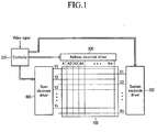
- a plasma display device according to an embodiment of the present invention and a driving method thereof will now be described with reference to FIG. 1, FIG. 2, and FIG. 3.
- the plasma display device includes a plasma display panel (PDP) 100, a controller 200, an address electrode driver 300, a scan electrode driver 400, and sustain electrode driver 500.
- PDP plasma display panel
- the PDP 100 includes a plurality of address electrodes A1 to Am extending in a column direction, and a plurality of sustain and scan electrodes X1 to Xn and Y1 to Yn extending in a row direction in pairs. This can be seen most easily in Figure 2.
- the controller 200 receives an external video signal and outputs an address electrode driving control signal, a sustain electrode driving control signal, and a scan electrode driving control signal. In addition, the controller 200 divides a frame into a plurality of subfields, each having a corresponding brightness weight, and drives the plasma display device during the subfields. In this particular embodiment, the controller 200 divides the plurality of sustain electrodes X1 to Xn into odd-numbered sustain electrodes Xodd and even-numbered sustain electrodes Xeven.
- the address electrode driver 300 After receiving the address electrode driving control signal from the controller 200, the address electrode driver 300 applies a data driving voltage to the address electrodes A1 to Am.
- the scan electrode driver 400 applies a scan driving voltage to the scan electrodes Y1 to Yn after receiving the scan electrode driving control signal from the controller 200.
- the sustain electrode driver 500 applies a sustain driving voltage to the sustain electrodes X1 to Xn after receiving the sustain electrode driving control signal from the controller 200.
- the address electrodes A1 to Am are formed on one substrate, and the sustain electrodes X1 to Xn and the scan electrodes Y1 to Yn are formed on another substrate, such that the two substrates may face each other.
- Display regions L1 to L(2n-1) for displaying an image are formed between two neighboring scan and sustain electrodes. For example, a display region L1 is formed between a first scan electrode Y1 and a first sustain electrode X1, and a display region L2 is formed between the first scan electrode Y1 and a second sustain electrode X2. That is, every two display regions L(2i-1) and L2i are formed by one scan electrode Yi and two sustain electrodes Xi and X(i+1) neighbouring the scan electrode Yi.
- the sustain electrodes X1 to Xn and the scan electrodes Y1 to Yn extend in a row direction; the sustain electrodes X1 to Xn each include a narrow bus electrode 31 a and a wide transparent electrode 31 b; and the scan electrodes Y1 to Yn each include a narrow bus electrode 32a and a wide transparent electrode 32b.
- the transparent electrodes 31 b and 32b are respectively coupled to the bus electrodes 31 a and 32a.
- the sustain and scan electrodes may be formed by a wide bus electrode without the transparent electrode, or formed by a transparent electrode without the bus electrode.
- the barrier rib 29 is formed on the bus electrodes 31 a and 32a such that the discharge cell 28 may be partitioned in a column direction.
- each sustain electrode since each sustain electrode, after the first sustain electrode, shares the two neighboring display regions with two neighboring scan electrodes, the number of sustain and scan electrodes may be reduced compared to a configuration in which each sustain electrode shares only one display region with a neighboring scan electrode on one side.
- the respective numbers of the sustain and scan electrodes are 512 of each type of electrode.
- the respective numbers of the sustain and scan electrodes are half of 512.
- the number of display regions of the PDP may be doubled while keeping the same number of sustain and scan electrodes of a conventional PDP where electrodes share one display region.
- the number of the sustain and scan electrodes may be reduced in half when the PDP is designed with the same resolution as a PDP including sustain and scan electrodes sharing one display region.
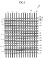
- FIG. 3 shows another electrode arrangement of a PDP according to a second embodiment of the present invention.
- a driving method applied to the configuration shown in FIG. 3 will now be described.
- the electrode arrangement of the PDP according to the second embodiment of the present invention is similar to that of the first embodiment, except that each sustain electrode shares only one display region with an adjacent scan electrode on one side. That is, in the PDP according to the second embodiment of the present invention, an additional barrier rib 29' is formed along the row direction between the scan electrode Y'i and the sustain electrode X'i+1. Therefore, while one display region is formed between the scan electrode Y'i and the sustain electrode X'i on one side, formation of a second display region on the other side of Y'i is prevented by the barrier rib 29'.
- transparent electrodes 31 b' and 32b' of the second embodiment need be formed only toward the one display region. This is in contrast to FIG. 2, where the transparent electrodes 31 b and 32b of the first embodiment appear on both sides of the narrow bus electrodes 31 a and 32a and extend toward both display regions on the two sides of a sustain or a scan electrode.
- the number of the display regions is reduced by half (i.e., n display regions) compared to the first embodiment.
- n display regions the number of sustain and scan electrodes that are required is doubled compared to the number of electrodes used in the first embodiment.
- a driving method to be described below is applied to the electrode arrangement according to the second embodiment of the present invention, a scan pulse is concurrently applied to two scan electrodes for an address period since one scan circuit is coupled to two scan electrodes.
- the driving method may however be applied to either the first or the second embodiment.
- a driving method for driving a plasma display device having a PDP according to either the first or second embodiment will now be described.
- the driving method will be described with reference to the first embodiment, shown in FIG. 2.
- the driving method for driving the PDP according to the second embodiment of the present invention shown in FIG. 3 is similar to that according to the first exemplary embodiment of the present invention except that the scan pulse applied for the address period of each subfield is concurrently applied to two scan electrodes.
- an odd cell a discharge cell on a display region formed between an odd-numbered sustain electrode Xodd and one of the scan electrodes Y1 to Yn
- an even cell a discharge cell on a display region formed between an even-numbered sustain electrode Xeven and one of the scan electrodes Y1 to Yn
- a discharge cell having enough wall charges to generate a sustain discharge for the sustain period will be referred to as an "on-cell,” and a discharge cell not having enough wall charges to generate the sustain discharge for the sustain period will be referred to as an "off-cell.”
- a reset period for reset discharging both sustain-discharged cells and cells not having been sustain-discharged in a previous subfield so as to initialize the cells will be referred to as a "main reset period MR.”
- a reset period for reset discharging only the cells that have been sustain-discharged in a previous subfield so as to initialize these cells will be referred to as a "selective reset period SR.”
- an address period for applying a write addressing method will be referred to as a "write address period WA,” and an address period for applying an erase addressing method will be referred to as an "erase address period EA.”
- the write addressing method is to discharge the cell in a non-emitting state so as to switch the non-e
- each odd or even frame is divided into a plurality of subfields SF1 to SF10.
- the subfields SF1 to SF10 each have a weight that may be predetermined.
- the weight of each subfield is included in parenthesis next to the subfield (e.g., SF1 (1) or SF5(8)). While FIG. 4 illustrates the subfields SF1 to SF10 as respectively having weights of 1, 2, 4, 8, 8, 8, 8, 8, and 8 the subfields SF1 to SF10 may have different weights in other embodiments.
- first to third subfields SF1 to SF3 of the odd-numbered frame subfield operations are performed for the odd cells but no operations are performed for the even cells.
- subfields operations are performed for the even cell to be driven, but no operations are performed for the odd cell. Accordingly, light is emitted in the first to third subfields SF1 to SF3 once every two frames. That is, in order for the first to third subfields SF1 to SF3, which are low grayscale subfields, to be realized by all of the cells including both the odd cells and the even cells, two frames (i.e., odd- and even-numbered frames) are required.
- the first subfield SF1 of the odd-numbered frame includes a main reset period MR, a write address period WA, and a sustain period S.
- the second and third subfields SF2 and SF3 each have a selective reset period SR, the write address period WA, and the sustain period S.
- operations of the reset, address, and sustain periods are performed for the odd cell.
- the reset periods of the second and third subfields SF2 and SF3 are shown as the selective reset period SR so as to shorten the reset period and increase a contrast ratio
- the main reset period MR may be substituted for the selective reset periods SR of the second and third subfields SF2 and SF3.
- the fifth to tenth subfields SF5 to SF10 each include first or second erase address periods EA1 and EA2 and first or second sustain periods S1 and S2 or the first sustain period S1 alone.
- an operation of the first erase address period EA1 and an operation of the first sustain period S1 are performed for the odd cell, and subsequently, an operation of the second erase address period EA2 and an operation of the second sustain period S2 are performed for the even cell.
- cells to be selected from the light emitted cells are set to the off state during the erase periods EA1 and EA2 of the fifth subfield SF5.
- cells to be set to the off state are selected from the cells sustain-discharged during the sustain period of the previous subfield (i.e., the on-cells).
- the sustain discharge may be generated in the odd cell and the even cell when a sustain pulse is applied to the odd-numbered sustain electrode Xodd and the even-numbered sustain electrode Xeven.
- a driving method of the even-numbered frame is similar to that of the odd-numbered frame described above, except that an order of the operations of the odd cell and the even cell is reversed. Therefore, detailed descriptions of the operation of the even-numbered frame is omitted. That is, during the even-numbered frame, the operations of the reset, write address, and sustain periods are performed only for the even cell in the first to third subfields SF1 to SF3, and in the fourth subfield SF4 the operations of the reset, write address, and sustain periods are performed for the odd cell after these operations are performed for the even cell. In the fifth to tenth subfields SF5 to SF10 of the even-numbered frame, the operations of the erase address period and the sustain period are performed for the even cells before these operations are performed for the odd cells.
- the weights of the fifth to tenth subfields SF5 to SF10 are the same as that of the fourth subfield SF4 because the cells selected during the erase address period and set to the off state may not be changed to the on state again in a subsequent subfield.
- the respective weights of the fifth to tenth subfields SF5 to SF10 may be set to a weight different and for example higher than 8. In this case, not all the 256 grayscales may be expressed. Accordingly, a dithering method may be used to express the 256 grayscale when the weights of the fifth to tenth subfields SF5 to SF10 are set to a value different from 8.
- Driving waveforms for using the driving method of FIG. 4 will now be described with reference to FIG. 5 to FIG. 8.
- the driving waveforms shown in FIG. 5 to FIG. 8 are applied to the odd-numbered frame, and driving waveforms applied to the even-numbered frame are not shown.
- Driving waveforms for the even-numbered frames may be realized when the driving waveforms applied to the odd-numbered sustain electrode Xodd are applied to the even-numbered sustain electrode Xeven and the driving waveforms applied to the even-numbered sustain electrode Xeven are applied to the odd-numbered sustain electrode Xodd. Therefore, only the driving waveforms applied to the odd-numbered frame will be described.
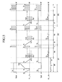
- FIG. 5 shows a diagram representing exemplary driving waveforms applied to the first to third subfields SF1 to SF3 according to the embodiments of the present invention.
- the first subfield includes the main reset period MR, the write address period WA, and the sustain period S
- the second and third subfields each include the selective reset period SR, the write address period WA, and the sustain period S.
- the main reset period MR of the first subfield SF1 includes an erase period I, a rising period II, and a falling period III.
- a voltage at the scan electrodes Y1 to Yn is gradually decreased from a voltage Vs to a reference voltage (0V in FIG. 5), while a voltage Ve is being applied to the odd-numbered sustain electrodes Xodd and the even-numbered sustain electrodes Xeven.
- the voltage Ve may be higher than the reference voltage 0V.
- FIG. 5 shows a gradually decreasing voltage as the erase waveform applied to the scan electrodes Y1 to Yn during the erase period I of the first subfield.
- a gradually increasing voltage may be applied to the sustain electrodes Xeven and Xodd while the voltage at the scan electrodes Y1 to Yn is at the reference voltage 0V, or a narrow pulse waveform for eliminating the wall charges may be substituted for the erase waveform.
- Xodd and Xeven indicate all the odd-numbered and all the even numbered sustain electrodes, respectively.
- the voltage at the scan electrodes Y1 to Yn is gradually increased from the Vs voltage to a Vset voltage while the Ve voltage is applied to the even-numbered sustain electrodes Xeven and the reference voltage 0V is applied to the odd-numbered sustain electrodes Xodd.
- the reference voltage 0V is applied to the address electrodes A1 to Am. Since the reference voltage 0V is applied to the odd-numbered sustain electrodes Xodd, a weak reset discharge occurs between an odd-numbered sustain electrode Xodd and a scan electrode forming a display region with the odd-numbered sustain electrode Xodd among the scan electrodes Y1 to Yn.
- the scan electrode forming the display region with the odd-numbered sustain electrode Xodd will be referred to as "Yxo.”
- the Yxo electrode indicates a scan electrode neighboring the odd-numbered sustain electrode Xodd, among all the scan electrodes Y1 to Yn, in an electrode arrangement according to the first embodiment of the present invention as shown in FIG. 2, and the Yxo electrode indicates the odd-numbered scan electrode Yodd in an electrode arrangement according to the second embodiment of the present invention as shown in FIG. 3.
- the scan electrode forming the display region with the even-numbered sustain electrode Xeven will be referred to as "Yxe.” That is, the Yxe electrode indicates a scan electrode neighboring the even-numbered sustain electrode Xeven, in the electrode arrangement according to the first embodiment of the present invention as shown in FIG. 2.
- the Yxe electrode also indicates a scan electrode neighboring an even-numbered sustain electrode Xeven in the electrode arrangement according to the second embodiment of the present invention as shown in FIG. 3.
- the reset discharge is not generated between the even-numbered sustain electrode Xeven and a scan electrode Yxe forming the display region with the even-numbered sustain electrode Xeven.
- a weak reset discharge is generated between the scan electrodes Y1 to Yn and the address electrodes A1 to Am. Accordingly, negative (-) wall charges are formed in the scan electrode area (transparent electrode) neighboring the odd-numbered sustain electrode Xodd in the electrode arrangement according to the first embodiment of the present invention as shown in FIG.
- the wall charges are formed such that a sum of an external voltage and a wall voltage may be maintained at a discharge firing voltage.
- the Vset voltage may be high enough to generate a discharge in the cells in every condition since all the odd cells, whether or not they were sustain-discharged in the previous subfield, are required to be initialized during the main reset period of the first subfield.
- the Vs voltage may be lower than a discharge firing voltage between the scan electrodes Y1 to Yn and the sustain electrodes X1 to Xn. While in FIG.
- the Vs voltage is set to be equal to the voltage of the sustain discharge pulse applied during the sustain period in order to reduce the number of power sources required, another voltage may be substituted for the Vs voltage.
- the Ve voltage may be selected such that the reset discharge may not be generated between the scan electrodes and the even-numbered sustain electrodes by a difference between the Vset voltage and the Ve voltage.
- the voltage at the scan electrodes Y1 to Yn is gradually decreased from the Vs voltage to a Vnf voltage.
- the reference voltage 0V is applied to the even-numbered scan electrodes Xeven
- the Ve voltage is applied to the odd-numbered scan electrodes Xodd
- the reference voltage 0V is applied to the address electrodes A1 to Am. While the voltage at the scan electrodes is decreased, a weak reset discharge occurs between the scan electrode Yxo and the odd-numbered sustain electrode Xodd and between the scan electrodes and the address electrodes.
- the Ve voltage and the Vnf voltage are set such that the wall voltage between the scan electrode Yxo and the odd-numbered sustain electrode Xodd may reach 0V, and therefore a misfiring in the cells that are not discharged in the address period may be prevented in the sustain period.
- the address electrodes A1 to Am are maintained at the reference voltage 0V, the wall voltage between the scan electrode Yxo and the address electrodes A1 to Am is determined by the level of the Vnf voltage.
- the reset discharge Since in the main reset period of the first subfield SF1, the reset discharge is generated only in the odd cell, the appropriate wall charges for the address operation are formed at the odd cell. However, appropriate wall charges for the address operation are not formed in the even cell since the reset discharge is not generated therein. In addition, the reset discharge changes the wall charge state of the odd cell and converts the cell into the off state.
- a scan pulse having a Vscl voltage is applied to the scan electrodes Y1 to Yn.
- the scan electrodes not receiving the Vscl voltage receive a Vsch voltage.
- the Vscl voltage is referred to as a scan voltage
- the Vsch voltage is referred to as a non-scan voltage.
- the scan pulse having the Vscl voltage is sequentially applied to the scan electrodes and the Vsch voltage is applied to the scan electrodes not receiving the Vscl voltage. For example, the scan pulse is applied to a Y(i+1) electrode after the scan pulse is applied to a Yi electrode.
- the scan pulse having the Vscl voltage is sequentially applied to pairs of neighboring scan electrodes (Y1 and Y2, Y3 and Y4, Y5 and Y6 ).
- the scan pulse is concurrently applied to Y(i+2) and Y(i+3) electrodes after the scan pulse is applied to Yi and Y(i+1) electrodes.
- the reference voltage 0V and the Ve voltage are respectively applied to the even-numbered sustain electrode Xeven and the odd-numbered sustain electrode Xodd.
- An address pulse having a Va voltage is applied to address electrodes passing through discharge cells to be selected from a plurality of discharge cells formed along the scan electrodes receiving the Vscl voltage. The other address electrodes are biased at the reference voltage 0V. Then, positive (+) wall charges are formed on the scan electrode, and negative (-) wall charges are formed on the address and sustain electrodes since a discharge is generated at a cell formed by the address electrode receiving the Va voltage, the scan electrode receiving the Vscl voltage, and the even-numbered sustain electrode Xeven receiving the Ve voltage.
- the cell receiving the Va voltage among the odd cells is changed from the off state to the on state since the address discharge is generated in this cell.
- the even cell was not initialized in the main reset period MR of the first subfield and the even-numbered sustain electrode Xeven is biased at the reference voltage for the write address period WA, the address discharge is not generated in the even cell. Since discharge cells are selected from the odd cells during the write address period WA of the first subfield SF1, the address pulse is applied to the address electrodes of the odd cells to select the discharge cells.
- the off-cell is changed to the on state due to the wall charges formed by discharging the cell. As a result, the cell is selected to emit light in the sustain period.
- a sustain pulse having the sustain discharge voltage Vs is alternately applied to the scan electrodes Y1 to Yn and both sets of the sustain electrodes Xodd and Xeven.
- the sustain discharge is generated by the sustain pulse in the cells that were set to the on state in the write address period WA of the first subfield.
- the number of the sustain pulses is appropriately selected according to the weight of the first subfield.
- Driving waveforms applied in the second subfield SF2 and the third subfield SF3 are similar to the driving waveform of the first subfield SF1 except for the driving waveforms applied for the reset period, and therefore detailed descriptions of them will be omitted.
- the voltage at the scan electrodes Y1 to Yn is gradually decreased from the Vs voltage to the Vnf voltage rather than being gradually increased, and therefore the cells sustain-discharged in the previous subfield are reset-discharged.
- negative (-) wall charges and positive (+) wall charges are respectively formed on the scan electrode and the sustain electrode of the sustain-discharged cell (i.e., the cell sustain-discharged in the first subfield among the odd cells) since the last sustain pulse is applied to the scan electrode.
- the reference voltage 0V and the Ve voltage are respectively applied to the even-numbered sustain electrode Xeven and the odd-numbered sustain electrode Xodd
- a voltage gradually decreased from the Vs voltage to the Vnf voltage is applied to the scan electrodes Y1 to Yn. Then, the reset discharge is generated in the cell sustain-discharged for the sustain period of the first subfield SF1.
- Reset discharge is not generated in the cells that were not sustain-discharged during the sustain period of the first subfield. However, it is not required to reset-discharge the cells that were not sustain-discharged in the first subfield among the odd cells since these cells are maintained at the wall charge state formed after the main reset period MR. Accordingly, the voltage that is gradually decreased from the Vs voltage to the Vnf voltage is appropriate to reset-discharge only the cells that were sustain-discharged in the first subfield SF1. In addition, for the selective reset period SR of the second subfield, since the Ve voltage is applied to the odd-numbered sustain electrode Xodd, the reset discharge is generated in the cell that is sustain-discharged in the first subfield SF1 among the odd cells.
- the voltage Ve prevents the other cells that do not have the appropriate wall charges from being reset. Therefore, after the selective reset period SR of the second subfield SF2, all the odd cells are initialized as off-cells.
- the odd cells that were sustain-discharged in the first subfield SF1 were reset-discharged and initialized during SR, and the odd cells that were not sustain-discharged in SF1 maintain the wall charge state formed after the main reset period MR of the first subfield SF1.
- Operation of the selective reset period SR of the third subfield SF3 is similar to that of the selective reset period SR of the second subfield, and therefore detailed description thereof will be omitted.
- the number of the sustain pulses for the sustain periods of the second subfield SF2 and the third subfield SF3 is appropriately selected according to the weight of the corresponding subfield.
- the reset, write address, and sustain discharge operations are performed by the driving waveforms shown in FIG. 5 in the odd cells during the first to third subfields SF1 to SF3.
- FIG. 6 shows the driving waveforms applied in the fourth subfield SF4 according to an embodiment of the present invention.
- the operations of the selective reset period SR, the first write address period WA1, and the first sustain period S1 are performed for the odd cell.
- the driving waveforms of the selective reset period SR, the first write address period WA1, and the first sustain period S1 in the fourth subfield are similar to those in the second subfield SF2 or the third subfield SF3, except that the number of sustain pulses applied for the first sustain period to set the weight is different, and therefore detailed description thereof will be omitted.
- the reset operation for initializing the odd cells as an off-cells is performed since the voltage at the scan electrodes Y1 to Yn is gradually decreased from the Vs voltage to the Vnf voltage while the Ve voltage is applied to the odd-numbered sustain electrodes Xodd.
- the write address operation for selecting the cells to be set as the on-cells among the odd cells is performed in the first write address period WA1.
- the sustain discharge operation is performed in the first sustain period S1 by alternately applying the sustain pulse to the scan electrodes Y1 to Yn and the sustain electrodes Xeven and Xodd.
- the voltage at the scan electrodes Y1 to Yn is gradually increased from the Vs voltage to the Vset voltage while the reference voltage 0V and the Ve voltage are respectively applied to the even-numbered sustain electrodes Xeven and the odd-numbered sustain electrodes Xodd.
- a voltage that is gradually decreased from the Vs voltage to the Vnf voltage is applied to the scan electrodes Y1 to Yn while the Ve voltage and the reference voltage 0V are respectively applied to the even-numbered sustain electrodes Xeven and the odd-numbered sustain electrodes Xodd.
- the driving waveforms applied to the even-numbered sustain electrodes Xeven and the odd-numbered sustain electrodes Xodd for the main reset period MR of the first subfield SF1 shown in FIG. 5 are switched between the two sets of electrodes in FIG. 6. Therefore, since the reset discharge is generated in the even cells, the even cells are initialized to the off state.
- the write address operation is performed in the even cells.
- the sustain discharge is generated in the cells selected during the second write address period WA2 since the sustain pulse is alternately applied to the scan electrodes Y1 to Yn and the sustain electrodes Xeven and Xodd.
- the cells sustain-discharged in the first sustain period S1 maintain their on state because no discharge was generated in these cells during the main reset period MR or the second write address period WA2. Accordingly, when the sustain pulse is applied in the second sustain period S2, sustain-discharge is also generated in the cells that were sustain-discharged during the first sustain period S1.
- the cells set to the on-state or the on state during both the first and second write address periods WA1 and WA2 are sustain-discharged during the second sustain period S2. Therefore, since the odd cells are sustain-discharged during both the first and second sustain periods, more sustain discharges are generated in the odd cells compared to the even cells.
- the last sustain pulse is applied to the scan electrodes Y1 to Yn. Accordingly, negative (-)and positive (+) wall charges are respectively formed on the scan electrode and the sustain electrode of the cell sustain-discharged in the first sustain period S1. These cells are on-cells due to the sustain discharge. Therefore, a wall voltage Vwxy is formed such that a potential of the sustain electrode is higher than that of the scan electrode.
- the wall charge state in the above cell is still maintained at the end of the main reset period MR since the reset discharge is not generated in the cell during the main reset period MR.
- FIG. 7 shows a diagram representing the driving waveforms applied during the fifth subfield SF5 among the driving waveforms of the plasma display device according to the exemplary embodiment of the present invention.
- the fifth subfield SF5 includes the first erase address period EA1 for the odd cells, the first sustain period S1, the second erase address period EA2 for the even cells, and the second sustain period S2.
- the cell is required to be in the on state. Since the cell that is sustain-discharged in the fourth subfield SF4 is in the on state, the first erase address period EA1 may be provided first in the fifth subfield SF5 as shown in FIG. 8.
- a ground voltage 0V and a Ve' voltage are respectively applied to the even-numbered sustain electrodes Xeven and the odd-numbered sustain electrodes Xodd.
- a scan voltage having a Vscl' voltage is sequentially applied to the scan electrodes Y1 to Yn and a Vsch' voltage is applied to the scan electrodes Y1 to Yn not receiving the Vscl' voltage in the electrode arrangement according to the first exemplary embodiment of the present invention.
- the scan pulse having the Vscl' voltage is sequentially applied to pairs of neighboring scan electrodes (Y1 and Y2, Y3 and Y4, Y5 and Y6,...) and the Vsch' voltage is applied to the scan electrodes not receiving the Vscl' voltage in the electrode arrangement according to the second exemplary embodiment of the present invention.
- the Ve' voltage is less than the Ve voltage applied for the write address period of the first to fourth subfields. Since the last sustain pulse is applied to the scan electrodes Y1 to Yn for the second sustain period S2 of the fourth subfield SF4, negative (-) and positive (+) wall charges are respectively formed on the scan and sustain electrodes of the cells sustain-discharged in the sustain period of the fourth subfield.
- the sustain discharge is generated between the scan electrode receiving the scan voltage Vscl' and the address electrode receiving the address voltage Va' since a difference of (Va'+
- the erase address operation may be performed by the scan voltage Vscl' and the address voltage Va' at the odd cells formed by the odd-numbered sustain electrodes Xodd receiving the Ve' voltage. But it may not be performed by the scan voltage Vscl' and the address voltage Va' at the even cells formed by the even-numbered sustain electrodes Xeven not receiving the Ve' voltage.
- the erase address operation may be determined depending on whether the Ve' voltage is applied. Therefore, in the first erase address period EA1, the erase address operation is performed at the cell selected from the odd cells since the cell state is converted from the light emitting state to the off state.
- the erase address operation may be performed by the Ve' voltage that is lower than the Ve voltage. Accordingly, a level of the Ve' voltage applied for the first erase address period EA1 is less than a level of the Ve voltage, as described above. However, the Ve voltage applied for the write address period of the first to fourth subfields SF1 to SF4 is set to a higher voltage since comparatively smaller amounts of wall charges are formed after the reset period.
- the scan voltage Vscl' and the non-scan voltage Vsch' for the first erase address period EA1 may be set respectively higher than the scan voltage Vscl and the non-scan voltage Vsch for the write address period of the first to fourth subfields SF1 to SF4. This is due to the fact that the erase operation of the first erase address period EA1 is to set the sustain-discharged cells to the off state.
- a width of the scan pulse applied for the first erase address period EA1 may be reduced to less than that applied for the write address period of the first to fourth subfields SF1 to SF4. Since the erase address operation is to change the on state to the off state, the scan pulse width for the erase address period may be reduced to less than that for the write address period not to provide time for forming wall charges by the discharge.
- the cell remaining in the on state is sustain-discharged by alternately applying the sustain pulse to the scan electrodes Y1 to Yn and the sustain electrodes Xodd and Xeven.
- the number of the sustain pulses is appropriately selected according to the weight of the fifth subfield SF5.
- the sustain pulses applied during the first sustain period S1 supplement the wall charges of the even cells that were lost in the first erase address period EA1.
- a weak discharge is generated between the scan and address electrodes of the even cells when the reference voltage 0V is applied to the even-numbered sustain electrode Xeven.
- the wall charges formed on the address electrode of the cells in the on state are eliminated.
- the erase address operation would not be appropriately performed at the cells in the on state among the even cells for the second erase address period EA2 since.
- the eliminated wall charges are supplemented by the operation of the first sustain period S1.
- the sustain discharge is generated at the light-emitting even cells when the sustain pulse is applied in the first sustain period S1 although some wall charges are eliminated in the first erase address period EA1.
- the eliminated wall charges are supplemented by the sustain discharge.
- the Ve' voltage and the reference voltage 0V are respectively applied to the even-numbered sustain electrodes Xeven and the odd-numbered sustain electrodes Xodd for the second erase address period EA2.
- the scan pulse having the Vscl' voltage is sequentially applied to the scan electrodes Y1 to Yn and the Vsch' voltage is applied to the scan electrodes not receiving the Vscl' voltage in the electrode arrangement according to the first embodiment of the present invention.
- the scan pulse having the Vscl' voltage is sequentially applied to pairs of neighboring scan electrodes (Y1 and Y2, Y3 and Y4, Y5 and Y6,...) and the Vsch' voltage is applied to the scan electrodes not receiving the Vscl' voltage in the electrode arrangement according to the second embodiment of the present invention. Since the Ve' voltage is applied to the even-numbered sustain electrodes Xeven, the cells to be selected as the off-cells are selected from the even cells in the second erase address period EA2 differing from the first erase address period EA1.
- the sustain pulse is alternately applied to the scan electrodes Y1 to Yn and the sustain electrodes Xodd and Xeven in the second sustain period S2. Then, the cells remaining in the light emitting state are sustain-discharged.
- the number of the sustain pulses applied during the second sustain period S2 is set to be equal to the number of the sustain pulses applied during the first sustain period S1.
- some wall charges of the odd cells remaining in the light emitting state are eliminated in the second erase address period EA2, but the eliminated wall charges are supplemented by the sustain discharge in the second sustain period S2 the same way they were supplemented during the first sustain period S1. Accordingly, the erase address operation is appropriately performed in the odd cells for the first erase address period EA1 of the sixth subfield SF6 following the fifth subfield SF5.
- the driving waveforms applied to the sixth to ninth subfields SF6 to SF9 are similar to those of the fifth subfield SF5 shown in FIG. 7, and therefore detailed descriptions thereof will be omitted.
- a difference between the wall charge state of the cells after the write address operation and the wall charge state of the cells having the wall charges eliminated due to the erase address operation after the fifth subfield SF5 may cause a problem in the main reset operation.
- the main reset is designed for the write address operation, and therefore it may not be properly performed in the cells having wall charges eliminated by the erase address operation.
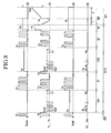
- a driving waveform of FIG. 8 is applied in the tenth subfield SF10 of the odd-numbered frame in order to stably perform the main reset operation during the next frame (even-numbered frame).
- FIG. 8 shows driving waveforms applied to the tenth subfield SF10
- FIG. 9A to FIG. 9C show the wall charge distribution applied to the plasma display device.
- Y represents an scan electrode selected from the plurality of scan electrodes Y1 to Yn
- A represents an address electrode selected from the plurality of address electrodes A1 to Am
- X represents a sustain electrode selected from the plurality of sustain electrodes Xodd and Xeven.
- the tenth subfield SF10 includes the first erase address period EA1 for the even cells, the first sustain period S1, the second erase address period EA2 for the odd cells, the second sustain period S2, and a correction period M for controlling the wall charge state.
- the erase address periods EA1 and EA2 and the first and second sustain periods S1 and S2 are similar to those shown in FIG. 7, and therefore detailed descriptions thereof will be omitted.
- the sustain discharge pulse is applied to the scan electrodes Y in the fifth to tenth subfields SF5 to SF10 and thus the wall charge state of the sustain-discharged cell becomes the wall charge state shown in FIG. 9A. That is, a relatively large amount of negative (-) wall charges is formed on the scan electrodes Y, and positive (+) wall charges are formed on the sustain electrodes Xodd and Xeven and the address electrodes A.
- a correction period M is added after the second sustain period S2 is performed in the tenth subfield SF10.
- a voltage Vc that is higher than the Vs voltage is applied to the scan electrodes Y during the correction period M. That is, a voltage difference between the address electrodes A and the scan electrodes Y becomes the voltage Vc which is greater than the voltage Vs when the voltage Vc is applied to the scan electrodes Y while the ground voltage is applied to the address electrodes A.
- the voltage Ve is applied to the sustain electrodes Xodd and Xeven. Therefore, positive (+) wall charges are formed on the address electrodes A and negative (-) wall charges are formed on the scan electrodes Y.
- the cells Prior to the correction period M, when the sustain-discharging is generated in the cells in the tenth subfield SF10, the cells maintain the same wall charge state shown in FIG. 9A even after the voltage Vc is applied. That is, the last sustain pulse is applied to the scan electrodes Y and thus negative (-) wall charges are formed thereon, and accordingly the wall charge state is not changed even though the voltage Vc is applied to the scan electrodes Y.
- the erase-addressed cell in the wall charge state of FIG. 9A is initialized by a weak reset discharge generated between the even cell and its neighboring scan electrode during the main reset period MR, and changed to the wall charge state of FIG. 9C.
- the voltage Vc can be set to be a sum of the Vs voltage, the Vsch voltage, and the Vscl voltage in order to reduce the number of power sources.
- the correction period M is included in the tenth subfield SF10 as shown in FIG. 8. However, the correction period M can be included in the reset period of the even-numbered frame instead.
- embodiments of the invention enable the number of electrodes can be reduced by sharing of the scan electrode by two neighboring display regions to thereby reduce the number of scan circuits.
- wall charge initialization can be appropriately performed in the next main reset period by adding the correction period.
Landscapes
- Engineering & Computer Science (AREA)
- Physics & Mathematics (AREA)
- Computer Hardware Design (AREA)
- General Physics & Mathematics (AREA)
- Theoretical Computer Science (AREA)
- Power Engineering (AREA)
- Plasma & Fusion (AREA)
- Control Of Indicators Other Than Cathode Ray Tubes (AREA)
- Control Of Gas Discharge Display Tubes (AREA)
Applications Claiming Priority (1)
| Application Number | Priority Date | Filing Date | Title |
|---|---|---|---|
| KR1020050095996A KR100728163B1 (ko) | 2005-10-12 | 2005-10-12 | 플라즈마 표시 장치 및 그 구동 방법 |
Publications (2)
| Publication Number | Publication Date |
|---|---|
| EP1775701A2 true EP1775701A2 (fr) | 2007-04-18 |
| EP1775701A3 EP1775701A3 (fr) | 2007-08-22 |
Family
ID=37517226
Family Applications (1)
| Application Number | Title | Priority Date | Filing Date |
|---|---|---|---|
| EP06255195A Withdrawn EP1775701A3 (fr) | 2005-10-12 | 2006-10-09 | Dispositif d'affichage à plasma et son procédé de commande |
Country Status (3)
| Country | Link |
|---|---|
| US (1) | US20070080899A1 (fr) |
| EP (1) | EP1775701A3 (fr) |
| KR (1) | KR100728163B1 (fr) |
Cited By (1)
| Publication number | Priority date | Publication date | Assignee | Title |
|---|---|---|---|---|
| EP1923853A3 (fr) * | 2006-11-20 | 2010-04-07 | Samsung SDI Co., Ltd. | Affichage à plasma et son procédé de commande |
Families Citing this family (1)
| Publication number | Priority date | Publication date | Assignee | Title |
|---|---|---|---|---|
| KR20090037675A (ko) | 2007-10-12 | 2009-04-16 | 삼성전자주식회사 | 영상신호처리장치 및 그의 영상신호처리방법 |
Family Cites Families (20)
| Publication number | Priority date | Publication date | Assignee | Title |
|---|---|---|---|---|
| US5745086A (en) * | 1995-11-29 | 1998-04-28 | Plasmaco Inc. | Plasma panel exhibiting enhanced contrast |
| JP3423865B2 (ja) * | 1997-09-18 | 2003-07-07 | 富士通株式会社 | Ac型pdpの駆動方法及びプラズマ表示装置 |
| US6356249B1 (en) * | 1999-07-19 | 2002-03-12 | Lg Electronics Inc. | Method of driving plasma display panel |
| JP4331359B2 (ja) * | 1999-11-18 | 2009-09-16 | 三菱電機株式会社 | 交流型プラズマディスプレイパネルの駆動方法 |
| KR100617446B1 (ko) * | 1999-11-30 | 2006-09-01 | 오리온피디피주식회사 | 플라즈마 디스플레이 패널의 구동방법 |
| US6653795B2 (en) * | 2000-03-14 | 2003-11-25 | Lg Electronics Inc. | Method and apparatus for driving plasma display panel using selective writing and selective erasure |
| US7075239B2 (en) * | 2000-03-14 | 2006-07-11 | Lg Electronics Inc. | Method and apparatus for driving plasma display panel using selective write and selective erase |
| JP2002023689A (ja) * | 2000-06-30 | 2002-01-23 | Pioneer Electronic Corp | プラズマディスプレイ装置 |
| US6956546B1 (en) * | 2000-10-10 | 2005-10-18 | Mitsubishi Denki Kabushiki Kaisha | Method of driving AC plasma display panel, plasma display device and AC plasma display panel |
| JP2002140033A (ja) * | 2000-11-02 | 2002-05-17 | Fujitsu Hitachi Plasma Display Ltd | プラズマディスプレイの駆動方法 |
| US7091935B2 (en) * | 2001-03-26 | 2006-08-15 | Lg Electronics Inc. | Method of driving plasma display panel using selective inversion address method |
| KR100438907B1 (ko) * | 2001-07-09 | 2004-07-03 | 엘지전자 주식회사 | 플라즈마 디스플레이 패널의 구동방법 |
| KR100480152B1 (ko) * | 2002-05-17 | 2005-04-06 | 엘지전자 주식회사 | 플라즈마 디스플레이 패널의 구동방법 |
| KR20040056047A (ko) * | 2002-12-23 | 2004-06-30 | 엘지전자 주식회사 | 선택적 쓰기 및 소거를 이용한 플라즈마 디스플레이패널의 구동방법 및 장치 |
| KR100563464B1 (ko) * | 2003-11-03 | 2006-03-23 | 엘지전자 주식회사 | 플라즈마 디스플레이 패널의 구동방법 |
| KR100563463B1 (ko) * | 2003-11-03 | 2006-03-23 | 엘지전자 주식회사 | 플라즈마 디스플레이 패널의 구동방법 |
| KR100524310B1 (ko) * | 2003-11-08 | 2005-10-28 | 엘지전자 주식회사 | 플라즈마 디스플레이 패널의 구동방법 |
| KR20050077823A (ko) * | 2004-01-28 | 2005-08-04 | 엘지전자 주식회사 | 휘도를 보상할 수 있는 플라즈마 표시 패널의 구동 방법 |
| KR100521468B1 (ko) * | 2004-03-19 | 2005-10-12 | 삼성에스디아이 주식회사 | 플라즈마 디스플레이 패널과 그 구동방법 |
| KR100627408B1 (ko) * | 2004-11-05 | 2006-09-21 | 삼성에스디아이 주식회사 | 플라즈마 표시 장치 및 그 구동 방법 |
-
2005
- 2005-10-12 KR KR1020050095996A patent/KR100728163B1/ko not_active Expired - Fee Related
-
2006
- 2006-10-04 US US11/543,325 patent/US20070080899A1/en not_active Abandoned
- 2006-10-09 EP EP06255195A patent/EP1775701A3/fr not_active Withdrawn
Cited By (1)
| Publication number | Priority date | Publication date | Assignee | Title |
|---|---|---|---|---|
| EP1923853A3 (fr) * | 2006-11-20 | 2010-04-07 | Samsung SDI Co., Ltd. | Affichage à plasma et son procédé de commande |
Also Published As
| Publication number | Publication date |
|---|---|
| KR100728163B1 (ko) | 2007-06-13 |
| US20070080899A1 (en) | 2007-04-12 |
| EP1775701A3 (fr) | 2007-08-22 |
| KR20070040526A (ko) | 2007-04-17 |
Similar Documents
| Publication | Publication Date | Title |
|---|---|---|
| EP1365381A2 (fr) | Méthode de commande d'un panneau d'affichage à plasma pour éviter les décharges erronés | |
| KR100536531B1 (ko) | 플라즈마 표시 패널의 구동 방법 | |
| JP2006023397A (ja) | Pdpの駆動方法 | |
| US8111211B2 (en) | Plasma display comprising at least first and second groups of electrodes and driving method thereof | |
| KR100648683B1 (ko) | 플라즈마 표시 장치 및 그 구동 방법 | |
| CN100461241C (zh) | 等离子显示板的驱动方法及等离子显示器 | |
| CN101107646B (zh) | 显示装置及其驱动方法 | |
| KR100684735B1 (ko) | 플라즈마 표시 장치 및 그 구동 방법 | |
| EP1775701A2 (fr) | Dispositif d'affichage à plasma et son procédé de commande | |
| KR100627416B1 (ko) | 플라즈마 표시 장치의 구동 방법 | |
| EP1775704A1 (fr) | Dispositif d'affichage à plasma et son procédé de commande | |
| KR100627408B1 (ko) | 플라즈마 표시 장치 및 그 구동 방법 | |
| JP2010107547A (ja) | プラズマディスプレイパネルの駆動方法およびプラズマディスプレイ装置 | |
| JP4576139B2 (ja) | 表示パネルの駆動方法 | |
| KR100740123B1 (ko) | 플라즈마 표시 장치 및 그 구동 방법 | |
| KR100739063B1 (ko) | 플라즈마 표시 장치 및 그 구동 방법 | |
| KR100648706B1 (ko) | 플라즈마 표시 장치 및 그 구동 방법 | |
| KR100778416B1 (ko) | 플라즈마 표시 장치 및 그 구동 방법 | |
| KR100667321B1 (ko) | 플라즈마 디스플레이 장치 및 그의 구동방법 | |
| KR100649525B1 (ko) | 플라즈마 표시 장치 및 그 구동 방법 | |
| KR100560527B1 (ko) | 플라즈마 표시 장치의 구동 방법 | |
| KR100649196B1 (ko) | 플라즈마 표시 장치의 구동 방법 | |
| KR100740103B1 (ko) | 플라즈마 표시 장치 및 그 구동 방법 | |
| US20090121977A1 (en) | Plasma display and driving method thereof | |
| KR20070027404A (ko) | 플라즈마 디스플레이 장치 및 그의 구동방법 |
Legal Events
| Date | Code | Title | Description |
|---|---|---|---|
| PUAI | Public reference made under article 153(3) epc to a published international application that has entered the european phase |
Free format text: ORIGINAL CODE: 0009012 |
|
| 17P | Request for examination filed |
Effective date: 20061020 |
|
| AK | Designated contracting states |
Kind code of ref document: A2 Designated state(s): AT BE BG CH CY CZ DE DK EE ES FI FR GB GR HU IE IS IT LI LT LU LV MC NL PL PT RO SE SI SK TR |
|
| AX | Request for extension of the european patent |
Extension state: AL BA HR MK YU |
|
| PUAL | Search report despatched |
Free format text: ORIGINAL CODE: 0009013 |
|
| AK | Designated contracting states |
Kind code of ref document: A3 Designated state(s): AT BE BG CH CY CZ DE DK EE ES FI FR GB GR HU IE IS IT LI LT LU LV MC NL PL PT RO SE SI SK TR |
|
| AX | Request for extension of the european patent |
Extension state: AL BA HR MK YU |
|
| AKX | Designation fees paid |
Designated state(s): DE FR GB |
|
| 17Q | First examination report despatched |
Effective date: 20081103 |
|
| STAA | Information on the status of an ep patent application or granted ep patent |
Free format text: STATUS: THE APPLICATION HAS BEEN WITHDRAWN |
|
| 18W | Application withdrawn |
Effective date: 20091218 |