EP1775751A2 - Lichtemitter auf Basis der Elektronenemission und darauf aufbauende Flachanzeigetafel - Google Patents
Lichtemitter auf Basis der Elektronenemission und darauf aufbauende Flachanzeigetafel Download PDFInfo
- Publication number
- EP1775751A2 EP1775751A2 EP06122080A EP06122080A EP1775751A2 EP 1775751 A2 EP1775751 A2 EP 1775751A2 EP 06122080 A EP06122080 A EP 06122080A EP 06122080 A EP06122080 A EP 06122080A EP 1775751 A2 EP1775751 A2 EP 1775751A2
- Authority
- EP
- European Patent Office
- Prior art keywords
- substrate
- light emitting
- emitting device
- phosphor layer
- electrode
- Prior art date
- Legal status (The legal status is an assumption and is not a legal conclusion. Google has not performed a legal analysis and makes no representation as to the accuracy of the status listed.)
- Withdrawn
Links
Images


Classifications
-
- H—ELECTRICITY
- H01—ELECTRIC ELEMENTS
- H01J—ELECTRIC DISCHARGE TUBES OR DISCHARGE LAMPS
- H01J63/00—Cathode-ray or electron-stream lamps
- H01J63/08—Lamps with gas plasma excited by the ray or stream
-
- H—ELECTRICITY
- H01—ELECTRIC ELEMENTS
- H01J—ELECTRIC DISCHARGE TUBES OR DISCHARGE LAMPS
- H01J1/00—Details of electrodes, of magnetic control means, of screens, or of the mounting or spacing thereof, common to two or more basic types of discharge tubes or lamps
- H01J1/02—Main electrodes
- H01J1/30—Cold cathodes, e.g. field-emissive cathode
- H01J1/308—Semiconductor cathodes, e.g. cathodes with PN junction layers
-
- H—ELECTRICITY
- H01—ELECTRIC ELEMENTS
- H01J—ELECTRIC DISCHARGE TUBES OR DISCHARGE LAMPS
- H01J1/00—Details of electrodes, of magnetic control means, of screens, or of the mounting or spacing thereof, common to two or more basic types of discharge tubes or lamps
- H01J1/54—Screens on or from which an image or pattern is formed, picked-up, converted, or stored; Luminescent coatings on vessels
- H01J1/62—Luminescent screens; Selection of materials for luminescent coatings on vessels
- H01J1/63—Luminescent screens; Selection of materials for luminescent coatings on vessels characterised by the luminescent material
-
- H—ELECTRICITY
- H01—ELECTRIC ELEMENTS
- H01J—ELECTRIC DISCHARGE TUBES OR DISCHARGE LAMPS
- H01J29/00—Details of cathode-ray tubes or of electron-beam tubes of the types covered by group H01J31/00
- H01J29/46—Arrangements of electrodes and associated parts for generating or controlling the ray or beam, e.g. electron-optical arrangement
- H01J29/48—Electron guns
- H01J29/481—Electron guns using field-emission, photo-emission, or secondary-emission electron source
-
- H—ELECTRICITY
- H01—ELECTRIC ELEMENTS
- H01J—ELECTRIC DISCHARGE TUBES OR DISCHARGE LAMPS
- H01J31/00—Cathode ray tubes; Electron beam tubes
- H01J31/08—Cathode ray tubes; Electron beam tubes having a screen on or from which an image or pattern is formed, picked up, converted, or stored
- H01J31/10—Image or pattern display tubes, i.e. having electrical input and optical output; Flying-spot tubes for scanning purposes
- H01J31/12—Image or pattern display tubes, i.e. having electrical input and optical output; Flying-spot tubes for scanning purposes with luminescent screen
- H01J31/123—Flat display tubes
- H01J31/125—Flat display tubes provided with control means permitting the electron beam to reach selected parts of the screen, e.g. digital selection
- H01J31/127—Flat display tubes provided with control means permitting the electron beam to reach selected parts of the screen, e.g. digital selection using large area or array sources, i.e. essentially a source for each pixel group
-
- H—ELECTRICITY
- H01—ELECTRIC ELEMENTS
- H01J—ELECTRIC DISCHARGE TUBES OR DISCHARGE LAMPS
- H01J63/00—Cathode-ray or electron-stream lamps
- H01J63/02—Details, e.g. electrode, gas filling, shape of vessel
-
- G—PHYSICS
- G02—OPTICS
- G02F—OPTICAL DEVICES OR ARRANGEMENTS FOR THE CONTROL OF LIGHT BY MODIFICATION OF THE OPTICAL PROPERTIES OF THE MEDIA OF THE ELEMENTS INVOLVED THEREIN; NON-LINEAR OPTICS; FREQUENCY-CHANGING OF LIGHT; OPTICAL LOGIC ELEMENTS; OPTICAL ANALOGUE/DIGITAL CONVERTERS
- G02F1/00—Devices or arrangements for the control of the intensity, colour, phase, polarisation or direction of light arriving from an independent light source, e.g. switching, gating or modulating; Non-linear optics
- G02F1/01—Devices or arrangements for the control of the intensity, colour, phase, polarisation or direction of light arriving from an independent light source, e.g. switching, gating or modulating; Non-linear optics for the control of the intensity, phase, polarisation or colour
- G02F1/13—Devices or arrangements for the control of the intensity, colour, phase, polarisation or direction of light arriving from an independent light source, e.g. switching, gating or modulating; Non-linear optics for the control of the intensity, phase, polarisation or colour based on liquid crystals, e.g. single liquid crystal display cells
- G02F1/133—Constructional arrangements; Operation of liquid crystal cells; Circuit arrangements
- G02F1/1333—Constructional arrangements; Manufacturing methods
- G02F1/1335—Structural association of cells with optical devices, e.g. polarisers or reflectors
- G02F1/1336—Illuminating devices
- G02F1/133602—Direct backlight
-
- G—PHYSICS
- G02—OPTICS
- G02F—OPTICAL DEVICES OR ARRANGEMENTS FOR THE CONTROL OF LIGHT BY MODIFICATION OF THE OPTICAL PROPERTIES OF THE MEDIA OF THE ELEMENTS INVOLVED THEREIN; NON-LINEAR OPTICS; FREQUENCY-CHANGING OF LIGHT; OPTICAL LOGIC ELEMENTS; OPTICAL ANALOGUE/DIGITAL CONVERTERS
- G02F1/00—Devices or arrangements for the control of the intensity, colour, phase, polarisation or direction of light arriving from an independent light source, e.g. switching, gating or modulating; Non-linear optics
- G02F1/01—Devices or arrangements for the control of the intensity, colour, phase, polarisation or direction of light arriving from an independent light source, e.g. switching, gating or modulating; Non-linear optics for the control of the intensity, phase, polarisation or colour
- G02F1/13—Devices or arrangements for the control of the intensity, colour, phase, polarisation or direction of light arriving from an independent light source, e.g. switching, gating or modulating; Non-linear optics for the control of the intensity, phase, polarisation or colour based on liquid crystals, e.g. single liquid crystal display cells
- G02F1/133—Constructional arrangements; Operation of liquid crystal cells; Circuit arrangements
- G02F1/1333—Constructional arrangements; Manufacturing methods
- G02F1/1335—Structural association of cells with optical devices, e.g. polarisers or reflectors
- G02F1/1336—Illuminating devices
- G02F1/133625—Electron stream lamps
Definitions
- This invention relates to a light emitting device using electron emission and a flat display apparatus using the same.
- a plasma display panel which is a flat display apparatus, forms an image using an electrical discharge.
- PDPs are used widely due to their superior display properties such as high brightness and large viewing angle.
- PDPs may be classified as facing discharge type or surface discharge type according to the arrangement of electrodes.
- a facing discharge type PDP has a structure in which a pair of sustain electrodes are respectively formed on an upper substrate and a lower substrate, and discharge occurs perpendicular to the substrate.
- a surface discharge type PDP has a structure in which a pair of sustain electrodes are formed on the same substrate, and discharge occurs parallel to the substrate.
- an AC or DC voltage is applied between electrodes to cause a gas discharge, and visible light is emitted from a phosphor material excited by ultraviolet (UV) rays generated by the gas discharge.
- UV ultraviolet
- light emitting devices using electron emission use a thermal cathode or a cold cathode as an electron emission source.
- Light emitting devices that use a cold cathode as an electron emission source include field emitter array (FEA) type devices, surface conduction emitter (SCE) type devices, metal insulator metal (MIM) type devices, metal insulator semiconductor (MIS) type devices, ballistic electron surface emitting (BSC) type devices, etc.
- FAA field emitter array
- SCE surface conduction emitter
- MIM metal insulator metal
- MIS metal insulator semiconductor
- BSC ballistic electron surface emitting
- SCE type light emitting devices using electron emission are self light-emitting displays such as field emission devices (FEDs), cathode-ray tubes (CRTs), and PDPs.
- the gradation rates of SCE type light emitting devices are higher than those of PDPs.
- SCE type light emitting devices can provide natural color presentation.
- SCE type light emitting devices have a quick response time, which is one of the drawbacks of liquid crystal displays (LCDs), and do not produce residual images, even when there is fast motion, as in, for example, sports programs.
- SCE type light emitting devices are thinner than CRTs. Further, since SCE type light emitting devices generally have low power consumption, they are receiving a lot of attention as next-generation displays.
- Figure 1 is a schematic cross-sectional view of a conventional SCE type light emitting device using electron emission as disclosed in U.S. Patent Publication No. 2002-0028285 by Banno, Yoshikazu et al. .
- Figure 2 is an enlarged view of a portion II of Figure 1.
- the conventional SCE type light emitting device using electron emission includes a first panel 10 and a second panel 20.
- the first panel includes a transparent first substrate 11, a phosphor layer 12 formed on a surface of the first substrate 11, a protective layer 13 covering a surface of the phosphor layer 12, and an anode electrode (not shown) integrated into the phosphor layer 12.
- the second panel 20 includes a second substrate 21, a cathode electrode 23 and a gate electrode 22 opposite each other, and an electron emission source 24 interposed between the cathode electrode 23 and the gate electrode 22.
- the conventional light emitting device structured as described above has a nano-sized gap between the cathode electrode 23 and the gate electrode 22 through which electrons are emitted due to an electron tunneling effect.
- the nano-sized gap is a crack in a thin film which is created after current is supplied to the thin film.
- a conventional method of forming a nano-sized gap has problems in terms of repeatability and/or reliability.
- a new light emitting device structured such that the nano-sized gap can be easily formed is required.
- a light emitting device using electron emission which can maximize brightness at a low driving voltage and thus achieve a higher luminous efficiency than a conventional light emitting device is required.
- a light emitting device using electron emission including: a plurality of PN junctions, each comprising a depletion layer having a predetermined thickness; an anode electrode facing the depletion layers and separated from the depletion layers by a predetermined distance; and a phosphor layer formed on a surface of the anode electrode.
- the device may further include: a substrate supporting the anode electrode and the phosphor layer; and a spacer maintaining a gap between the PN junction and the substrate.
- the device may further include: a first substrate on which the PN junctions are formed; a second substrate supporting the anode electrode and the phosphor layer; and a spacer maintaining a gap between the first substrate and the second substrate.
- a light emitting device using electron emission including: a monocrystalline substrate which is completely doped with p-type impurities, a plurality of PN junctions being formed in the monocrystalline substrate by diffusing n-type impurities into a surface of the monocrystalline substrate; an anode electrode opposite the monocrystalline substrate; and a phosphor layer formed on a surface of the anode electrode.
- the phosphor layer may be formed of cathode luminescence (CL)-type phosphors that includes a red phosphor selected from the group consisting of 'SrTiO 3 :Pr,' 'Y 2 O 3 :Eu' or 'Y 2 O 3 S:Eu,' a green phosphor selected from the group consisting of 'Zn(Ga, Al) 2 O 4 :Mn,' 'Y 3 (Al, Ga) 5 O 12 :Tb,' 'Y 2 SiO 5 :Tb' or 'ZnS:Cu,AI,' and a blue phosphor selected from the group consisting of 'Y 2 SiO 5 :Ce,' 'ZnGa 2 O 4 ' or 'ZnS:Ag,CI.'
- CL cathode luminescence
- a space between the anode electrode and the PN junctions may be filled with an excitation gas, the excitation gas may be excited by the accelerated electrons, and the phosphor layer may be excited by ultraviolet (UV) rays emitted from the excitation gas and may generate the visible light.
- the excitation gas may be formed of at least one or more gases selected from the group consisting of Xe, N 2 , D 2 , CO 2 , H 2 , CO, Kr, and air.
- the phosphor layer may be formed of a photo luminescence (PL)-type phosphor that includes Y(V, P)O 4 :Eu +3 , a green phosphor selected from the group consisting of Zn 2 SiO 4 :Mn and YBO 3 :Tb, and BaMgAl 10 O 17 :Eu.
- PL photo luminescence
- the thickness of the depletion layer may be from about 1 nm to about 100 nm.
- a flat display apparatus including: a light emitting device using electron emission which includes a plurality of PN junctions, each including a depletion layer having a predetermined thickness, an anode electrode facing the depletion layer and separated from the depletion layer by a predetermined distance, and a phosphor layer formed on a surface of the anode electrode; and a display panel including a non-emissive device which is installed in front of the anode electrode and realizes an image by controlling the transmission of light supplied from the light emitting device.
- a flat display apparatus including: a light emitting device using electron emission which includes a monocrystalline substrate which is completely doped with p-type impurities, a plurality of PN junctions being formed in the monocrystalline substrate by diffusing n-type impurities into a surface of the monocrystalline substrate, an anode electrode opposite the monocrystalline substrate, and a phosphor layer formed on a surface of the anode electrode; and a display panel including a non-emissive device which is installed in front of the anode electrode and realizes an image by controlling the transmission of light supplied from the light emitting device.
- the non-emissive device may be a liquid crystal device.
- the present embodiments provide a light emitting device using electron emission with a low driving voltage and high luminous efficiency, and a flat display apparatus using the light emitting device.
- the present embodiments also provide a light emitting device using electron emission with a nano-sized gap that can be formed with repeatability and have reliability.
- Figure 3 is a schematic cross-sectional view of a light emitting device 30 using electron emission according to a first embodiment.
- Figure 4 is a graph illustrating current characteristics of a PN junction 31 used in the light emitting device 30 of Figure 3.
- the light emitting device 30 includes the PN junction 31, an anode electrode 12, and a phosphor layer 13.
- the PN junction 31 includes a depletion layer 34 having a predetermined thickness in an area where a p-type semiconductor and an n-type semiconductor are bonded.
- the anode electrode 12 faces the depletion layer 34 and is separated from the depletion layer 34 by a predetermined distance.
- the phosphor layer 13 is attached to a surface of the anode electrode 12.
- the thickness of the depletion layer 34 may be from about 1 nm to about 100 nm.
- the light emitting device 30 may further include a substrate 11 on which the anode electrode 12 and the phosphor layer 13 are sequentially formed.
- the PN junction 31 and the substrate 11 face each other with a space 35 therebetween.
- a plurality of spacers 36 may be formed between the PN junction 31 and the substrate 11 to maintain the space 35 therebetween.
- the light emitting device 30 may generate visible light as follows.
- the light emitting device 30 may operate in a similar manner to a conventional field emission device (FED).
- FED field emission device
- a negative voltage is applied to the p-type semiconductor
- a positive voltage is applied to the n-type semiconductor.
- electrons are emitted from the nano-sized depletion layer 34 between the p-type semiconductor and the n-type semiconductor.
- a positive voltage higher than the positive voltage applied to the n-type semiconductor is applied to the anode electrode 12 such that the emitted electrons travel toward the anode electrode 12.
- the electrons traveling toward the anode electrode 12 are accelerated by the high positive voltage applied to the anode electrode 12 and excite the phosphor layer 13 covering the anode electrode 12, thereby generating optical radiation comprising visible light.
- the phosphor layer 13 is formed of a cathode luminescence (CL)-type phosphor, which can be a red phosphor such as 'SrTiO 3 :Pr,' 'Y 2 O 3 :Eu' or 'Y 2 O 3 S:Eu,' a green phosphor such as 'Zn(Ga, Al) 2 O 4 :Mn,' 'Y 3 (Al, Ga) 5 O 12 :Tb,' 'Y 2 SiO 5 :Tb' or 'ZnS:Cu,AI,' or a blue phosphor such as 'Y 2 SiO 5 :Ce,' 'ZnGa 2 O 4 ' or 'ZnS:Ag,CI.'
- a proper color arrangement allows the formation of pixels and the realization of an image.
- the space 35 formed between the PN junction 31 and the substrate 11 is maintained at a high vacuum, with a pressure of about 10 -7 Torr or less.
- the light emitting device 30 may generate visible light using another method. That is, according to another embodiment, the space 35 between the PN junction 31 and the substrate 11 is filled with an excitation gas. Electrons emitted from the depletion layer 34 and accelerated by the anode electrode 12 excite the excitation gas, and ultraviolet (UV) rays are generated as a result. Then, the UV rays excite the phosphor layer 13 to generate visible light.
- an excitation gas Electrons emitted from the depletion layer 34 and accelerated by the anode electrode 12 excite the excitation gas, and ultraviolet (UV) rays are generated as a result. Then, the UV rays excite the phosphor layer 13 to generate visible light.
- UV ultraviolet
- the phosphor layer is formed of a photo luminescence (PL)-type phosphor that can includes red phosphor such as Y(V, P)O 4 :Eu +3 , a green phosphor such as Zn 2 SiO 4 :Mn and YBO 3 :Tb, and a blue phosphor such as BaMgAl 10 O 17 :Eu.
- PL photo luminescence
- the excitation gas may be formed of at least one or more gases selected from Xe, N 2 , D 2 , CO 2 , H 2 , CO, Kr, and air.
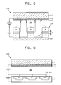
- Figure 5 is a schematic cross-sectional view of a light emitting device 130 using electron emission according to a second embodiment.
- the light emitting device 130 includes a plurality of PN junctions 131, an anode electrode 12, and a phosphor layer 13.
- the light emitting device 130 may further include a first substrate 37 on which the PN junctions 37 are formed, a second substrate 11 on which the anode electrode 12 and the phosphor layer 13 are sequentially formed, and a plurality of spacers (not shown) which maintain the space 35 between the first substrate 37 and the second substrate 11.
- the first substrate 37 and the second substrate 11 may be sealed with glass frit.
- the light emitting device 130 can also generate visible light using the two methods described above.
- Figure 6 is a schematic cross-sectional view of a light emitting device 230 using electron emission according to a third embodiment.
- the light emitting device 230 includes a monocrystalline substrate 231, an anode electrode 12, and a phosphor layer 13.
- the entirety of the monocrystalline substrate 231 is doped with p-type impurities, and PN junctions are formed on a surface of the monocrystalline substrate 231.
- the PN junctions each include a depletion layer 234 having a predetermined thickness, and the depletion layer 234 is formed by diffusing n-type impurities 232 into the surface of the monocrystalline substrate 231.
- the anode electrode 12 is opposite the monocrystalline substrate 231, and the phosphor layer 13 is attached to a surface of the anode electrode 12.
- the light emitting device 230 may further include a front substrate 11 on which the anode electrode 12 and the phosphor layer 13 are sequentially formed, and the thickness of the depletion layer 234 may be from about 1 nm to about 100 nm. Since the n-type impurities 232 are diffused into the surface of the monocrystalline substrate 231, the depletion layer 234 is exposed toward the front substrate 11. Electrons are emitted from the depletion layer 234 and travel toward the anode electrode 12. As described above, these electrons cause visible light to be generated.
- a light emission space 35 is defined by the front substrate 11 and the monocrystalline substrate 231.
- a plurality of spacers may be used, and the front substrate 11 and the monocrystalline substrate 231 may be sealed with glass frit (not shown).
- the light emitting devices 30, 130, and 230 described above may be used as a surface light source of a predetermined size.
- the light emitting device 30, 130, and 230 may be used as a back light unit (BLU), i.e., a surface light source of a liquid crystal display (LCD).
- BLU back light unit
- LCD liquid crystal display
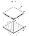
- Figure 7 is a perspective view of a flat display apparatus including a light emitting device using electron emission as a BLU.
- Figure 8 is a cross-sectional view taken along line VIII-VIII of Figure 7.
- Identical names are used for elements of the flat display apparatus illustrated in Figure 7 and 8, which correspond to the elements described above, such as first substrate, a second substrate, and a spacer.
- different reference numerals are used.
- Elements included in an LCD panel 700, which will be described as an example, can be clearly distinguished by reference numerals.
- the flat display apparatus includes the LCD panel 700 as a light receiving/generating display panel and a BLU which supplies light to the LCD panel 700.
- a flexible printed circuit board (FPCB) 720 that transmits an image signal is attached to the LCD 700, and a spacer 730 that maintains a gap between the LCD panel 700 and the BLU disposed at the back of the LCD panel 700.
- FPCB flexible printed circuit board
- the BLU is the light emitting device 130 described above and is supplied with power through a connection cable 104.
- the BLU emits visible light V through the second substrate 11 disposed on a front surface of the light emitting device 130 such that the emitted visible light V can be supplied to the LCD panel 700.
- the light emitting device 130 illustrated in Figure 8 may or may not be identical to the light emitting device 130 illustrated in Figure 5.
- the light emitting device 130 in Figure 8 may include the first substrate 37 and the second substrate 11 which are separated from each other by a predetermined height and form a predetermined space 35 therebetween. Since the configurations of the first and second substrates 37 and 11 and elements installed thereon can be identical to those of the elements of the light emitting device 130 according to the second embodiment, a detailed description thereof will not be repeated.
- electrons are emitted from the depletion layer 34 due to an electric field formed between the n-type semiconductor, the p-type semiconductor and the anode electrode 12. As the emitted electrons collide with the phosphor layer 13, the visible light V is generated. The generated visible light V travels toward the LCD panel 700 disposed in front of the light emitting device 130.
- the LCD panel 700 includes a first substrate 505.
- a buffer layer 510 is formed on the first substrate 505, and a semiconductor layer 580 is formed in a predetermined pattern on the buffer layer 510.
- a first insulating layer 520 is formed on the semiconductor layer 580, a gate electrode 590 is formed in a predetermined pattern on the first insulating layer 520, and a second insulating layer 530 is formed on the gate electrode 590.
- the first and second insulating layers 520 and 530 are etched through an etching process such as a dry-etching process, thereby exposing a portion of the semiconductor layer 580.
- a source electrode 570 and a drain electrode 610 are formed above and extend down to the exposed portion of the semiconductor layer 580.
- a third insulating layer 540 is formed, and a planarization layer 550 is formed on the third insulating layer 540.
- the third insulating layer 540 and a portion of the planarization layer 550 are etched, and the first electrode 620 is formed in a predetermined pattern on the planarization layer 550 such that the drain electrode 610 and the first electrode 620 contact each other.
- a transparent second substrate 680 is manufactured separately from the first substrate 505, and a color filter layer 670 is formed on a bottom surface 680a of the second substrate 680.
- the second electrode 660 is formed on a bottom surface 670a of the color filter layer 670, and a first alignment layer 630 and a second alignment layer 650 which are used to align molecules of liquid crystal in a liquid crystal layer 640 are respectively formed on surfaces of the first and second electrodes 620 and 660 that face each other.
- a first polarizing layer 500 is formed on a bottom surface of the first substrate 505, and a second polarizing layer 690 is formed on a top surface 680b of the second substrate 680.
- a protective film 695 is formed on a top surface 690a of the second polarizing layer 690.
- a spacer 560 that defines the liquid crystal layer 640 is interposed between the color filter layer 670 and the planarization layer 550.
- a potential difference is generated between the first electrode 620 and the second electrode 660 by an external signal which is controlled by the gate electrode 590, the source electrode 570, and the drain electrode 610.
- the potential difference determines the alignment of the liquid crystal layer 640, and the visible light V supplied to the BLU 130 is blocked or transmitted according to the alignment of the liquid crystal layer 640.
- the visible light V that has transmitted through the liquid crystal layer 640 passes through the color filter layer 670, it becomes colored, thereby forming an image.
- the LCD panel 700 is illustrated in Figure 8 as an example.
- a display panel used in the flat display apparatus is not limited thereto. Diverse non-emissive display panels may be used in the flat display apparatus.
- the flat display apparatus which includes the light emitting device using electron emission as a BLU can produce an image with enhanced brightness and have a longer life as a result of an increase in the brightness and lifetime of the BLU.
- the present embodiments provide a light emitting device which can display an image using electron emission.
- the light emitting device can display an image in different ways using a phosphor layer which is formed of a different material according to whether an internal space is maintained in a vacuum state or whether the space is filed with an excitation gas.
- the light emitting device has a structure that allows a nano-sized gap to be easily formed using a depletion layer of a PN junction.
- the light emitting device can operate as follows.
- the space inside the light emitting device is filled with the excitation gas, the excitation gas is excited by electrons, and UV rays are generated by the exited excitation gas.
- the UV rays cause the phosphor layer to generate visible light.
- the light emitting device has far better energy efficiency than a conventional PDP which generates plasma discharge to generate UV rays, excite a phosphor layer using the UV rays, and thus generate visible light.
Landscapes
- Cathode-Ray Tubes And Fluorescent Screens For Display (AREA)
- Luminescent Compositions (AREA)
- Discharge Lamps And Accessories Thereof (AREA)
- Cold Cathode And The Manufacture (AREA)
- Liquid Crystal (AREA)
- Planar Illumination Modules (AREA)
Applications Claiming Priority (1)
| Application Number | Priority Date | Filing Date | Title |
|---|---|---|---|
| KR1020050095487A KR100708717B1 (ko) | 2005-10-11 | 2005-10-11 | 전자 방출 발광 소자 및 이를 이용한 평판 디스플레이 장치 |
Publications (2)
| Publication Number | Publication Date |
|---|---|
| EP1775751A2 true EP1775751A2 (de) | 2007-04-18 |
| EP1775751A3 EP1775751A3 (de) | 2008-07-23 |
Family
ID=37607083
Family Applications (1)
| Application Number | Title | Priority Date | Filing Date |
|---|---|---|---|
| EP06122080A Withdrawn EP1775751A3 (de) | 2005-10-11 | 2006-10-11 | Lichtemitter auf Basis der Elektronenemission und darauf aufbauende Flachanzeigetafel |
Country Status (5)
| Country | Link |
|---|---|
| US (1) | US20070080626A1 (de) |
| EP (1) | EP1775751A3 (de) |
| JP (1) | JP2007109630A (de) |
| KR (1) | KR100708717B1 (de) |
| CN (1) | CN1949434A (de) |
Cited By (2)
| Publication number | Priority date | Publication date | Assignee | Title |
|---|---|---|---|---|
| FR2917191A1 (fr) * | 2007-06-11 | 2008-12-12 | Commissariat Energie Atomique | Dispositif d'eclairage pour ecran a cristal liquide |
| EP2028251A1 (de) * | 2007-08-21 | 2009-02-25 | Samsung SDI Co., Ltd. | Weißer Phosphor, Lichtemissionsvorrichtung damit und Anzeigevorrichtung |
Families Citing this family (7)
| Publication number | Priority date | Publication date | Assignee | Title |
|---|---|---|---|---|
| JP4536077B2 (ja) * | 2007-03-01 | 2010-09-01 | 株式会社沖データ | Ledバックライト装置及び液晶表示装置 |
| JP2008218691A (ja) * | 2007-03-05 | 2008-09-18 | Oki Data Corp | Ledバックライト装置及び液晶表示装置 |
| JP4381439B2 (ja) * | 2007-09-18 | 2009-12-09 | 株式会社沖データ | Ledバックライト装置及び液晶表示装置 |
| US8013952B2 (en) * | 2007-12-25 | 2011-09-06 | Oki Data Corporation | LED backlight device and LCD device |
| JP5129674B2 (ja) * | 2008-07-09 | 2013-01-30 | パナソニック株式会社 | 発光装置 |
| KR101775375B1 (ko) * | 2011-03-29 | 2017-09-06 | 삼성전자주식회사 | 반도체 발광소자 제조방법 및 이에 이용되는 페이스트 도포용 마스크 |
| CN109301045B (zh) * | 2018-10-19 | 2020-07-31 | 京东方科技集团股份有限公司 | 一种发光器件及其制备方法、显示装置 |
Citations (2)
| Publication number | Priority date | Publication date | Assignee | Title |
|---|---|---|---|---|
| DE19802435A1 (de) | 1997-02-05 | 1998-08-06 | Smiths Industries Plc | Elektronenemittervorrichtung |
| US5984752A (en) | 1994-10-05 | 1999-11-16 | Matsushita Electric Industrial Co., Ltd. | Electron emission cathode; an electron emission device, a flat display, a thermoelectric cooling device incorporating the same; and a method for producing the electron emission cathode |
Family Cites Families (15)
| Publication number | Priority date | Publication date | Assignee | Title |
|---|---|---|---|---|
| US4994708A (en) | 1986-07-01 | 1991-02-19 | Canon Kabushiki Kaisha | Cold cathode device |
| US5199918A (en) * | 1991-11-07 | 1993-04-06 | Microelectronics And Computer Technology Corporation | Method of forming field emitter device with diamond emission tips |
| US5404277A (en) * | 1993-02-16 | 1995-04-04 | Lindblad; Edward W. | Apparatus for backlighting LCD |
| US6417605B1 (en) * | 1994-09-16 | 2002-07-09 | Micron Technology, Inc. | Method of preventing junction leakage in field emission devices |
| JPH1050205A (ja) * | 1996-08-01 | 1998-02-20 | Matsushita Electric Ind Co Ltd | 電界放出型電子源及びその製造方法 |
| KR19990034461A (ko) * | 1997-10-29 | 1999-05-15 | 엄길용 | 평판표시소자 |
| KR100354532B1 (ko) * | 1998-02-18 | 2003-01-15 | 삼성전자 주식회사 | 복수방출부 냉음극소자 |
| FR2785719B1 (fr) * | 1998-11-09 | 2001-01-19 | Pixtech Sa | Procede d'encapsulation de luminophores |
| DE10009915A1 (de) * | 2000-03-01 | 2001-09-27 | Philips Corp Intellectual Pty | Plasmabildschirm mit UV-Licht emittierender Schicht |
| DE10045407A1 (de) * | 2000-09-14 | 2002-03-28 | Philips Corp Intellectual Pty | Flüssigkristallbildschirm mit Hintergrundbeleuchtung |
| JP3814527B2 (ja) * | 2000-12-06 | 2006-08-30 | キヤノン株式会社 | 画像表示装置 |
| JP2003157773A (ja) * | 2001-09-07 | 2003-05-30 | Sony Corp | プラズマ表示装置 |
| US6841794B2 (en) * | 2003-02-18 | 2005-01-11 | Hewlett-Packard Development Company, L.P. | Dielectric emitter with PN junction |
| WO2005034164A1 (ja) * | 2003-09-30 | 2005-04-14 | Sumitomo Electric Industries, Ltd. | 電子放出素子 |
| JP4131238B2 (ja) * | 2003-12-26 | 2008-08-13 | ソニー株式会社 | 表示用パネル及び表示装置 |
-
2005
- 2005-10-11 KR KR1020050095487A patent/KR100708717B1/ko not_active Expired - Fee Related
-
2006
- 2006-07-10 JP JP2006189625A patent/JP2007109630A/ja active Pending
- 2006-10-10 US US11/546,456 patent/US20070080626A1/en not_active Abandoned
- 2006-10-11 EP EP06122080A patent/EP1775751A3/de not_active Withdrawn
- 2006-10-11 CN CNA2006101362005A patent/CN1949434A/zh active Pending
Patent Citations (2)
| Publication number | Priority date | Publication date | Assignee | Title |
|---|---|---|---|---|
| US5984752A (en) | 1994-10-05 | 1999-11-16 | Matsushita Electric Industrial Co., Ltd. | Electron emission cathode; an electron emission device, a flat display, a thermoelectric cooling device incorporating the same; and a method for producing the electron emission cathode |
| DE19802435A1 (de) | 1997-02-05 | 1998-08-06 | Smiths Industries Plc | Elektronenemittervorrichtung |
Cited By (5)
| Publication number | Priority date | Publication date | Assignee | Title |
|---|---|---|---|---|
| FR2917191A1 (fr) * | 2007-06-11 | 2008-12-12 | Commissariat Energie Atomique | Dispositif d'eclairage pour ecran a cristal liquide |
| WO2008155215A1 (fr) * | 2007-06-11 | 2008-12-24 | Commissariat A L'energie Atomique | Dispositif d'eclairage pour ecran a cristal liquide |
| US8675150B2 (en) | 2007-06-11 | 2014-03-18 | Commissariat A L'energie Atomique | Lighting device for liquid crystal screen |
| EP2028251A1 (de) * | 2007-08-21 | 2009-02-25 | Samsung SDI Co., Ltd. | Weißer Phosphor, Lichtemissionsvorrichtung damit und Anzeigevorrichtung |
| US7952266B2 (en) | 2007-08-21 | 2011-05-31 | Samsung Sdi Co., Ltd. | White phosphor, light emission device including the same, and display device |
Also Published As
| Publication number | Publication date |
|---|---|
| KR100708717B1 (ko) | 2007-04-17 |
| US20070080626A1 (en) | 2007-04-12 |
| CN1949434A (zh) | 2007-04-18 |
| KR20070040123A (ko) | 2007-04-16 |
| JP2007109630A (ja) | 2007-04-26 |
| EP1775751A3 (de) | 2008-07-23 |
Similar Documents
| Publication | Publication Date | Title |
|---|---|---|
| EP1775751A2 (de) | Lichtemitter auf Basis der Elektronenemission und darauf aufbauende Flachanzeigetafel | |
| EP1814141B1 (de) | Elektronenemissionsvorrichtung, Hintergrundbeleuchtungseinheit (BLU) mit Elektronenemissionsvorrichtung, Flachbildschirm mit BLU und Ansteuerungsverfahren für die Elektronenemissionsvorrichtung | |
| TW200415665A (en) | Flat panel display and method of manufacturing the same | |
| US7923915B2 (en) | Display pixel structure and display apparatus | |
| KR100730165B1 (ko) | 발광 소자 및 이를 이용한 평판 디스플레이 장치 | |
| KR20040027027A (ko) | 백 라이트 유닛과 이를 이용한 액정표시장치 | |
| KR100719563B1 (ko) | 전자 방출 발광 소자 및 이를 이용한 평판 디스플레이 장치 | |
| US20070096660A1 (en) | Display device | |
| JP2007165308A (ja) | 表示装置 | |
| US7462982B2 (en) | Flat panel display using silicon light-emitting device | |
| KR100918871B1 (ko) | 교류 구동형 평면램프 | |
| KR100708716B1 (ko) | 전자 방출 발광 소자, 이를 이용한 평판 디스플레이 장치및 그 제조 방법 | |
| KR100692814B1 (ko) | 플라즈마 디스플레이 패널 | |
| KR100918813B1 (ko) | 선택 영역별 밝기 조절이 가능한 면광원 장치 | |
| KR100333718B1 (ko) | 캐소드루미네슨스형광체를갖는플라즈마디스플레이패널 | |
| US7667233B2 (en) | Display device, flat lamp and method of fabricating the display device and flat lamp | |
| KR100719584B1 (ko) | 표시장치 | |
| KR20060084501A (ko) | 전자기장을 이용한 전계방출소자 및 그 구동방법 | |
| US20070211193A1 (en) | Surface light source device | |
| US20070096630A1 (en) | Field emission backlight unit and its method of operation | |
| KR100777727B1 (ko) | 디스플레이 장치 | |
| KR100673318B1 (ko) | 면분할 구동제어 기능을 갖는 면광원 장치 | |
| KR20070046594A (ko) | 표시 장치 | |
| KR20060102165A (ko) | 평판 발광 램프 |
Legal Events
| Date | Code | Title | Description |
|---|---|---|---|
| PUAI | Public reference made under article 153(3) epc to a published international application that has entered the european phase |
Free format text: ORIGINAL CODE: 0009012 |
|
| 17P | Request for examination filed |
Effective date: 20061011 |
|
| AK | Designated contracting states |
Kind code of ref document: A2 Designated state(s): AT BE BG CH CY CZ DE DK EE ES FI FR GB GR HU IE IS IT LI LT LU LV MC NL PL PT RO SE SI SK TR |
|
| AX | Request for extension of the european patent |
Extension state: AL BA HR MK YU |
|
| PUAL | Search report despatched |
Free format text: ORIGINAL CODE: 0009013 |
|
| AK | Designated contracting states |
Kind code of ref document: A3 Designated state(s): AT BE BG CH CY CZ DE DK EE ES FI FR GB GR HU IE IS IT LI LT LU LV MC NL PL PT RO SE SI SK TR |
|
| AX | Request for extension of the european patent |
Extension state: AL BA HR MK RS |
|
| AKX | Designation fees paid |
Designated state(s): DE FR GB |
|
| RAP1 | Party data changed (applicant data changed or rights of an application transferred) |
Owner name: SAMSUNG SDI CO., LTD. |
|
| STAA | Information on the status of an ep patent application or granted ep patent |
Free format text: STATUS: THE APPLICATION HAS BEEN WITHDRAWN |
|
| 18W | Application withdrawn |
Effective date: 20091106 |