EP1777782B1 - Antenne à large bande avec transformation d'impédance - Google Patents
Antenne à large bande avec transformation d'impédance Download PDFInfo
- Publication number
- EP1777782B1 EP1777782B1 EP06020972A EP06020972A EP1777782B1 EP 1777782 B1 EP1777782 B1 EP 1777782B1 EP 06020972 A EP06020972 A EP 06020972A EP 06020972 A EP06020972 A EP 06020972A EP 1777782 B1 EP1777782 B1 EP 1777782B1
- Authority
- EP
- European Patent Office
- Prior art keywords
- wide band
- feeding
- impedance transformation
- feeding part
- band antenna
- Prior art date
- Legal status (The legal status is an assumption and is not a legal conclusion. Google has not performed a legal analysis and makes no representation as to the accuracy of the status listed.)
- Ceased
Links
- 230000009466 transformation Effects 0.000 title 1
- 230000005855 radiation Effects 0.000 claims description 24
- 239000002356 single layer Substances 0.000 description 3
- 230000009286 beneficial effect Effects 0.000 description 1
- 230000010267 cellular communication Effects 0.000 description 1
- 230000009977 dual effect Effects 0.000 description 1
- 239000010410 layer Substances 0.000 description 1
- 239000000758 substrate Substances 0.000 description 1
Images



Classifications
-
- H—ELECTRICITY
- H01—ELECTRIC ELEMENTS
- H01Q—ANTENNAS, i.e. RADIO AERIALS
- H01Q13/00—Waveguide horns or mouths; Slot antennas; Leaky-waveguide antennas; Equivalent structures causing radiation along the transmission path of a guided wave
-
- H—ELECTRICITY
- H01—ELECTRIC ELEMENTS
- H01Q—ANTENNAS, i.e. RADIO AERIALS
- H01Q9/00—Electrically-short antennas having dimensions not more than twice the operating wavelength and consisting of conductive active radiating elements
- H01Q9/04—Resonant antennas
- H01Q9/0407—Substantially flat resonant element parallel to ground plane, e.g. patch antenna
- H01Q9/0421—Substantially flat resonant element parallel to ground plane, e.g. patch antenna with a shorting wall or a shorting pin at one end of the element
-
- H—ELECTRICITY
- H01—ELECTRIC ELEMENTS
- H01Q—ANTENNAS, i.e. RADIO AERIALS
- H01Q1/00—Details of, or arrangements associated with, antennas
- H01Q1/12—Supports; Mounting means
- H01Q1/22—Supports; Mounting means by structural association with other equipment or articles
- H01Q1/24—Supports; Mounting means by structural association with other equipment or articles with receiving set
-
- H—ELECTRICITY
- H01—ELECTRIC ELEMENTS
- H01Q—ANTENNAS, i.e. RADIO AERIALS
- H01Q1/00—Details of, or arrangements associated with, antennas
- H01Q1/12—Supports; Mounting means
- H01Q1/22—Supports; Mounting means by structural association with other equipment or articles
- H01Q1/24—Supports; Mounting means by structural association with other equipment or articles with receiving set
- H01Q1/241—Supports; Mounting means by structural association with other equipment or articles with receiving set used in mobile communications, e.g. GSM
- H01Q1/242—Supports; Mounting means by structural association with other equipment or articles with receiving set used in mobile communications, e.g. GSM specially adapted for hand-held use
- H01Q1/243—Supports; Mounting means by structural association with other equipment or articles with receiving set used in mobile communications, e.g. GSM specially adapted for hand-held use with built-in antennas
-
- H—ELECTRICITY
- H01—ELECTRIC ELEMENTS
- H01Q—ANTENNAS, i.e. RADIO AERIALS
- H01Q1/00—Details of, or arrangements associated with, antennas
- H01Q1/36—Structural form of radiating elements, e.g. cone, spiral, umbrella; Particular materials used therewith
- H01Q1/38—Structural form of radiating elements, e.g. cone, spiral, umbrella; Particular materials used therewith formed by a conductive layer on an insulating support
-
- H—ELECTRICITY
- H01—ELECTRIC ELEMENTS
- H01Q—ANTENNAS, i.e. RADIO AERIALS
- H01Q5/00—Arrangements for simultaneous operation of antennas on two or more different wavebands, e.g. dual-band or multi-band arrangements
- H01Q5/30—Arrangements for providing operation on different wavebands
- H01Q5/307—Individual or coupled radiating elements, each element being fed in an unspecified way
- H01Q5/342—Individual or coupled radiating elements, each element being fed in an unspecified way for different propagation modes
- H01Q5/357—Individual or coupled radiating elements, each element being fed in an unspecified way for different propagation modes using a single feed point
- H01Q5/364—Creating multiple current paths
- H01Q5/371—Branching current paths
Definitions
- FIG. 1A is a perspective view showing a conventional single layer wide band antenna using stubs
- FIG. 1B is a bottom view of the wide band antenna of FIG. 1A .
- a conventional antenna 10 includes a dielectric(substrate) 20 provided on the upper portion thereof, a patch 40 formed on the dielectric 20 to have a width less than that of the dielectric 20 and to have a hole 30 formed therein, thin plate-shaped conductive stubs 50 attached to the diagonal corners of the patch 40 and operated to transform the resonant frequency and impedance of the antenna 10 by converting the location and size of the conductive stubs 50, and a conductive ground plane 60 attached to the bottom surface of the dielectric 20.
- the antenna 10 includes a coaxial cable 80 that is soldered with a feeding point 70 through a hole 30 formed in the patch 40 and is operated to provide an external signal source to the patch 40.
- the patch 40 having a predetermined size is constructed in such a way that a first stub 50, attached to the upper left portion of the patch 40, and a second stub 50, attached to the lower right portion of the patch 40, are integrated with the patch 40.
- wide band characteristics can be realized only when the locations of the stubs 50 are designed so as to be exactly symmetrical around the center of the patch 40. If the stubs 50 are installed to be opposite each other, wide band characteristics cannot be realized in the antenna 10, and thus the stubs 50 are placed to be approximately symmetrical with each other around the center of the patch 40.
- the dielectric 20, disposed between the ground plane 60 and the patch 40, which is a radiation element, can be filled with an air layer according to the purpose of the antenna 10.
- a connector required to feed the antenna 10 is also placed to be spaced apart from the center of the antenna 10 by a predetermined distance in the direction of one side thereof, so that the impedance of the antenna can be adjusted using the location of the feeding point 70, together with the sizes of the stubs 50, thus obtaining wide band characteristics through impedance matching.
- the conventional single layer wide band antenna using stubs is problematic in that, since the sizes of stubs or the location of a feeding point are changed so as to adjust the impedance thereof, there is a limitation in the space in which the antenna can actually be mounted in a wireless communication terminal, and since a multiple band must also be supported in the same antenna space, it is difficult to utilize such an antenna for a wireless communication system.
- an object of the present invention is to provide an impedance transformation-type wide band antenna, which is beneficial for the miniaturization of the main body thereof.
- the feeding part may be designed so that impedances are matched using a length and interval of the feeding part, which is bent multiple times.
- an inductance is introduced based on a size of the through hole formed in the feeding part, thereby realizing broadband impedance matching.
- the radiation part comprises a first stub for generating low resonant frequencies and a second stub for generating high resonant frequencies according to a terminated length of the stubs.
- FIG. 2A is a perspective view showing the top surface of an impedance transformation-type wide band antenna according to an embodiment of the present invention
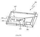
- FIG. 2B is a perspective view showing the bottom surface of the impedance transformation-type wide band antenna according to an embodiment of the present invention.
- a radiation part 240 is made of a metallic plate formed in the shape of a rectangular parallelepiped, and part of one side surface extends, and thus a feeding part 220 and a short circuit part 290 are formed on the bottom surface of the radiation part 240.
- Stubs 250 defined by a plurality of slots 260 formed in the top surface and side surfaces of the radiation part 240 in the shape of a meandering line, are formed both on the top surface and side surfaces of the radiation part 240 to have a predetermined length, and are terminated with one ends thereof opened.
- the stubs 250 are divided into arbitrary shapes by the slots 260, and include a first stub 270 and a second stub 280.
- the feeding part 220 is adjacent to the short circuit part 290, and is formed to extend from the stubs 250 formed on the side surface of the radiation part 240 and to be bent multiple times in a " ⁇ "-shape, and to have a through hole 230 formed therein, thus a multi-path structure is implemented. Further, the feeding part 220 can be formed in a "2"-shape or various shapes within the height limitation.
- the feeding pin 210 is formed on the end of the feeding part 220 in the shape of a rectangle having a predetermined width.
- FIG. 3 is a graph showing the characteristics of the antenna of FIGS. 2A and 2B .
- the graph illustrates Standing Wave Ratio (SWR) characteristics of the antenna 200, and shows wide band characteristics.
- a frequency band for cellular communication which is currently commercialized is a band ranging from 800 MHz to 900 MHz
- a frequency band for Personal Communication Services (PCS) is a band ranging from 1700 MHz to 1900 MHz.
- a frequency band for International Mobile Telecommunications-2000 (IMT-2000) is a band ranging from 1900 MHz to 2200 MHz.
- IMT-2000 International Mobile Telecommunications-2000
- For an actual usage band for IMT-2000, a band of 230 MHz is assigned, and IMT-2000 must be operated in a wide band. If such characteristics are compared to those of the antenna 200 of the present invention, it can be seen that the wide band characteristics of the antenna are sufficiently learned, and the antenna of the present invention is utilized for a dual band or multiple band.
- the antenna of the present invention not only can cover respective bands, but also can be simultaneously used for different frequency bands, as a single antenna, in a wireless communication system that uses different frequency bands.
- the present invention provides an impedance transformation-type wide band antenna, which matches impedances using the length and interval of a feeding part, which is formed in a multi-path structure and is bent multiple times, the vertical distance between a short circuit part connected to an external ground and a radiation part, and the size of a through hole formed in the feeding part, so that a plurality of wide band resonant frequencies is formed, thus enabling the wide band antenna to be simultaneously used for different frequency bands, as a single antenna, in a wireless communication system that uses different frequency bands.
Landscapes
- Engineering & Computer Science (AREA)
- Computer Networks & Wireless Communication (AREA)
- Waveguide Aerials (AREA)
Claims (4)
- Antenne à bande large de type à transformation d'impédance comprenant :une partie de rayonnement (240) formée pour avoir une longueur et une largeur prédéterminées en fonction d'une fréquence de service, la partie de rayonnement incluant une pluralité de rameaux formés sous forme arbitraire en fonction de l'emplacement d'une pluralité de fentes (260) formées dans une surface supérieure et des surfaces latérale de la partie de rayonnement ;une partie de court-circuit (290) pour provoquer la connexion d'une partie d'une surface latérale de la partie de rayonnement (240) à une masse de carte de circuit imprimé externe ;une partie d'alimentation (220) formée par un rameau s'étendant d'un côté de la surface supérieure de la partie de rayonnement (240) pour être adjacent à la partie de court-circuit (290) ;une broche d'alimentation (210) formée à une extrémité de la partie d'alimentation (220) et configurée pour être alimentée en courant ;caractérisée en ce que
ladite partie d'alimentation formée en tant que structure à chemins multiples est courbée de multiples fois en un S et possède un orifice traversant (230) de sorte que la hauteur et la longueur de la partie d'alimentation (220) et la taille de l'orifice traversant (230) sont ajustées pour générer une pluralité de fréquences résonantes. - Antenne à bande large de type à transformation d'impédance selon la revendication 1, dans laquelle une inductance est introduite en fonction de la longueur de la partie d'alimentation (220) et une capacitance est introduite en fonction d'un intervalle de la partie d'alimentation (220) qui est courbé de multiples fois.
- Antenne à bande large de type à transformation d'impédance selon la revendication 2, dans laquelle l'inductance est introduite en fonction d'une taille de l'orifice traversant (230) formé dans la partie d'alimentation (220), réalisant de ce fait une correspondance d'impédance à large bande.
- Antenne à bande large de type à transformation d'impédance selon la revendication 1, dans laquelle la partie de rayonnement (240) comprend un premier rameau (270) pour générer des fréquences résonantes basses et un second rameau (280) pour générer des fréquences résonantes hautes en fonction d'une longueur de terminaison des rameaux.
Applications Claiming Priority (1)
| Application Number | Priority Date | Filing Date | Title |
|---|---|---|---|
| KR1020050099343A KR100735154B1 (ko) | 2005-10-20 | 2005-10-20 | 임피던스 변환형 광대역 안테나 |
Publications (2)
| Publication Number | Publication Date |
|---|---|
| EP1777782A1 EP1777782A1 (fr) | 2007-04-25 |
| EP1777782B1 true EP1777782B1 (fr) | 2012-05-30 |
Family
ID=37671004
Family Applications (1)
| Application Number | Title | Priority Date | Filing Date |
|---|---|---|---|
| EP06020972A Ceased EP1777782B1 (fr) | 2005-10-20 | 2006-10-05 | Antenne à large bande avec transformation d'impédance |
Country Status (3)
| Country | Link |
|---|---|
| US (1) | US7619566B2 (fr) |
| EP (1) | EP1777782B1 (fr) |
| KR (1) | KR100735154B1 (fr) |
Families Citing this family (8)
| Publication number | Priority date | Publication date | Assignee | Title |
|---|---|---|---|---|
| USD612368S1 (en) * | 2009-09-28 | 2010-03-23 | Cheng Uei Precision Industry Co., Ltd. | Double-band antenna |
| CN102104190A (zh) * | 2009-12-21 | 2011-06-22 | 鸿富锦精密工业(深圳)有限公司 | 天线及其小型化方法 |
| USD633901S1 (en) * | 2010-10-27 | 2011-03-08 | Cheng Uei Precision Industry Co., Ltd. | Multi-band antenna |
| WO2012112022A1 (fr) * | 2011-02-18 | 2012-08-23 | Laird Technologies, Inc. | Antennes quart d'onde court-circuitées planes multibandes (antennes pifa), et systèmes à isolement amélioré |
| US10243251B2 (en) * | 2015-07-31 | 2019-03-26 | Agc Automotive Americas R&D, Inc. | Multi-band antenna for a window assembly |
| CN106972243B (zh) * | 2017-01-22 | 2019-05-21 | 中国计量大学 | 一种覆盖gnss的多频段双向共面4g微带天线 |
| CN108666752A (zh) * | 2018-04-17 | 2018-10-16 | 惠州市元盛科技有限公司 | 一种平面天线 |
| CN108990315B (zh) * | 2018-10-12 | 2021-04-06 | 郑州云海信息技术有限公司 | 一种差分过孔阻抗控制方法 |
Family Cites Families (10)
| Publication number | Priority date | Publication date | Assignee | Title |
|---|---|---|---|---|
| FI112723B (fi) * | 1997-03-27 | 2003-12-31 | Nokia Corp | Langattomien viestimien antenni |
| FI113212B (fi) * | 1997-07-08 | 2004-03-15 | Nokia Corp | Usean taajuusalueen kaksoisresonanssiantennirakenne |
| DE10052909A1 (de) * | 2000-10-25 | 2002-05-08 | Siemens Ag | Kommunikationsendgerät |
| KR100423395B1 (ko) * | 2001-07-02 | 2004-03-18 | 삼성전기주식회사 | 칩 안테나 |
| TW529779U (en) * | 2001-10-26 | 2003-04-21 | Hon Hai Prec Ind Co Ltd | Multi-frequency antenna |
| EP1372213A1 (fr) * | 2002-06-11 | 2003-12-17 | Industrial Technology Research Institute | Antenne multibande |
| CN1695268A (zh) * | 2002-11-28 | 2005-11-09 | 捷讯研究有限公司 | 具有贴片和隙缝结构的多频带天线 |
| ES2305321T3 (es) * | 2002-12-06 | 2008-11-01 | Research In Motion Limited | Antena multibanda con estructura de ranura compartida. |
| US7102573B2 (en) * | 2003-01-13 | 2006-09-05 | Cushcraft Corporation | Patch antenna |
| JP4623272B2 (ja) * | 2004-09-02 | 2011-02-02 | ミツミ電機株式会社 | アンテナ装置 |
-
2005
- 2005-10-20 KR KR1020050099343A patent/KR100735154B1/ko not_active Expired - Fee Related
-
2006
- 2006-10-05 EP EP06020972A patent/EP1777782B1/fr not_active Ceased
- 2006-10-20 US US11/551,398 patent/US7619566B2/en not_active Expired - Fee Related
Also Published As
| Publication number | Publication date |
|---|---|
| KR20070043274A (ko) | 2007-04-25 |
| KR100735154B1 (ko) | 2007-07-04 |
| EP1777782A1 (fr) | 2007-04-25 |
| US20070091000A1 (en) | 2007-04-26 |
| US7619566B2 (en) | 2009-11-17 |
Similar Documents
| Publication | Publication Date | Title |
|---|---|---|
| US7564413B2 (en) | Multi-band antenna and mobile communication terminal having the same | |
| US7791541B2 (en) | Printed circuit board | |
| US7333067B2 (en) | Multi-band antenna with wide bandwidth | |
| US6404394B1 (en) | Dual polarization slot antenna assembly | |
| KR101031052B1 (ko) | 멀티밴드 안테나 컴포넌트 | |
| US6677909B2 (en) | Dual band slot antenna with single feed line | |
| US7956812B2 (en) | Wide-band antenna and manufacturing method thereof | |
| US7193576B2 (en) | Ultra wideband bow-tie slot antenna | |
| JP2003163528A (ja) | プリント回路板、表面実装装置アンテナ及び通信装置 | |
| CN1886863A (zh) | 内部多频带天线 | |
| US7230573B2 (en) | Dual-band antenna with an impedance transformer | |
| US9368858B2 (en) | Internal LC antenna for wireless communication device | |
| WO2000052783A1 (fr) | Antenne a large bande d'un circuit d'adaptation et element radiant sur plaque de masse | |
| EP1777782B1 (fr) | Antenne à large bande avec transformation d'impédance | |
| US8284116B2 (en) | Antenna apparatus for internal impedance matching | |
| US7855686B2 (en) | Compact antennas for ultra-wideband applications | |
| KR20020065811A (ko) | 전자결합 인쇄 슬롯 마이크로스트립 안테나 | |
| US20060290571A1 (en) | Ultra wide bandwidth planar antenna | |
| WO2002087012A1 (fr) | Antenne pifa a structure de plan de sol a haute impedance higp | |
| KR20020091760A (ko) | 휴대용 단말기의 내장형 안테나 | |
| JP2002319809A (ja) | アンテナ装置 | |
| US8159400B2 (en) | Chip antenna and mobile-communication terminal having the same | |
| CN2906951Y (zh) | 采用回型振子的三频pcb天线 | |
| KR100723682B1 (ko) | 단말기용 삼중대역 cpw급전 평면 역f형 안테나 | |
| CN2906952Y (zh) | 采用回型振子的双频pcb天线 |
Legal Events
| Date | Code | Title | Description |
|---|---|---|---|
| PUAI | Public reference made under article 153(3) epc to a published international application that has entered the european phase |
Free format text: ORIGINAL CODE: 0009012 |
|
| AK | Designated contracting states |
Kind code of ref document: A1 Designated state(s): AT BE BG CH CY CZ DE DK EE ES FI FR GB GR HU IE IS IT LI LT LU LV MC NL PL PT RO SE SI SK TR |
|
| AX | Request for extension of the european patent |
Extension state: AL BA HR MK YU |
|
| 17P | Request for examination filed |
Effective date: 20070920 |
|
| 17Q | First examination report despatched |
Effective date: 20071025 |
|
| AKX | Designation fees paid |
Designated state(s): DE DK FI FR GB SE |
|
| RAP1 | Party data changed (applicant data changed or rights of an application transferred) |
Owner name: ACE ANTENNA CORP. |
|
| GRAP | Despatch of communication of intention to grant a patent |
Free format text: ORIGINAL CODE: EPIDOSNIGR1 |
|
| GRAS | Grant fee paid |
Free format text: ORIGINAL CODE: EPIDOSNIGR3 |
|
| GRAA | (expected) grant |
Free format text: ORIGINAL CODE: 0009210 |
|
| AK | Designated contracting states |
Kind code of ref document: B1 Designated state(s): DE DK FI FR GB SE |
|
| REG | Reference to a national code |
Ref country code: GB Ref legal event code: FG4D |
|
| REG | Reference to a national code |
Ref country code: DE Ref legal event code: R096 Ref document number: 602006029765 Country of ref document: DE Effective date: 20120726 |
|
| PG25 | Lapsed in a contracting state [announced via postgrant information from national office to epo] |
Ref country code: SE Free format text: LAPSE BECAUSE OF FAILURE TO SUBMIT A TRANSLATION OF THE DESCRIPTION OR TO PAY THE FEE WITHIN THE PRESCRIBED TIME-LIMIT Effective date: 20120530 Ref country code: FI Free format text: LAPSE BECAUSE OF FAILURE TO SUBMIT A TRANSLATION OF THE DESCRIPTION OR TO PAY THE FEE WITHIN THE PRESCRIBED TIME-LIMIT Effective date: 20120530 |
|
| PG25 | Lapsed in a contracting state [announced via postgrant information from national office to epo] |
Ref country code: DK Free format text: LAPSE BECAUSE OF FAILURE TO SUBMIT A TRANSLATION OF THE DESCRIPTION OR TO PAY THE FEE WITHIN THE PRESCRIBED TIME-LIMIT Effective date: 20120530 |
|
| PLBE | No opposition filed within time limit |
Free format text: ORIGINAL CODE: 0009261 |
|
| STAA | Information on the status of an ep patent application or granted ep patent |
Free format text: STATUS: NO OPPOSITION FILED WITHIN TIME LIMIT |
|
| 26N | No opposition filed |
Effective date: 20130301 |
|
| REG | Reference to a national code |
Ref country code: DE Ref legal event code: R097 Ref document number: 602006029765 Country of ref document: DE Effective date: 20130301 |
|
| REG | Reference to a national code |
Ref country code: FR Ref legal event code: PLFP Year of fee payment: 10 |
|
| REG | Reference to a national code |
Ref country code: FR Ref legal event code: PLFP Year of fee payment: 11 |
|
| REG | Reference to a national code |
Ref country code: FR Ref legal event code: PLFP Year of fee payment: 12 |
|
| PGFP | Annual fee paid to national office [announced via postgrant information from national office to epo] |
Ref country code: FR Payment date: 20171010 Year of fee payment: 12 Ref country code: DE Payment date: 20171002 Year of fee payment: 12 |
|
| PGFP | Annual fee paid to national office [announced via postgrant information from national office to epo] |
Ref country code: GB Payment date: 20171002 Year of fee payment: 12 |
|
| REG | Reference to a national code |
Ref country code: DE Ref legal event code: R119 Ref document number: 602006029765 Country of ref document: DE |
|
| GBPC | Gb: european patent ceased through non-payment of renewal fee |
Effective date: 20181005 |
|
| PG25 | Lapsed in a contracting state [announced via postgrant information from national office to epo] |
Ref country code: DE Free format text: LAPSE BECAUSE OF NON-PAYMENT OF DUE FEES Effective date: 20190501 |
|
| PG25 | Lapsed in a contracting state [announced via postgrant information from national office to epo] |
Ref country code: FR Free format text: LAPSE BECAUSE OF NON-PAYMENT OF DUE FEES Effective date: 20181031 |
|
| PG25 | Lapsed in a contracting state [announced via postgrant information from national office to epo] |
Ref country code: GB Free format text: LAPSE BECAUSE OF NON-PAYMENT OF DUE FEES Effective date: 20181005 |