EP1780557A2 - Appareil de diagnostic en médecine nucléaire, appareil de tomographie à émission de positrons et unités de détection - Google Patents
Appareil de diagnostic en médecine nucléaire, appareil de tomographie à émission de positrons et unités de détection Download PDFInfo
- Publication number
- EP1780557A2 EP1780557A2 EP06020152A EP06020152A EP1780557A2 EP 1780557 A2 EP1780557 A2 EP 1780557A2 EP 06020152 A EP06020152 A EP 06020152A EP 06020152 A EP06020152 A EP 06020152A EP 1780557 A2 EP1780557 A2 EP 1780557A2
- Authority
- EP
- European Patent Office
- Prior art keywords
- region
- housing member
- radiation detectors
- signal processors
- coolant
- Prior art date
- Legal status (The legal status is an assumption and is not a legal conclusion. Google has not performed a legal analysis and makes no representation as to the accuracy of the status listed.)
- Withdrawn
Links
- 238000009206 nuclear medicine Methods 0.000 title claims abstract description 28
- 238000002591 computed tomography Methods 0.000 title description 4
- 230000005855 radiation Effects 0.000 claims abstract description 81
- 238000009423 ventilation Methods 0.000 claims abstract description 51
- 239000000428 dust Substances 0.000 claims abstract description 44
- 239000000758 substrate Substances 0.000 claims description 117
- 238000001514 detection method Methods 0.000 claims description 29
- 239000002826 coolant Substances 0.000 claims description 28
- 238000007599 discharging Methods 0.000 claims description 19
- 239000004065 semiconductor Substances 0.000 claims description 13
- 238000000638 solvent extraction Methods 0.000 claims description 9
- 239000000463 material Substances 0.000 claims description 8
- 230000003287 optical effect Effects 0.000 claims description 7
- 238000002600 positron emission tomography Methods 0.000 claims 1
- 238000001816 cooling Methods 0.000 abstract description 24
- 230000000694 effects Effects 0.000 abstract description 4
- 230000002708 enhancing effect Effects 0.000 abstract 1
- 230000005251 gamma ray Effects 0.000 description 24
- 230000008878 coupling Effects 0.000 description 23
- 238000010168 coupling process Methods 0.000 description 23
- 238000005859 coupling reaction Methods 0.000 description 23
- 238000000034 method Methods 0.000 description 12
- 238000002603 single-photon emission computed tomography Methods 0.000 description 11
- 238000012423 maintenance Methods 0.000 description 6
- 230000002285 radioactive effect Effects 0.000 description 6
- 238000010276 construction Methods 0.000 description 5
- MARUHZGHZWCEQU-UHFFFAOYSA-N 5-phenyl-2h-tetrazole Chemical compound C1=CC=CC=C1C1=NNN=N1 MARUHZGHZWCEQU-UHFFFAOYSA-N 0.000 description 3
- 206010028980 Neoplasm Diseases 0.000 description 3
- 238000004140 cleaning Methods 0.000 description 3
- 230000007423 decrease Effects 0.000 description 3
- 238000003745 diagnosis Methods 0.000 description 3
- 239000000945 filler Substances 0.000 description 3
- 238000003384 imaging method Methods 0.000 description 3
- 238000009434 installation Methods 0.000 description 3
- 238000005259 measurement Methods 0.000 description 3
- 239000002245 particle Substances 0.000 description 3
- 230000002093 peripheral effect Effects 0.000 description 3
- BASFCYQUMIYNBI-UHFFFAOYSA-N platinum Chemical compound [Pt] BASFCYQUMIYNBI-UHFFFAOYSA-N 0.000 description 3
- 238000012545 processing Methods 0.000 description 3
- 230000035945 sensitivity Effects 0.000 description 3
- CEGXZKXILQSJHO-KODRXGBYSA-N (3r,4s,5r)-3,4,5,6-tetrahydroxyhexanoyl fluoride Chemical compound OC[C@@H](O)[C@@H](O)[C@H](O)CC(F)=O CEGXZKXILQSJHO-KODRXGBYSA-N 0.000 description 2
- 229910000838 Al alloy Inorganic materials 0.000 description 2
- JOYRKODLDBILNP-UHFFFAOYSA-N Ethyl urethane Chemical compound CCOC(N)=O JOYRKODLDBILNP-UHFFFAOYSA-N 0.000 description 2
- 230000002159 abnormal effect Effects 0.000 description 2
- 238000004378 air conditioning Methods 0.000 description 2
- 229910052782 aluminium Inorganic materials 0.000 description 2
- XAGFODPZIPBFFR-UHFFFAOYSA-N aluminium Chemical compound [Al] XAGFODPZIPBFFR-UHFFFAOYSA-N 0.000 description 2
- 238000006243 chemical reaction Methods 0.000 description 2
- 230000002542 deteriorative effect Effects 0.000 description 2
- 239000003814 drug Substances 0.000 description 2
- 239000010931 gold Substances 0.000 description 2
- 238000007689 inspection Methods 0.000 description 2
- 230000003993 interaction Effects 0.000 description 2
- 238000012986 modification Methods 0.000 description 2
- 230000004048 modification Effects 0.000 description 2
- 230000011218 segmentation Effects 0.000 description 2
- JBRZTFJDHDCESZ-UHFFFAOYSA-N AsGa Chemical compound [As]#[Ga] JBRZTFJDHDCESZ-UHFFFAOYSA-N 0.000 description 1
- 241000282412 Homo Species 0.000 description 1
- 230000005856 abnormality Effects 0.000 description 1
- 230000015572 biosynthetic process Effects 0.000 description 1
- 201000011510 cancer Diseases 0.000 description 1
- 239000003990 capacitor Substances 0.000 description 1
- 239000004020 conductor Substances 0.000 description 1
- 239000000470 constituent Substances 0.000 description 1
- 238000007796 conventional method Methods 0.000 description 1
- 230000001419 dependent effect Effects 0.000 description 1
- 230000006866 deterioration Effects 0.000 description 1
- 238000011161 development Methods 0.000 description 1
- 230000018109 developmental process Effects 0.000 description 1
- 238000005516 engineering process Methods 0.000 description 1
- 239000004744 fabric Substances 0.000 description 1
- -1 for example Substances 0.000 description 1
- 230000005714 functional activity Effects 0.000 description 1
- 230000004153 glucose metabolism Effects 0.000 description 1
- PCHJSUWPFVWCPO-UHFFFAOYSA-N gold Chemical compound [Au] PCHJSUWPFVWCPO-UHFFFAOYSA-N 0.000 description 1
- 229910052737 gold Inorganic materials 0.000 description 1
- 230000006872 improvement Effects 0.000 description 1
- 229910052738 indium Inorganic materials 0.000 description 1
- APFVFJFRJDLVQX-UHFFFAOYSA-N indium atom Chemical compound [In] APFVFJFRJDLVQX-UHFFFAOYSA-N 0.000 description 1
- 239000010410 layer Substances 0.000 description 1
- 239000011159 matrix material Substances 0.000 description 1
- 230000004060 metabolic process Effects 0.000 description 1
- 239000011295 pitch Substances 0.000 description 1
- 229910052697 platinum Inorganic materials 0.000 description 1
- 230000008569 process Effects 0.000 description 1
- 230000000644 propagated effect Effects 0.000 description 1
- 230000001902 propagating effect Effects 0.000 description 1
- 239000012858 resilient material Substances 0.000 description 1
- 238000007789 sealing Methods 0.000 description 1
- 239000002356 single layer Substances 0.000 description 1
- PGAPATLGJSQQBU-UHFFFAOYSA-M thallium(i) bromide Chemical compound [Tl]Br PGAPATLGJSQQBU-UHFFFAOYSA-M 0.000 description 1
- 238000012546 transfer Methods 0.000 description 1
Images


Classifications
-
- G—PHYSICS
- G01—MEASURING; TESTING
- G01T—MEASUREMENT OF NUCLEAR OR X-RADIATION
- G01T1/00—Measuring X-radiation, gamma radiation, corpuscular radiation, or cosmic radiation
- G01T1/29—Measurement performed on radiation beams, e.g. position or section of the beam; Measurement of spatial distribution of radiation
- G01T1/2914—Measurement of spatial distribution of radiation
- G01T1/2985—In depth localisation, e.g. using positron emitters; Tomographic imaging (longitudinal and transverse section imaging; apparatus for radiation diagnosis sequentially in different planes, steroscopic radiation diagnosis)
-
- A—HUMAN NECESSITIES
- A61—MEDICAL OR VETERINARY SCIENCE; HYGIENE
- A61B—DIAGNOSIS; SURGERY; IDENTIFICATION
- A61B6/00—Apparatus or devices for radiation diagnosis; Apparatus or devices for radiation diagnosis combined with radiation therapy equipment
- A61B6/02—Arrangements for diagnosis sequentially in different planes; Stereoscopic radiation diagnosis
- A61B6/03—Computed tomography [CT]
- A61B6/037—Emission tomography
Definitions
- the present invention relates generally to nuclear medicine diagnostic apparatuses that use radiation. More particularly, the invention concerns a nuclear medicine diagnostic apparatus, positron emission computed tomography (PET) apparatus, and detector unit group suitable for performing multiple types of radiation examinations such as X-ray CT, PET, and single-photon emission computed tomography (SPECT).
- PET positron emission computed tomography
- SPECT single-photon emission computed tomography
- the examination techniques that use radiation can be used to examine the insides of target bodies in a non-invasive fashion.
- Radiation examination techniques for human bodies include, for example, X-ray CT, PET, and SPECT. All these techniques are intended to acquire images by measuring the physical quantities of a body to be examined, as integral data of radiation in the emission direction thereof, then back-projecting the integral data, and calculating the physical quantities of individual voxels within the target body.
- These techniques require processing vast volumes of data, and the rapid development of computer technology in recent years has enabled techniques to provide detailed images rapidly and at high resolution.
- the PET and SPECT apparatuses used for diagnosis in nuclear medicine employ a technique that allows detection of the functional activity and metabolism at a molecular biological level that are not detectible with other diagnostic apparatuses such as an X-ray CT apparatus.
- the PET and SPECT apparatuses can provide functional images of target bodies, such as human bodies.
- PET is a technique for acquiring images by administering to humans radioactive pharmaceuticals labeled with a positron emission nuclide such as 18 F, 15 O, or 11 C, and measuring the distribution of the pharmaceutical.
- a positron emission nuclide such as 18 F, 15 O, or 11 C
- the types of pharmaceuticals used include, for example, 2-[F-18] fluoro-2-deoxy-D-glucose ( 18 FDG), which is used to identify a tumor site by utilizing the characteristic that the pharmaceutical densely accumulates at the tumor tissue by means of glucose metabolism.
- the radionuclide that has been introduced into the human body decays and emits a positron ( ⁇ +). Upon combining with an electron and decaying, the emitted positron itself emits one pair of annihilations (annihilation pair) having an energy of 511 keV.
- projection data can be obtained by simultaneously detecting the annihilations using multiple radiation detectors arranged around the target body, and storing radial data thereof.
- Back-projection of the projection data by using a filtered back-projection method, or the like, makes it possible to identify radiation positions, that is, the accumulating positions of the radionuclide.
- SPECT is a technique for acquiring images by administering to target bodies, such as human bodies, a radioactive pharmaceutical labeled with a single-photon emission nuclide, and measuring the distribution of the pharmaceutical.
- a single ⁇ -ray with an energy of about 100 keV is emitted from the pharmaceutical, and the energy of the emitted single ⁇ -ray is measured using a radiation detector.
- the emission direction of the single ⁇ -ray cannot be identified from its energy data measurements.
- SPECT therefore, a collimator is inserted in front of a radiation detector and the single ⁇ -ray is detected only from a specific direction, whereby projection data can be obtained.
- SPECT uses filtered back-projection or the like to obtain image data by back-projection of projection data.
- SPECT differs from PET in that because of energy measurement of the single ⁇ -ray, simultaneous measurement is unnecessary, and hence in that the number of radiation detectors required is small.
- SPECT is also simple in apparatus configuration.
- the above-described conventional PET, SPECT, and other nuclear medicine diagnostic apparatuses use a scintillator(s) as a radiation detector(s) to obtain an image.
- the scintillator requires converting an incident into visible light and then reconverting the light into an electrical signal via a photomultiplier.
- the scintillator has also had a problem in that since the number of photons generated during the conversion into visible light is small and since, as described above, two conversion process steps are necessary, energy resolution decreases and this does not always make diagnosing accuracy improvable. This decrease in energy resolution results in quantitative assessment being impossible, particularly during 3D imaging with PET. This is because the decrease in energy resolution necessitates the energy threshold level of the single ⁇ -ray to be correspondingly reduced and because this results in detection of a large quantity of human body internal scattering which increases noise during 3D imaging.
- semiconductor radiation detectors are attracting attention as radiation detectors for use with nuclear medicine diagnostic apparatuses.
- the semiconductor radiation detectors convert an incident ⁇ -ray directly into an electrical signal, and feature high energy resolution since a large number of electrons and hole pairs are generated.
- the characteristics of these radiation detectors are typically temperature-dependent.
- the characteristics referred to here include time resolution and energy resolution. It is known that these characteristics improve during the use of the radiation detectors under low-temperature conditions.
- Japanese Patent Laid-open No. 2005-128000 (Paragraphs 0058-0060) describes a cooling structure that efficiently cools signal processors and radiation detectors. Maintaining these radiation detectors at low temperature allows the improvement of both image quality and quantitative characteristics, and hence, more accurate diagnosis.
- moisture-proofing and dust-proofing capabilities are important in radiation detectors.
- Semiconductor detectors in particular, need to be applied with a high-voltage bias. If dust sticks to the detector or the high-voltage sections of its circuit board, the dust increases current leakage and reduces energy resolution and time resolution. In addition, an increase in humidity under such a dusty state further reduces energy resolution and time resolution.
- An object of the present invention is to provide the following: a nuclear medicine diagnostic apparatus and positron emission computed tomography apparatus that can, while cooling radiation detectors efficiently, enhance moisture-proofing and dust-proofing effects of radiation detectors without deteriorating maintainability, and achieve highly accurate diagnosis by improving time resolution and energy resolution; and detector units used with the nuclear medicine diagnostic apparatus and the positron emission computed tomography apparatus.
- a nuclear medicine diagnostic apparatus of the present invention has detector units arranged around a bed on which the human body to be examined is to be held, wherein each of the detector units includes: a plurality of unit substrates each further including a plurality of radiation detectors for detecting radiation, and a plurality of signal processors to each of which an independent detection signal from each of the radiation detectors is input; a housing member having the plurality of unit substrates and segmented into a first region in which the plurality of radiation detectors are disposed, and a second region in which the plurality of signal processors are disposed; and coolant discharging means for introducing a gaseous coolant into the second region in order to cool the plurality of signal processors and discharging the coolant from the second region; the housing member being formed with a ventilation hole to communicate with an exterior of the housing member as well as with the first region, and having an anti-dust filter connected to the ventilation hole.
- the nuclear medicine diagnostic apparatus of the present invention is constructed so that each radiation detector is separated from each signal processor and so that while the signal processor is being air-cooled, the radiation detector is ventilated by the ventilation hole having an anti-dust filter.
- the coolant discharging means is contributive for the radiation detector to suppress heat propagation from the signal processor, a heat-generating element, and thus to suppress a temperature rise of the radiation detector itself.
- ventilation holes that enable inflow of air are provided in a section which communicates with the first region in which the radiation detector is provided, and the anti-dust filter is connected to the ventilation holes, thus preventing a flow of dust into the radiation detector.
- the provision of the ventilation holes having the anti-dust filter facilitates humidity control since humidity is immediately set to a value that has been set from the outside of the apparatus.
- the detector unit is used for radiation examination and has the following: a plurality of substrates each including a plurality of radiation detectors for detecting radiation, and a plurality of signal processors to each of which an independent detection signal from each of the radiation detectors is input, a housing member internally having the plurality of substrates, the housing member being segmented into a first region in which the plurality of radiation detectors are disposed, and a second region in which the plurality of signal processors are disposed, a ventilation hole of the second region, which introduces a gaseous coolant into the second region in order to cool the plurality of signal processors and a ventilation port of the first region, communicates with an exterior of the housing member as well as with the first region.
- a nuclear medicine diagnostic apparatus according to a preferred embodiment of the present invention will be described hereunder with reference to Figs. 1 to 5.
- the nuclear medicine diagnostic apparatus of the present embodiment will be described taking a PET apparatus as an example, the present invention is not limited to the PET apparatus and can be applied to other nuclear medicine diagnostic apparatuses such as a SPECT apparatus.
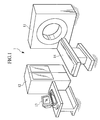
- PET apparatus 1 includes an image acquisition device 11, a data processor 12 which processes detection data obtained by the image acquisition device 11 during imaging and converts the detection data into image data, a display device 13 which makes a two-dimensional or three-dimensional display of the image data that the data processor 12 outputs, and a bed 14 on which to rest a human body (patient) as a human subject H of examination so as to be movable forward and backward in an body-axis direction.
- the image acquisition device 11 includes a detector unit 2 having a large number of semiconductor radiation detectors 21 (hereinafter, referred to simply as detectors, details of which will described later herein).
- This detector unit 2 is disposed inside a casing 11A of the image acquisition device 11, and the detector unit 2 is disposed in large numbers circumferentially with body axis Z of the human subject H as a center so as to encircle the bed 14 that has been inserted into a space S of the image acquisition device 11.
- a radioactive pharmaceutical for example, a fluoro-2-deoxy-D-glucose (FDG) that contains 18 F whose half-life is 110 minutes is administered to the human subject H.
- FDG fluoro-2-deoxy-D-glucose
- This radioactive pharmaceutical accumulates in a cancer-affected region C, for example.
- one pair of ⁇ -rays (radioactive rays) generated during annihilation of the positron emitted from the FDG are simultaneously emitted from the body interior of the human subject H, in angle directions of 180 ⁇ 0.6 degrees. These ⁇ -rays are detected by two detectors 21 positioned in a 180°-shifted condition in opposite directions.
- a position from which the ⁇ -rays have originated (i.e., the accumulating section of the radioactive pharmaceutical) in the body of the human subject H is identified from the detection signals output from the detectors 21.
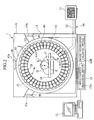
- the configuration of the detector units 2 and peripheral sections thereof, shown in Fig. 2, is schematically shown to illustrate their arrangement. Their detailed construction will be described later.
- the image acquisition device 11 also includes a cooler 50, part of its constituent elements is shown in Fig. 2.
- the cooler 50 cools each detector unit 2, and in the present embodiment, air is used for cooling (gaseous coolant). Details of the cooler 50 will be described later.
- the data processor 12 includes a simultaneous measuring device 12A and an image information creating device 12B.
- the data processor 12 acquires packet data (described later) that is output from an integrated FPGA (Field-Programmable Gate Array) 28 on a coupling substrate 22 built into each detector unit 21 detailed later herein (see Fig. 3B for the packet data and the FPGA 28).
- the simultaneous measuring device 12A identifies the position of the same originating source of the paired ⁇ -rays, only from ⁇ -ray information among all acquired data, and stores the position information into a storage device not shown.
- the image information creating device 12B creates PET image information (tomographic image information) of the human subject H from the identified position information and displays the PET image information on the display device 13.
- the simultaneous measuring device 12A compares ⁇ -ray detection time between plural sets of detection data and judges any two sets of data having a simultaneous measuring time window length of, for example, 10 nanoseconds (ns) or less, as an effective data pair.
- the image information creating device 12B accumulates emission direction data of the ⁇ -ray pair from IDs of the detectors 21 of the effective data pair and then creates a PET image from the emission direction data by image reconstruction. The created PET image is then output to the display device 13.
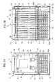
- each detector unit 2 includes a housing member 5, a coolant discharging element 6, an adiabatic member (partitioning member) 7, and unit substrates 20.
- the image acquisition device 11 shown in Fig. 2 is constructed to have, for example, 60 to 70 detector units 2 removably arranged in a circumferential direction of the device 11, which facilitates maintenance and inspection.
- the unit substrates 20 each include a detector substrate 20A that operates as a first substrate, and multiple detectors 21, and the detectors 21 are arranged in matrix form on both sides of the detector substrate 20A.
- detector substrates 20A are arranged inside a housing member 5, in a direction of the body axis Z of the human subject H (i.e., a longitudinal direction of the bed 14) shown in Fig. 2.
- a direction of the body axis Z of the human subject H i.e., a longitudinal direction of the bed 14
- 15 detector substrates 20A in all are provided by way of example.
- the image acquisition device 11 has a total of 64 detectors 21 per side of each detector substrate 20A, 16 units in the circumferential direction of the device 11 (i.e., a layout direction of the detector units 2) and 4 rows in a radial direction of the device 11 (i.e., a direction orthogonal to the layout direction of the detector units 2).
- the detectors 21 are arranged circumferentially around a central axis of the image acquisition device 11 (almost coaxially with the body axis Z of the human subject H).
- the detectors 21 in the present embodiment are arranged densely at small layout pitches to implement high-density mounting of the detectors 21 on the detector substrates 20A. This arrangement makes it possible to improve ⁇ -ray detection efficiency on the detector substrates 20A and reduce an examination time.
- the detectors 21 each have a semiconductor member stacked in a sandwiched condition between a cathode and anode not shown.
- This semiconductor member is constructed of a monocrystal of either cadmium telluride (CdTe), thallium bromide (TlBr), gallium arsenide (GaAs), or the like.
- the anode and the cathode use either platinum (Pt), gold (Au), indium (In), or the like, as their material(s).
- Employing the thus-constructed detectors 21 makes it possible to enhance electrical-charge collection efficiency and to increase a semiconductor member - ⁇ -ray interaction (i.e., a numerical count) for increased sensitivity by reducing the quantity of ⁇ -rays passing through.
- the detectors 21 do not always need to have such a stacked structure and may have a single-layer structure or any other appropriate layer structure.
- the detectors 21 are densely arranged as described above, and as shown in Fig. 5, the detectors 21 are preferably arranged in close proximity to one another in a circumferential direction in the casing 11A (see Figs. 2 and 5) of the image acquisition device 11. By adopting such a structure, it is possible to enhance position resolution of the image obtained.
- each detector 21 detects the 511-keV ⁇ -ray (radiation) used in the PET apparatus 1, and outputs an analog signal ( ⁇ -ray detection signal) associated with an energy of the ⁇ -ray (i.e., the energy that has caused the interaction with respect to the semiconductor member).
- signal processor substrates 20B each have a substrate connector C2 at one end (upper end), and each of the signal processor substrates 20B and the coupling substrates 22 are electrically connected using an interconnecting line R1 connected via the substrate connector C2.
- Integrated circuits for processing the ⁇ -ray detection signals that have been output from each detector 21 described above are mounted on each signal processor substrate 20B.
- the analog ASICs 24 function as signal processors in the present embodiment.
- One analog ASIC 24 includes 32 sets of analog signal processor circuits (analog signal processors), these circuits each having a slow system and a fast system. Independent analog signal processor circuits are provided for each detector 21, and one analog signal processor circuit is connected to one detector 21.
- the fast system includes a timing pick-off circuit that outputs a timing signal for identifying ⁇ -ray detection time of day.
- the slow system has a polarity amplifier (linear amplifier), a band-pass filter (waveform shaper), and a peak hold circuit (wave peak value hold device), which are connected in that order in the system in order to calculate a wave peak value of the detected ⁇ -ray.
- the slow system is named “slow” because the system needs a certain amount of processing time to calculate a wave peak value.
- the ⁇ -ray detection signal that has been output from the detector 21 and passed through a capacitor and a resistor is amplified by a charge amplifier and the polarity amplifier.
- the amplified detection signal is input to the peak hold circuit via the band-pass filter.
- the peak hold circuit holds a maximum value of detection signals, namely, a wave peak value of a ⁇ -ray detection signal proportional to the energy of the detected ⁇ -ray.
- One analog ASIC 24 is an LSI constructed of 32 sets of analog signal processor circuits.
- These integrated circuits amplify the very weak ⁇ -ray detection signal output from the detector 21, and measure the energy of the detected ⁇ -ray and the detection time of day.
- An independent detector ID that has been set for the particular detector 21 beforehand is added to measured energy and detection time data, and the measured energy and detection time data is output as packet data (digital data).
- Each signal processor substrate 20B described above has a connector C1 at the other end (lower end), and the signal processor substrate 20B is mechanically and electrically connected to the above-described detector substrate 20A via the connector C1.
- the detector substrate 20A and the signal processor substrate 20B may be removably coupled with each other by means of a screw (not shown), at an overlapping section between both substrates 20A and 20B. Signals from the detector substrate 20A to the signal processor substrate 20B can be transmitted with minimum loss by using the electrical connection structure of the substrates 20A and 20B. Reduced signal loss improves, for example, energy resolution of the detector 21.
- the detector substrate 20A and the signal processor substrate 20B are interconnected via the connector C1 in this way, these substrates can easily be removed and remounted independently of each other. This means, therefore, that for example, if an abnormality occurs in either detector 21, either analog ASIC 24, or the like, only the abnormal section, that is, only the detector substrate 20A or the signal processor substrate 20B needs to be replaced. Even if part of the substrate becomes abnormal, therefore, it is unnecessary to replace the entire substrate with a new one, and maintenance expenses can be reduced as a result.
- the coupling substrate 22 includes a high-voltage power supply 27 which operates as a voltage up-converter for supplying a voltage to each unit substrate 20.
- the coupling substrate 22 also includes an integrated FPGA (Field-Programmable Gate Array) 28 which integrates the packet data that has been output through the substrate connector C2 of each signal processor substrate 20B.
- the coupling substrate 22 includes a data transfer device 29 which transmits the integrated packet data to the data processor 12 shown in Fig. 2.
- the coupling substrate 22 is disposed similarly to the signal processor substrate 20B (unit substrate 20) and located near a rear internal end of the housing member 5 described later herein. The location of the coupling substrate 22 is not limited to the rear internal end of the housing member 5 and may be, for example, a front end of the housing member 5.
- the high-voltage power supply 27 is connected to a low-voltage power supply (not shown) that is installed outside the image acquisition device 11, and the high-voltage power supply 27 increases a low voltage to 300 V via a DC-DC converter and supplies the 300-V voltage to each detector 21. Also, since the high-voltage power supply 27 is mounted on the coupling substrate 22 and disposed inside the housing member 5, the high-voltage power supply 27 can be easily installed in the image acquisition device 11 by installing the detector unit 2 in a unit-supporting section 40 (see Fig. 2).
- each detector 21 in the image acquisition device 11 is disposed to face in a longitudinal direction of the bed 14, the present invention is not limited to this structure and, for example, each detector may be disposed to face in a circumferential direction of the image acquisition device 11.
- the unit substrate 20 is not limited to the above construction and may be constructed of a single substrate to have the detector 21 and various integrated circuits or the like. Constructing the unit substrate 20 in this fashion makes it possible to dispense with the connector C1 and correspondingly reduce cost, and.simplifies assembly of the apparatus. In addition, such construction reduces stray capacity, thus allowing characteristics of the detector 21, even those of the apparatus, to be improved as well.
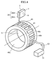
- the housing member 5 has a shape of a rectangular box with a space inside, and is installed circumferentially with respect to the ring-shaped unit-supporting section 40 (see Fig. 4) that is provided inside the casing 11A of the image acquisition device 11.
- the unit substrates 20 accommodated in the housing member 5 are arranged in 15 rows at required intervals so as not to overlap one another at progressively deeper positions (i.e., in the longitudinal direction of the bed 14).
- multiple coupling substrates 22 are arranged with required intervals at a rear end of the housing member 5 (i.e., on the right in Fig. 3B).
- Four substrate/circuit board fixing bars 32 extend in a longitudinal direction of the housing member 5 (i.e., in the longitudinal direction of the bed 14) to as to span between the inner walls of the housing member 5.
- the fixing bars 32 support the signal processor substrates 20B by extending through respective portions near four corners of each signal processor substrate 20B, so that the unit substrates 20 and the coupling substrates 22 are supported in the housing member 5.
- a unit fan 33 for air exhaust is provided at an upper section of the housing member 5.
- the unit fan 33 incorporate fans each rotationally driven by a thin-walled motor not shown, and has a function to discharge internal air of the housing member 5 towards an exhaust duct 43 (see Fig. 2) that is provided thereabove (externally thereto).
- the unit fan 33 operates on the electric power supplied from the low-voltage power supply (not shown) that is connected to the coupling substrate 22.
- the unit fan 33 may be of a normally actuated type or may be constructed so as to operate by detecting the fact that an internal temperature of the housing member 5 has reached a required value. Electric power consumption can be suppressed by constructing the unit fan in this way.
- the housing member 5 internally has an adiabatic member 7 that functions as a partitioning member to segment the member 5 into a first region A in which the detector 21 is disposed, and a second region B in which the signal processor.
- the adiabatic member 7 is provided in a sealed-up condition with a required thickness in various spatial clearances S1.
- the spatial clearances S1 are formed, as shown in Fig. 3B, between unit substrates 20, between one unit substrate 20 and one coupling substrate 22, between one unit substrate 20 and an inner side face 5b of the housing member 5, and between one coupling substrate 22 and the inner side face 5b of the housing member 5, at the connector C1 positions of the unit substrates 20, and as shown in Fig.
- the adiabatic member 7 exists to segment the inside of the housing member 5 into an inner spatial clearance thereof (the first region A) in which all detectors 21 of the detector substrate 20A are positioned, and another inner spatial clearance thereof (the second region B) in which the signal processor substrate 20B and the coupling substrate 22 are positioned.
- the existence of the adiabatic member 7 makes it possible to prevent internal heat of the integrated circuits (such as digital ASIC 26) in the second region B from being propagated to the first region A, and hence to prevent the detector 21 from being exposed to high temperature.
- a material, such as urethane, that is of low thermal conductivity and has an excellent filling-in property with respect to the spatial clearances S1 can be used as the adiabatic member 7.
- the member 7 is made of the urethane wrapped up in an electromagnetic wave shielding member capable of shielding electromagnetic waves, for example, a metallic sheet.
- an electromagnetic wave shielding member allows protection of the detector 21 from the electromagnetic waves originating from the integrated circuits such as the digital ASIC 26.
- the detector 21 can be enhanced in time resolution and in energy resolution.
- an adiabatic member 7 made from a resilient material, for example, rubber further simplifies the sealing-up of the spatial clearances S1.
- the unit substrate 20 vibrates during transport of the PET apparatus 1, the vibration can be appropriately suppressed.
- this position of the filler is only an example and the filler may be provided at any position in which the heat generated from the integrated circuits such as the digital ASIC 26 can be prevented from being transferred to the detector 21.
- the position of the filler in that case may be below and near the integrated circuits such as the digital ASIC 26.
- the coolant discharging element 6 is constructed of a unit fan 33 and a large number of ventilation holes 34.
- the unit fan 33 forcibly discharges the internal air of the housing member 5 to the outside thereof and is provided at a 180°-opposite position with respect to each detector 21, with each signal processor substrate 20B being positioned between the fan unit 33 and detector 21 in the housing member 5.
- the unit fan 33 is positioned at an upper section of the housing member 5 shown in Figs. 3A and 3B.
- Each ventilation hole 34 adapted to introduce cooling air from the outside of the detector unit 2 into the housing member 5 is formed in both inner side portions 5a of the member 5 in a lateral direction thereof (i.e., in a circumferential direction thereof in Fig. 2).
- each signal processor substrate 20B is introduced from a lateral direction with respect to a face of each signal processor substrate 20B.
- four ventilation holes 34 are formed in each side portion 5a, along the signal processor substrate 20B.
- the array of ventilation holes 34 shown in Fig. 3A is formed in multiple sets (e.g., as many as there actually are the signal processor substrates 20B and the coupling substrates 22) in a layout direction of the signal processor substrates 20B (i.e., in the longitudinal direction of the bed 14). This makes it possible to introduce an approximately uniform, desired amount of air into the housing member 5 and uniformly cool each signal processor substrate 20B and each coupling substrate 22.
- each ventilation hole 34 is formed at a position near the detectors 21 (the first region A), in other words, at the position most distant from the unit fans 33. This makes it possible, as indicated by dashed lines in Fig. 5, to circulate cooling air evenly through the signal processor substrate 20B and the coupling substrate 22 in their entirety, and to raise cooling efficiency.
- a ventilation port 8 is positioned at where it communicates with the first region A, in a longitudinal rear side portion 5d of the housing member 5.
- an anti-dust filter 9 is provided in such a form as to cover the entire ventilation port 8.
- the position of the ventilation port 8 having the anti-dust filter 9 is not limited to the longitudinal rear side portion 5d of the housing member 5 and may be in any other side portion thereof or at a lower portion 5e thereof.
- the ventilation port 8 with the anti-dust filter 9 may be provided in multiple places, not one place.
- the element that can be used as the anti-dust filter 9 examples include a HEPA (High-Efficiency Particulate Air) filter.
- the anti-dust filter 9 is not limited to a type constructed of a single filter, and may be a combination of multiple kinds of filters. Additionally, the anti-dust filter 9 does not always need to be a HEPA filter and may be any other kind of filter, such as a type formed from paper, an unwoven cloth, or the like. Ingress of dust and the like from the outside of the housing member 5 into the first region A where a large number of detectors 21 are provided can be prevented by providing such an anti-dust filter 9 at the ventilation port 8 in the housing member 5. Furthermore, if the ventilation port 8 with the anti-dust filter 9 is provided on a side not opposite to an adjacent detector unit 2, this allows each detector unit 2 to be arranged more densely and detection sensitivity to be improved.
- the detector unit 2 with the thus-constructed housing member 5 is installed in the unit-supporting section 40 set up inside the casing 11A (see Fig. 2) of the image acquisition device 11.
- the unit-supporting section 40 is ring-shaped and has multiple openings 40a at required intervals in a circumferential direction of the supporting section 40, on an outer peripheral surface thereof.
- the unit-supporting section 40 is constructed so that one detector unit 2 is inserted from the side of the detector substrate 20A of the unit substrate 20 into each opening 40a. Fixing the detector unit 2 to the unit-supporting section 40 is conducted using, for example, screws that are not shown.
- the detector unit 2 is constructed to be attachable and removable to and from the unit-supporting section 40, and maintenance and the like are facilitated.
- the housing members 5 of the adjacent detector units 2 are arranged close to one another at a very small angle, radiation detection sensitivity can be improved with a minimum quantity of ⁇ -rays passing there through. Inspection time can therefore be reduced.
- the cooler 50 mainly includes an air blower 51, a duct 52 for introducing air from the blower 51 into the unit-supporting section 40, an air guideway 42, an air exhaust duct 43 provided so as to encircle the outside of the air guideway 42, and air exhaust fans 44 provided on the exhaust duct 43.
- the air guideway 42 is, as shown in Fig. 5, defined between an opening verge 40b, the side portions 5a of the housing members 5, and a top plate 42a spanned between the adjacent housing members 5 and is formed between the adjacent housing members 5.
- the blower 51 and the duct 52 are installed outside the casing 11A.
- the blower 51 is disposed at a lateral or rear end (or the like) of the image acquisition device 11 or at any other location unobtrusive to, for example, operation or maintenance of the image acquisition device 11.
- the blower 51 uses a built-in fan to take in air from a room in which the image acquisition device 11 is installed, and supplies the air to the air guideway 42 through the duct 52 first and then a flow passageway not shown.
- An air-cleaning filter not shown is installed on an air intake side of the blower 51, and air that has passed through the air-cleaning filter is used as cooling air.
- This air-cleaning filter can be a HEPA filter of high dust-collecting performance, an electric type of dust-collecting filter, or the like.
- the air guideway 42 communicates with the second region B inside the housing member 5 via the ventilation hole 34 in the side portion 5a of the housing member 5.
- the exhaust duct 43 communicates with the inside of the housing member 5 via the unit fan 33, and the air inside the housing member 5 is discharged towards the exhaust duct 43 by the driving of the unit fan 33.
- the exhaust hole 43a opened in the installation room of the image acquisition device 11 is provided in a total of three places in the exhaust duct 43, and the air inside the exhaust duct 43 is discharged into the room through the exhaust fans 44 at the exhaust holes 43a.
- the present embodiment is constructed so that the air inside the installation room of the image acquisition device 11 is used as cooling air, and re-discharged into an examination room after cooling
- the present invention may be adapted to take in air from an exterior of the examination room and re-discharge the air therefrom after cooling.
- the blower 51, the unit fans 33 and the exhaust fan 44 operate synchronously with operation of the image acquisition device 11. Cooling air is sent from the blower 51 via the duct 52 to the air guideway 42 in the unit-supporting section 40, and the sent cooling air is introduced into the second region B of each housing member 5 through each ventilation hole 34 in the side portion 5a of the housing member 5. At this time, since the unit fans 33 are driven and the air in the second region B of the housing member 5 is forcibly discharged, the air in the second region B of the housing member 5 flows from the ventilation hole 34, towards the unit fan 33, as indicated by the dashed lines in Fig. 5. This flow of the air cools the integrated circuits such as the analog ASICs 24, thus allowing a temperature rise of the second region B to be suppressed.
- Cooling air that has been supplied to the inside of the housing member 5 is forcibly discharged into the exhaust duct 43.
- the after-cooling air, after being discharged from the exhaust duct 43, is re-discharged from the exhaust hole 43a into the room by the exhaust fan 44 provided at the exhaust hole 43a. In this way, the cooler 50 conducts cooling using cooling air.
- the cooler 50 On the air intake side connected to the unit-supporting section 40, the cooler 50 has a filter not shown, and this filter prevents dust of a relatively large particle size from being introduced into the image acquisition device 11.
- the filter is provided because an attempt to remove dust of a particle size smaller than necessary lowers an aperture ratio, resulting in a passage of air that is not smooth and thus results in reduced cooling capability. Accordingly, dust that is too small in particle size for the filter within the cooler 50 to remove will circulate through each detector unit 2. Consequently, the inside of the detector unit 2 will be laden with dust in the second region B during an extended time of operation.
- the housing member 5 is internally segmented into the first region A having the detectors 21 arranged therein, and the second region B accommodating the analog ASICs 24 (signal processors) and other integrated circuits.
- ASICs 24 signal processors
- Formation of very small clearances may therefore occur, for example, between the adiabatic member 7 and the unit substrate 20, between the adiabatic member 7 and the coupling substrate 22, between the adiabatic member 7 and the inner side faces 5b of the housing member 5, and between the adiabatic member 7 and internal corners of the housing member 5.
- deterioration of the adiabatic member 7 itself may form such minute clearances as mentioned above.
- the flow of air (upward air current) occurring in the second region B will cause the air in the second region B to be taken in via the above-mentioned clearances during the operation of the unit fan 33, and result in the inside of the second region B being filled with a negative pressure. If the unit fan 33 stops operating after that, the air in the second region B will immediately flow into the first region A. The flow of the air into the first region A, therefore, will also cause a simultaneous inflow of the dust that has accumulated in the second region B. This inflow of the dust will cause dust to stick to the detectors 21, hence resulting in a problem in that the detectors 21 characteristics would deteriorate.
- the entire examination room, with the PET apparatus 1 placed therein, is air-conditioned for low-humidity air to be incorporated into the detector units 2 during the operation of the PET apparatus 1. Therefore, if the present embodiment does not include the ventilation port 8 and the first region A is maintained in an incompletely enclosed condition by the presence of the foregoing minute clearances, humidity in the first region A with the detectors 21 provided therein will not immediately reach the value set by air-conditioning. The result would be that the humidity would become difficult to control. Even if humidity control is possible, a long time would be required for the humidity to reach its setting.
- providing the ventilation port 8 in the position where it communicates with the first region A of the housing member 5 makes it possible to prevent the first region A from being filled with a negative pressure. It is therefore possible to prevent the flow of air from the second region B via very small clearances into the first region A during the operational stop of the unit fan 33, and thus to prevent accumulated dust in the second region B from entering the first region A. Accordingly, it is possible to avoid the inconvenience of the radiation detectors 21 being degraded in performance.
- the ingress of dust from the above-mentioned ventilation port 8 can also be prevented since an anti-dust filter 9 is installed so as to cover the entire ventilation port 8.
- the installation of the anti-dust filter 9 makes the first region A enter a state equal to an essentially open state, and allows the first region A to be adjusted to the humidity set by air-conditioning. Hence, humidity control of the first region A becomes easy.
- the present embodiment uses semiconductor radiation detectors as the radiation detectors
- the present invention is not limited to the use of this detector type and for example, scintillators may be used instead.
- the signal processors in that case can each be constructed of a photomultiplier and a position arithmetic device or the like. In this case, dust-proofing and moisture-proofing effects can likewise be obtained if a ventilation hole with an anti-dust filter is provided in each housing member that shrouds one such scintillator.
- the housing member 5 and unit-supporting section 40 shown in Fig. 4 are both constructed of an optical-shielding material such as aluminum or aluminum alloy, and are adapted so that there are no clearances permitting entry of light, including fit-in sections between both the housing member 5 and the unit-supporting section 40.
- the light coming in from a direction of the space S can be reliably prevented from reaching the detectors 21, by disposing a cylindrical plate 40C such that an outer peripheral surface is positioned near a lower end of the housing member 5.
- optical shielding performance can be improved by constructing the cylindrical plate 40c from an aluminum alloy (or aluminum).
- the light coming in from the direction of the space S can likewise be shielded by adopting a construction in which the housing member 5 is shrouded with, for example, an optical shielding cover (not shown).
- the detectors 21 could be coated with an optical shielding material so as to form an optical shielding film.
- a cooler 50A is constituted by an introducing member 60 and a discharging member 70.
- the introducing member 60 is, as shown in Fig. 6, provided on a rear panel side of the PET apparatus 1 and assumes an annular form to cover an entire rear panel side of the unit-supporting section 40. Also, the introducing member 60 includes a ring-shaped inner pipe 61a, a ring-shaped outer pipe 61b, a shielding section 61c coupling the inner pipe 61a and the outer pipe 61b with each other, multiple air intake fans 62, and a filter 63.
- the inner pipe 61a and the outer pipe 61b are formed with the same required length in a longitudinal direction.
- the shielding section 61c is coupled with both the inner pipe 61a and the outer pipe 61b, at an intermediate position (see Fig. 7) in the longitudinal direction thereof.
- Each air intake fan 62 is provided circumferentially with respect to the shielding section 61c.
- the filter 63 for preventing ingress of the dust contained in the air coming in from the outside of the PET apparatus 1 is disposed so as to cover the entire ring-shaped region sandwiched between the inner pipe 61a and the outer pipe 61b, on the rear panel side of the PET apparatus 1.
- cooling air from which has been removed the large-grain-size dust taken in from the outside of the PET apparatus 1, is introduced into an introducing section 71a.
- providing the multiple air intake fans 62 in the layout direction of the detector units 2 makes it possible to supply a uniform amount of cooling air to each air guideway 42 and cool each detector unit 2 uniformly.
- the discharging member 70 includes a frame 71 that covers each detector unit 2, and multiple exhaust fans 72.
- the frame 71 assumes a shape in which it shrouds the outside of each detector unit 2 protruding from the above-mentioned unit-supporting section 40.
- a space is also formed that extends from the opening verge 40b (see Fig. 7) of the unit-supporting section 40 and functioning as a passageway for air to flow outward with respect to the unit fan 33 of the detector unit 2 (i.e., towards an upper section of Fig. 7).
- an introducing section 71a communicating with each air guideway 42 described above is formed on a rear panel side of the frame 71.
- the exhaust fans 72 are, as shown in Fig. 6, spaced from each other in the layout direction of the detector units 2, on an outer surface of the frame 71. Providing multiple exhaust fans 72 in this form makes it possible to efficiently discharge exhaust air from each detector unit 2 to the exterior of the PET apparatus 1.
- each detector unit 2 is segmented into the first region A where the detectors 21 are accommodated, and the second region B where the signal processors are accommodated
- the present invention is not limited thereto and the segmentation may be performed by inserting a sponge-like material between unit substrates 20, between one unit substrate 20 and one coupling substrate 22, between one unit substrate 20 and one housing member 5, and between one coupling substrate 22 and one housing member 5.
- the housing member itself may be formed integrally with both the first region A and the second region B, instead of the adiabatic member 7 or any other independent member being used. That makes it possible to reduce the number of components required.
- the present embodiment has been described taking the adiabatic member 7 as an example of the member for implementing the segmentation into the first region A and the second region B, the present invention is not limited to this example and using a conductive material, instead of the adiabatic member 7, allows the electromagnetic waves emitted from the signal processors to be stopped from propagating to the detectors 21.
Landscapes
- Health & Medical Sciences (AREA)
- Life Sciences & Earth Sciences (AREA)
- Engineering & Computer Science (AREA)
- Physics & Mathematics (AREA)
- High Energy & Nuclear Physics (AREA)
- Molecular Biology (AREA)
- Medical Informatics (AREA)
- Nuclear Medicine, Radiotherapy & Molecular Imaging (AREA)
- Biomedical Technology (AREA)
- Spectroscopy & Molecular Physics (AREA)
- General Physics & Mathematics (AREA)
- Optics & Photonics (AREA)
- Pathology (AREA)
- Radiology & Medical Imaging (AREA)
- Biophysics (AREA)
- Heart & Thoracic Surgery (AREA)
- Surgery (AREA)
- Animal Behavior & Ethology (AREA)
- General Health & Medical Sciences (AREA)
- Public Health (AREA)
- Veterinary Medicine (AREA)
- Nuclear Medicine (AREA)
- Measurement Of Radiation (AREA)
Applications Claiming Priority (1)
| Application Number | Priority Date | Filing Date | Title |
|---|---|---|---|
| JP2005289262A JP3942188B2 (ja) | 2005-09-30 | 2005-09-30 | 核医学診断装置、陽電子放出型断層撮影装置及び検出器ユニット |
Publications (1)
| Publication Number | Publication Date |
|---|---|
| EP1780557A2 true EP1780557A2 (fr) | 2007-05-02 |
Family
ID=37865964
Family Applications (1)
| Application Number | Title | Priority Date | Filing Date |
|---|---|---|---|
| EP06020152A Withdrawn EP1780557A2 (fr) | 2005-09-30 | 2006-09-26 | Appareil de diagnostic en médecine nucléaire, appareil de tomographie à émission de positrons et unités de détection |
Country Status (4)
| Country | Link |
|---|---|
| US (1) | US7511277B2 (fr) |
| EP (1) | EP1780557A2 (fr) |
| JP (1) | JP3942188B2 (fr) |
| CN (1) | CN1940596A (fr) |
Cited By (1)
| Publication number | Priority date | Publication date | Assignee | Title |
|---|---|---|---|---|
| US20160006952A1 (en) * | 2013-03-22 | 2016-01-07 | Mitsubishi Heavy Industries, Ltd. | Camera |
Families Citing this family (39)
| Publication number | Priority date | Publication date | Assignee | Title |
|---|---|---|---|---|
| JP4365762B2 (ja) * | 2004-09-30 | 2009-11-18 | 株式会社日立製作所 | 核医学診断装置および核医学診断装置の冷却方法 |
| US7488943B2 (en) * | 2006-07-17 | 2009-02-10 | General Electric Company | PET detector methods and apparatus |
| DE102007009180B4 (de) * | 2007-02-26 | 2017-05-18 | Siemens Healthcare Gmbh | Kombinationstomograph |
| JP5042757B2 (ja) * | 2007-09-21 | 2012-10-03 | 富士フイルム株式会社 | 放射線画像撮影装置 |
| DE102008036289B4 (de) * | 2008-08-04 | 2012-01-12 | Siemens Aktiengesellschaft | Kombiniertes MR-PET-Gerät |
| JP5197265B2 (ja) * | 2008-09-22 | 2013-05-15 | 富士フイルム株式会社 | 放射線撮影装置 |
| KR101269782B1 (ko) | 2008-10-03 | 2013-05-30 | 도시바 덴시칸 디바이스 가부시키가이샤 | 방사선 검출 장치와 방사선 촬영 장치 |
| JP2010099396A (ja) * | 2008-10-27 | 2010-05-06 | Toshiba Corp | Pet−ct装置 |
| US8378306B2 (en) * | 2010-07-21 | 2013-02-19 | Siemens Medical Solutions Usa, Inc. | Dual amplifier for MR-PET hybrid imaging system |
| BR112014015757A8 (pt) | 2011-12-27 | 2017-07-04 | Koninklijke Philips Nv | quadro; módulo de detecção de radiação; digitalizador de pet; e método de montar uma matriz de detectores de radiação |
| US10987069B2 (en) | 2012-05-08 | 2021-04-27 | Spectrum Dynamics Medical Limited | Nuclear medicine tomography systems, detectors and methods |
| JP6049166B2 (ja) * | 2012-05-16 | 2016-12-21 | 株式会社日立製作所 | 半導体放射線検出器およびそれを用いた核医学診断装置 |
| CN103860187B (zh) * | 2012-12-10 | 2015-05-13 | 上海联影医疗科技有限公司 | 一种正电子发射断层扫描仪的冷却系统 |
| DE102013203894B4 (de) * | 2013-03-07 | 2017-07-27 | Siemens Healthcare Gmbh | Röntgendetektor, Röntgensystem und Verfahren zur Messung des Partikelzustands des Röntgendetektors |
| JP2014210047A (ja) * | 2013-04-18 | 2014-11-13 | 株式会社東芝 | X線ct装置 |
| CN104382609B (zh) * | 2014-10-28 | 2017-02-01 | 沈阳东软医疗系统有限公司 | 一种准直器、扫描设备及其使用方法 |
| US10375901B2 (en) | 2014-12-09 | 2019-08-13 | Mtd Products Inc | Blower/vacuum |
| US9709686B2 (en) * | 2014-12-30 | 2017-07-18 | General Electric Company | Modular positron emission tomography (PET) gantry |
| US10314551B2 (en) * | 2015-06-16 | 2019-06-11 | The Trustees Of Princeton University | Detector, three-dimensional direct positron imaging unit, and method to estimate the differential of the radiation dose provided to cancer cells and healthy tissues during hadrotherapy |
| US10663608B2 (en) | 2015-09-21 | 2020-05-26 | Shanghai United Imaging Healthcare Co., Ltd. | System and method for calibrating a PET scanner |
| KR102405926B1 (ko) * | 2015-11-12 | 2022-06-07 | 프리스매틱 센서즈 에이비 | 시간 오프셋된 심도 구획부를 구비한 에지-온 검출기를 사용하는 고해상도 전산화 단층촬영(high-resolution computed tomography using edge-on detectors with temporally offset depth-segments) |
| WO2017101620A1 (fr) * | 2015-12-18 | 2017-06-22 | Shanghai United Imaging Healthcare Co., Ltd. | Système et procédé de refroidissement de système d'imagerie |
| CN105704982B (zh) | 2015-12-18 | 2017-12-22 | 上海联影医疗科技有限公司 | 一种用于医学成像装置的冷却系统 |
| KR101785206B1 (ko) * | 2016-05-30 | 2017-10-17 | 고려대학교 산학협력단 | 극저온 양전자 방출 단층 촬영장치 |
| US10054698B2 (en) | 2016-08-31 | 2018-08-21 | General Electric Company | Temperature stabilization for detector heads |
| JP2018079032A (ja) * | 2016-11-15 | 2018-05-24 | 富士フイルム株式会社 | 放射線画像撮影装置及び熱拡散方法 |
| EP3698326A4 (fr) | 2017-10-19 | 2021-08-11 | Spectrum Dynamics Medical Limited | Étalonnage et contrôle qualité d'un système d'imagerie radio de médecine nucléaire (n-m) |
| US11903749B2 (en) * | 2017-10-19 | 2024-02-20 | Spectrum Dynamics Medical Limited | Nuclear medicine tomography system comprising a detector carrier housing and a heat pump configured to cool air within the detector carrier housing |
| CN108392218B (zh) * | 2018-04-13 | 2024-03-29 | 湖北锐世数字医学影像科技有限公司 | 一种pet设备的风冷装置 |
| CN109100776B (zh) * | 2018-08-28 | 2022-11-08 | 上海联影医疗科技股份有限公司 | 一种探测器组件及探测器系统 |
| CN110448325B (zh) * | 2019-09-02 | 2024-09-06 | 明峰医疗系统股份有限公司 | 一种pet系统风冷散热装置 |
| CN111190216B (zh) * | 2020-01-23 | 2023-03-24 | 中国工程物理研究院激光聚变研究中心 | 一种辐射流探测器阵列 |
| CN111557680A (zh) * | 2020-06-01 | 2020-08-21 | 南京安科医疗科技有限公司 | 一种用于头部ct系统的ct探测器 |
| KR20230109134A (ko) * | 2020-11-25 | 2023-07-19 | 하마마츠 포토닉스 가부시키가이샤 | 촬상 유닛 및 촬상 시스템 |
| CN113038758B (zh) * | 2021-03-17 | 2022-09-30 | 明峰医疗系统股份有限公司 | 一种风冷散热装置及应用该装置的风冷系统 |
| US20250044465A1 (en) * | 2023-08-04 | 2025-02-06 | Canon Kabushiki Kaisha | Radiation detection apparatus, manufacturing method thereof, and system |
| CN222604579U (zh) * | 2024-04-29 | 2025-03-14 | 上海联影医疗科技股份有限公司 | 探测器散热装置及其探测器组件 |
| KR102855066B1 (ko) * | 2024-09-27 | 2025-09-09 | (주)에프티글로벌 | 냉각시스템이 구비된 양전자 방출 단층 촬영 장치 |
| CN119523507A (zh) * | 2024-10-31 | 2025-02-28 | 纳米维景(上海)医疗科技有限公司 | 一种降噪温控的静态ct设备及系统 |
Family Cites Families (8)
| Publication number | Priority date | Publication date | Assignee | Title |
|---|---|---|---|---|
| JP3856511B2 (ja) | 1996-11-29 | 2006-12-13 | 株式会社日立メディコ | ポジトロンct装置用ガントリ |
| JP2001245878A (ja) | 2000-03-02 | 2001-09-11 | Hitachi Medical Corp | X線ct装置 |
| US6586744B1 (en) * | 2000-11-24 | 2003-07-01 | Marconi Medical Systems, Inc. | Method of cooling high density electronics |
| JP2003194951A (ja) | 2001-12-28 | 2003-07-09 | Canon Inc | X線撮影装置 |
| DE10304661B4 (de) * | 2003-02-05 | 2007-03-01 | Siemens Ag | Kühlsystem und Verfahren zur Kühlung einer Gantry |
| JP2005128000A (ja) | 2003-09-30 | 2005-05-19 | Hitachi Ltd | 核医学診断装置 |
| US7065173B2 (en) * | 2003-12-02 | 2006-06-20 | General Electric Company | Method and apparatus for thermal management of CT electronics |
| JP4303603B2 (ja) * | 2004-01-13 | 2009-07-29 | 株式会社日立製作所 | 核医学診断装置、及びその検出器ユニット |
-
2005
- 2005-09-30 JP JP2005289262A patent/JP3942188B2/ja not_active Expired - Fee Related
-
2006
- 2006-09-22 US US11/524,919 patent/US7511277B2/en not_active Expired - Fee Related
- 2006-09-22 CN CN200610139302.2A patent/CN1940596A/zh active Pending
- 2006-09-26 EP EP06020152A patent/EP1780557A2/fr not_active Withdrawn
Cited By (3)
| Publication number | Priority date | Publication date | Assignee | Title |
|---|---|---|---|---|
| US20160006952A1 (en) * | 2013-03-22 | 2016-01-07 | Mitsubishi Heavy Industries, Ltd. | Camera |
| EP2950120A4 (fr) * | 2013-03-22 | 2016-03-16 | Mitsubishi Heavy Ind Ltd | Caméra |
| US10070073B2 (en) | 2013-03-22 | 2018-09-04 | Mitsubishi Heavy Industries, Ltd. | Camera for visualizing states of distribution of radioactive substances |
Also Published As
| Publication number | Publication date |
|---|---|
| US20070080296A1 (en) | 2007-04-12 |
| US7511277B2 (en) | 2009-03-31 |
| JP3942188B2 (ja) | 2007-07-11 |
| CN1940596A (zh) | 2007-04-04 |
| JP2007101273A (ja) | 2007-04-19 |
Similar Documents
| Publication | Publication Date | Title |
|---|---|---|
| US7511277B2 (en) | Nuclear medicine diagnostic apparatus, positron emission computed tomography apparatus, and detector units | |
| JP4365762B2 (ja) | 核医学診断装置および核医学診断装置の冷却方法 | |
| US7342234B2 (en) | Radiological imaging apparatus and cooling method of same | |
| US20080103391A1 (en) | Tomography by Emission of Positrons (Pet) System | |
| CN113287056B (zh) | 基于准直器和检测器的医学成像系统 | |
| JP5126049B2 (ja) | 核医学診断装置、形態断層撮影診断装置、核医学用データ演算処理方法および形態断層画像演算処理方法 | |
| KR20090073040A (ko) | 핵의학 진단장치, 형태단층촬영 진단장치, 핵의학용 데이터연산처리방법 및 형태단층화상 연산처리방법 | |
| US9658086B1 (en) | Reduced airborne contamination detector heads | |
| US6472668B1 (en) | High voltage distribution system for CZT arrays | |
| JP2005201671A (ja) | 核医学診断装置、及びその検出器ユニット | |
| JP2008164548A (ja) | 放射線撮像装置 | |
| JP4429723B2 (ja) | 高密度電子装置の冷却方法 | |
| JP2007101234A (ja) | 核医学診断装置および核医学診断装置の冷却方法 | |
| Sánchez-Crespo et al. | The influence of photon depth of interaction and non-collinear spread of annihilation photons on PET image spatial resolution | |
| JP2007101556A (ja) | 核医学診断装置、陽電子放出型断層撮影装置及び検出器ユニット | |
| US9689720B1 (en) | Reduced airborne contamination detector heads | |
| JP3604491B2 (ja) | ガンマカメラ装置 | |
| JP2006284346A (ja) | 放射線断層撮影装置 | |
| CN110383107A (zh) | 减少空气传播污染的检测器头部 | |
| JP4082324B2 (ja) | 陽電子放出型ct装置 | |
| US9348033B2 (en) | Positron CT apparatus | |
| US7554088B2 (en) | Method for positron emission imaging | |
| JP2004061122A (ja) | Cztアレイのための高電圧配電システム | |
| Reilly | Nuclear Medicine Imaging Technology | |
| Elliott | Practical instrumentation |
Legal Events
| Date | Code | Title | Description |
|---|---|---|---|
| PUAI | Public reference made under article 153(3) epc to a published international application that has entered the european phase |
Free format text: ORIGINAL CODE: 0009012 |
|
| AK | Designated contracting states |
Kind code of ref document: A2 Designated state(s): AT BE BG CH CY CZ DE DK EE ES FI FR GB GR HU IE IS IT LI LT LU LV MC NL PL PT RO SE SI SK TR |
|
| AX | Request for extension of the european patent |
Extension state: AL BA HR MK YU |
|
| STAA | Information on the status of an ep patent application or granted ep patent |
Free format text: STATUS: THE APPLICATION HAS BEEN WITHDRAWN |
|
| 18W | Application withdrawn |
Effective date: 20070831 |