EP1780559B1 - Capteur optique - Google Patents
Capteur optique Download PDFInfo
- Publication number
- EP1780559B1 EP1780559B1 EP20060022107 EP06022107A EP1780559B1 EP 1780559 B1 EP1780559 B1 EP 1780559B1 EP 20060022107 EP20060022107 EP 20060022107 EP 06022107 A EP06022107 A EP 06022107A EP 1780559 B1 EP1780559 B1 EP 1780559B1
- Authority
- EP
- European Patent Office
- Prior art keywords
- optoelectronic device
- mirror
- light beams
- transmitted light
- receiver
- Prior art date
- Legal status (The legal status is an assumption and is not a legal conclusion. Google has not performed a legal analysis and makes no representation as to the accuracy of the status listed.)
- Ceased
Links
- 230000003287 optical effect Effects 0.000 title 1
- 230000005693 optoelectronics Effects 0.000 claims description 86
- 238000012544 monitoring process Methods 0.000 claims description 15
- 230000004888 barrier function Effects 0.000 claims description 11
- 238000001514 detection method Methods 0.000 claims description 10
- 238000011156 evaluation Methods 0.000 claims description 9
- 238000010586 diagram Methods 0.000 description 5
- 125000006850 spacer group Chemical group 0.000 description 4
- 230000008901 benefit Effects 0.000 description 2
- 230000008859 change Effects 0.000 description 2
- 238000011161 development Methods 0.000 description 2
- 230000018109 developmental process Effects 0.000 description 2
- 230000000737 periodic effect Effects 0.000 description 2
- 230000011514 reflex Effects 0.000 description 2
- 230000008719 thickening Effects 0.000 description 2
- 244000089486 Phragmites australis subsp australis Species 0.000 description 1
- 229920005372 Plexiglas® Polymers 0.000 description 1
- 230000002238 attenuated effect Effects 0.000 description 1
- 230000005540 biological transmission Effects 0.000 description 1
- 230000015572 biosynthetic process Effects 0.000 description 1
- 238000010276 construction Methods 0.000 description 1
- 238000011109 contamination Methods 0.000 description 1
- 238000013016 damping Methods 0.000 description 1
- 230000000694 effects Effects 0.000 description 1
- 238000005259 measurement Methods 0.000 description 1
- 239000004926 polymethyl methacrylate Substances 0.000 description 1
- 230000005855 radiation Effects 0.000 description 1
- 230000004044 response Effects 0.000 description 1
- 238000007493 shaping process Methods 0.000 description 1
- 238000012549 training Methods 0.000 description 1
- 230000007704 transition Effects 0.000 description 1
- 230000001960 triggered effect Effects 0.000 description 1
Images




Classifications
-
- G—PHYSICS
- G01—MEASURING; TESTING
- G01V—GEOPHYSICS; GRAVITATIONAL MEASUREMENTS; DETECTING MASSES OR OBJECTS; TAGS
- G01V8/00—Prospecting or detecting by optical means
- G01V8/10—Detecting, e.g. by using light barriers
- G01V8/12—Detecting, e.g. by using light barriers using one transmitter and one receiver
- G01V8/14—Detecting, e.g. by using light barriers using one transmitter and one receiver using reflectors
Definitions
- the invention relates to an optoelectronic device.
- An optoelectronic device of the type in question is known from DE 101 35 036 A1 known.
- the optoelectronic device described therein forms a frame light barrier with a laser diode for generating a light beam at a periodic reflection angle and first and second opposing planar mirror surfaces.
- the scanner mirror and the first and second mirror surfaces are arranged such that a generated light beam is reflected back and forth by the scanner mirror onto the first mirror surface, from there to the second mirror surface, between the first and second mirror surfaces, and then onto the light receiver.
- a device for generating a light band comprising a laser diode for generating a light beam, a scanner mirror for reflecting the light beam at a periodic reflection angle and a deflection prism for generating a substantially uniform light band on a CCD line.
- a disadvantage of this optoelectronic device is their high susceptibility to interference. This is based on the fact that the flat mirror surfaces must be aligned extremely exactly parallel to each other, so that the light rays can be guided in a desired manner along these mirror surfaces. However, even the smallest recesses of these mirror surfaces lead to a lateral escape of the light rays, so that it is no longer functional.
- a device is known from EP A 0 021 163 known.
- This device forms an anti-burglary protection for surfaces in which the edge of the surface to be protected is provided with light-reflecting layers which direct the light emanating from a light source to a receiver and in which alarm is triggered upon influencing this light.
- the light-reflecting layers are formed of elements which reflect an incident light beam independently of its angular position in the plane defined by the layers parallel to its direction of incidence. These elements are designed as mirror strips containing 90 ° angle mirrors or 90 ° orbits as reflective elements. Several such mirrors or prisms can be grouped together in a mirror bar.
- the DE 195 33 044 A1 relates to a double light barrier.
- This light barrier consists of a transmitter / receiver part and a reflector part, wherein the transmitter and the receiver are facing away from one another in a plane and the reflector part has reflective elements such that a light beam emitted by the transmitter is mirrored so that a back-plate is formed runs parallel to the emitted light beam and hits the receiver.
- the reflector part to the light barrier has an array of reflective elements such that the distance between the transmitter and the receiver is bridged and form a triple mirror, through which the received first barrier beam is reflected at a corresponding distance as a second, parallel barrier beam. If one or the other barrier beam is interrupted, the light barrier emits a switching signal.
- the DE 195 04 230 A1 relates to an optoelectronic device having a transmission element emitting a transmitting light beam and a receiving element remote from the transmitting element, on which the transmitted light beam is guided via at least one deflection unit.
- the transmitted light rays is in a level led.
- the deflecting unit has two mirror-symmetrically arranged, perpendicular to the plane, flat mirror surfaces which are arranged opposite one another at a fixed predetermined angle so that the transmitted light beam is reflected once at the mirror surfaces.
- the deflection unit is rotatable about an axis of rotation perpendicular to the plane of the transmitted light beam.
- the invention has the object of providing an optoelectronic device of the type mentioned in such a way that it has the lowest possible susceptibility to interference with high functionality.
- the optoelectronic device is used to detect objects in a surveillance area and consists of a transmit light emitting emitter, a receiving light beam receiving receiver, an evaluation unit for generating an object detection signal in response to the received signals of the receiver and two monitoring areas delimiting mirror parts.
- the transmitted light rays are guided by reflections on these mirror parts of the transmitter and receiver.
- At least one of the mirror parts has at least two mutually inclined mirror surfaces on which the transmitted light beams are deflected transversely to the direction of propagation.
- the transmitter and receiver form a distance sensor element by means of which the transit time of the transmitted light beams is determined by the monitoring area. To check the function of the optoelectronic device, the determined transit time of the transmitted light beams is compared by the monitoring area with a desired value.
- the optoelectronic device Since the transmitter and the receiver, a distance sensor, by means of which the duration of the transmitted light beams is controlled, the reliability of the optoelectronic device increases. Thus, the optoelectronic device according to the invention is also suitable for safety applications.
- a significant advantage of the invention is that stabilized by the formation of at least one of the mirror parts with mutually inclined mirror surfaces by the conditional beam guidance of the transmitted light beams transversely to the propagation direction such that the optoelectronic device is insensitive to lateral tilting of the mirror parts.
- the mirror parts of the optoelectronic device therefore do not need to be adjusted exactly transversely to the direction of propagation, which considerably facilitates the fixing and mounting of the optoelectronic device. Since the functionality of the optoelectronic device still remains intact even with lateral tilting of the mirror parts, this has a low susceptibility to interference.
- a threshold value evaluation of the received signals of the receiver preferably takes place.
- the resulting switching signal indicates whether an object is in the surveillance area or not.
- the optoelectronic device By configuring the optoelectronic device with two opposing mirror parts extending along the surveillance area, the optoelectronic device can be formed as a light grid.
- the sensor components of the optoelectronic device can also form a concentric arrangement, which is particularly suitable for the detection of small parts in pipes.
- FIG. 1 shows the block diagram of an optoelectronic device 1 with a transmitter 2, which emits transmitted light beams 3 in a region to be monitored. Furthermore, the optoelectronic device 1 comprises a receiving light beams 4 receiving receiver 5.
- the transmitter 2 is formed by a light emitting diode.
- the receiver 5 may be formed as a photodiode.
- the transmitted light beams 3 are guided between two mirror parts 7, 7 'and then guided as receiving light beams 4 to the receiver 5.
- a sensor-side mirror part 7 and a distance to this further mirror part 7 ' is provided. Due to the multiple reflection of the transmitted light beams 3 between the two mirror parts 7 and 7 ', the object 6 is reliably detected even in small dimensions in the surveillance area.
- the transmitted light beams 3 are strongly attenuated and the film is reliably detected.
- the object detection takes place in such a way that a binary switching signal is derived from the received signals present at the receiver as an object detection signal, the switching states of which indicate whether or not an object is located in the monitored area.
- the switching signal is measured by a threshold value evaluation of the received signals at the output of the receiver 5.
- the evaluation takes place in an evaluation unit 8, which is accommodated with the other components of the optoelectronic device 1 in a housing 9.
- the switching signal is output via a switching output 10, which is connected to the Evaluation unit 8 is connected.
- a parameterization interface 11 is connected to the evaluation unit 8.
- FIG. 2 shows a variant of the optoelectronic device 1 according to FIG. 1 , which operates on the principle of the light barrier, wherein the mirror part 7 between the transmitter 2 and receiver 5 is arranged.
- the mirror parts 7, 7 ' are mounted in oppositely disposed parts of the housing 9.
- a transmitting optics 19 for beam shaping of the transmitted light beams 3 and a receiving optics 20 for focusing the received light beams 4 are provided on the receiver 5. Furthermore, in this part of the housing 15, a printed circuit board 21 is integrated, on which the transmitter 2 and receiver 5 and the components of the evaluation unit 8 not shown separately are arranged.
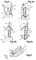
- FIG. 3 shows mirror parts 7, 7 'according to the prior art, each having flat mirror surfaces to guide the transmitted light beams 3 from the transmitter 2 via the mirror parts 7, 7' from the receiver 5. Even the slightest deviations from the parallel beam guidance lead as in FIG. 3 shown to a lateral escape of the received light beams 4, that is, these no longer reach the receiver.
- FIG. 4a shows a first embodiment of the mirror parts 7, 7 'according to the invention with surface mirrors, which are formed from two mirrors each, which are inclined by 90 ° to each other. As a result, a lateral escape of the received light beam 4 is prevented. It shows FIG. 4 the mirror parts 7, 7 'of an optoelectronic device 1 according to FIG FIG. 1 or 2 in cross section.
- FIG. 4b shows a cross-sectional view of a second embodiment of the mirror parts 7, 7 'of the optoelectronic device 1 according to FIG. 1 or 2 , wherein the sensor-side mirror part 7 is formed by a roof prism, whereby the false angle of the incident transmitted light beams 3 is not increased by the further reflections.
- the mirror part 7 ' has a flat mirror surface, which is formed by a plane mirror.
- Figure 4c shows a third embodiment, wherein both mirror parts 7, 7 'are formed by roof prisms.
- FIG. 5 shows a fourth embodiment, in which the mirror parts 7, 7 'are formed by roof prism panels.
- the advantage here is that the mirror parts 7, 7 'can be very flat.
- the propagation direction of the transmitted light beams 3 is in the X direction.
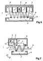
- FIG. 6 shows an extension of in FIG. 2 illustrated optoelectronic device 1 with an additional reference channel, which is not affected by an object 6.
- the reference channel is used to determine the basic attenuation of the free path, that is, the attenuation of the transmitted light beams 3 when passing through the object-free monitoring area.
- the reference channel is formed by a transmitter 2 'which emits transmitted light beams 3'.
- the transmitted light beams 3 'of the transmitter 2' are guided to the same receiver 5 as the transmitted light beams 3 of the transmitter 2, the transmitters 2, 2 'being activated alternately, so that the signals generated by the transmitters 2, 2' at the receiver 5 can be evaluated separately.
- Drift effects such as slow pollution or temperature-induced changes in angle can be compensated.
- FIG. 7 shows an embodiment of an optoelectronic device 1, which operates on the reflex and Autokollimationskal.
- the emitted light beams 3 emitted by the transmitter 2 are guided again via the mirror parts 7, 7 'within the surveillance area.
- the transmitter 2 and the receiver 5 are arranged side by side on the same side of the surveillance area. After the emitted light beams 3 emitted by the transmitter 2 are guided through the surveillance area for the first time, they meet a triple reflector 18.
- the triple light reflector 18 deflects the transmitted light beams 3 as received light beams 4.
- the received light beams 4 are like the transmitted light beams 3 passed through a common transmitting-receiving lens 17 and directed by a beam splitter 12 and a deflecting mirror 13 to the receiver 5.
- reflection light barriers can be used with polarizing filters, so that only received light beams 4 are taken into account by the triple reflector 18 and direct reflections from a mirror part 7, 7 'are suppressed.
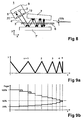
- FIG. 8 shows an embodiment of an optoelectronic device 1, in which the transmitter 2 and receiver 5 are arranged in a common housing 9.
- the transmitter 2 is assigned a transmitting optics 19
- the receiver 5 is associated with a receiving optics 20.
- the angle of incidence becomes the transmitted light beams 3 after each reflection larger.
- the transmitted light beams 3 reverse and reach the sensor as receiving light beams 4 in parallel with the transmitted light beams 3.
- FIG. 9b shows the diagram of the attenuation curve of the transmitted light beams 3 of the optoelectronic device 1 according to FIG. 8 at free range.
- the attenuation at entry and exit from the roof prism is each about 4%. If the mirror part 7 'formed by a surface plan mirror, can be expected with about 5% damping.
- Previous film sensors according to the reflection principle achieve only an attenuation to 84%, that is, taking into account tolerances, disturbances and contamination of about 10%, only about 6% remain as a functional reserve, resulting in a limited detection reliability.
- FIG. 10a - c show a variant of the optoelectronic device 1 according to FIG. 8 ,
- the optoelectronic device 1 shown in a longitudinal section differs from the optoelectronic device 1 according to FIG. 8 only with regard to the training of their mirror parts 7, 7 ', in FIG. 10b are shown in a plan view.
- the mirror parts 7, 7 'in the propagation direction of the transmitted light beams 3 is not inclined, yet with the mirror parts 7, 7' of the optoelectronic device 1 according to FIG. 10a-c a beam reversal of the transmitted light beams 3 is achieved.
- FIG. 10a a beam reversal by prismatic thickening at the beginning (area a), or tapering at the end (area c) of the mirror part 7 is reached.
- the region a ensures that the angle of incidence of the transmitted light beams 3 is reduced so that the transmitted light beams 3 are so dense in the region b that small parts are reliably detected, or clear films produce sufficient overall attenuation.
- the region c ensures that for the transmitted light beams 3, even with tolerances with respect to the alignment of the mirror parts 7, 7 'to each other, a beam reversal takes place, that is to say that the transmitted light beams 3 reverse in this area and then run as receiving light beams 4 back to the receiver 5.
- FIG. 10b shows the mirror parts 7, 7 'from the front, wherein the mirror part 7' can also be formed by a plane mirror. As can be seen from this illustration, both mirror parts 7, 7 'have a prism structure transversely to the propagation direction of the transmitted light beams 3.
- the distance d3 between the mirror parts 7, 7 'and the length of the regions a and c, the beam path of the transmitted light beams 3 and received light beams 5 is defined.
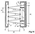
- FIG. 11 shows an embodiment of an optoelectronic device 1, which in terms of its construction of the optoelectronic device 1 according to FIG. 2 equivalent.
- the optoelectronic device 1 according to FIG. 11 differs according to the optoelectronic device 1 according to FIG. 2 only in terms of how it works.
- the optoelectronic device 1 according to FIG. 11 forms a safety light grid.
- the transmitter 2 and the receiver 5 form a distance sensor which operates according to the light transit time principle. This distance sensor is used to monitor the total radiation of the transmitted light beams 3 via the mirror parts 7, 7 'to the receiver 5, the transmitted light beams 3 in turn being reflected several times between the mirror parts 7, 7'.
- D2 is the distance between the transmitter 2 and the receiver 5.
- the distance d1 is as shown FIG. 11 can be seen from the difference in the location of incidence of the transmitted light rays 3 on the mirror part 7 'in the first two reflections of the transmitted light rays 3 formed on this mirror part 7'.
- the manipulation safety of the safety light grid is ensured by the distance measurement.
- the mirror parts 7, 7 'of the optoelectronic device 1 according to FIG. 11 have analogous to the embodiment according to FIG. 2 mutually inclined mirror surfaces according to the embodiments according to FIG. 4 on. If the mirror parts 7, 7 'would each have planar mirrors as mirror surfaces, would have to In the above example, the mirrors are aligned with each other to +/- 0.02 °, which would be impractical in the application.
- FIGS. 12a, b show an embodiment of an optoelectronic device 1, which serves to detect objects designed as small parts in a transparent tube 14.
- the hollow cylindrical tube 14 is made of Plexiglas, for example.
- the optoelectronic device 1 comprises a transmitting light rays 3 emitting transmitter 2 and a receiving light beams 4 receiving receiver 5. Furthermore, a larger mirror part 7 and two smaller mirror parts 7 'are provided. These are arranged in the circumferential direction of the tube 14 outside the tube 14, so that emitted by the transmitter 2 transmitted light beams 3 first meet the mirror part 7, are guided from there to the mirror parts 7 'and then impinge on the receiver 5 as receiving light beams 4. In this case, the transmitted light rays 3 pass through the tube 14 several times in a horizontal plane.
- the mirror parts 7, 7 ' are analogous to the embodiment according to FIG. 5 the form of roof prismatic panels through these prismatic structures, in turn, a lateral escape of the transmitted light beams 3 is prevented. Thus, the optoelectronic device 1 is insensitive to tilting of the mirror parts 7, 7 '.
- the transmitted light rays 3 extend in the radial direction through the transparent tube 14, so that defocusing is avoided by the curved wall of the tube 14.
- the minimum size d5 of the object 6 is determined by the number of mirror parts 7, 7 ', which can be increased if necessary.
- FIGS. 13a-d show a development of the optoelectronic device 1 according to the FIGS. 12a , b.
- the sensor components of the optoelectronic device 1, which correspond to the embodiment according to FIGS. 12a, b correspond are integrated in a housing 15.
- the housing 15 is formed as a hollow cylinder.
- the diameter of the housing 15 is dimensioned so that the tube 14 can be placed in the interior thereof, wherein also on the inner wall of the housing 15, the sensor components are mounted.
- FIG. 13a the housing 15 is subdivided into two housing segments 15 ', 15 "in order to be able to insert the tube 14 therein for mounting purposes.
- the spacers 16 ensure that the tube 14 is held in the center of the housing 15.
- FIG. 13b shows the spacers 16, which are formed of individual spring elements to evenly press and compensate for dimensional tolerances.
- FIG. 13c shows the spacer 16, when used on a pipe 14 of larger diameter. For this purpose, 16 so many spring elements are broken out of the spacer until the tube 14 is just pressed sufficiently again.
- FIG. 13d shows the multi-beam arrangement after FIG. 13a with the pipe diameter FIG. 13c , The housing half 15 "is removed to show how the pipe 14 can be inserted.
- FIG. 14 shows a variant according to FIG. 12 ,
- the optoelectronic device 1 according to FIG. 14 only two mirror parts 7 ', that is, no mirror part 7 is provided. Otherwise corresponds to the optoelectronic device according to FIG. 14 the embodiment according to FIG. 12 , Due to the reduced number of mirror parts 7 ', the transmitted light beams 3 are guided through the tube 14 only twice.
- FIG. 15 shows a further variant of the optoelectronic device 1 according to FIG. 12 ,
- this optoelectronic device 1
- four pairs of mirror parts 7, 7 ' are provided in addition to a transmitter 2 and a receiver 5, which are each formed identically.
- These sensor components are in turn arranged in the circumferential direction around the tube 14.
- the transmitted light beams 3 are each guided by a mirror part 7 to a mirror part 7 '.
- the transmitted light beams 3 are passed through the tube 14 five times.
Landscapes
- Physics & Mathematics (AREA)
- Life Sciences & Earth Sciences (AREA)
- General Life Sciences & Earth Sciences (AREA)
- General Physics & Mathematics (AREA)
- Geophysics (AREA)
- Geophysics And Detection Of Objects (AREA)
Claims (18)
- Dispositif optoélectronique pour détecter des objets dans une zone de surveillance, avec un émetteur (2) émettant des rayons lumineux d'émission (3), un récepteur (5) recevant des rayons lumineux de réception (4), une unité d'évaluation (8) pour générer un signal de détection d'objet en fonction des signaux de réception du récepteur (5), et avec deux parties réfléchissantes (7, 7') qui limitent la zone de surveillance, les rayons lumineux d'émission (3) étant guidés de l'émetteur (2) vers le récepteur (5) par des réflexions sur ces parties réfléchissantes (7, 7'), et au moins une des parties réfléchissantes (7) présentant au moins deux surfaces réfléchissantes inclinées l'une par rapport à l'autre, sur lesquelles les rayons lumineux d'émission (3) sont déviés transversalement à la direction de propagation, caractérisé en ce que l'émetteur (2) et le récepteur (5) forment un élément de capteur de distance au moyen duquel le temps de parcours des rayons lumineux d'émission (3) à travers la zone de surveillance est déterminé, le temps de parcours déterminé des rayons lumineux d'émission (3) à travers la zone de surveillance étant comparé avec une valeur de consigne pour contrôler le fonctionnement du dispositif optoélectronique.
- Dispositif optoélectronique selon la revendication 1, caractérisé en ce que l'atténuation des rayons lumineux d'émission (3) se produisant lors d'une entrée d'un objet dans la zone de surveillance est enregistrée pour générer une signalisation d'objet.
- Dispositif optoélectronique selon la revendication 2, caractérisé en ce que le signal de détection d'objet est conçu comme un signal de commutation binaire qui est obtenu par une évaluation de valeur seuil des signaux de réception.
- Dispositif optoélectronique selon une des revendications 1 à 3, caractérisé en ce que les deux parties réfléchissantes (7, 7') présentent des surfaces réfléchissantes inclinées l'une vers l'autre.
- Dispositif optoélectronique selon une des revendications 1 à 4, caractérisé en ce qu'une des parties réfléchissantes (7, 7') présente seulement une surface réfléchissante plane.
- Dispositif optoélectronique selon une des revendications 1 à 5, caractérisé en ce que les surfaces réfléchissantes inclinées l'une vers l'autre de la ou des parties réfléchissantes (7, 7') sont formées de miroirs plans inclinés l'un vers l'autre à un angle de 90°.
- Dispositif optoélectronique selon une des revendications 1 à 5, caractérisé en ce que les surfaces réfléchissantes inclinées l'une vers l'autre de la ou des parties réfléchissantes (7, 7') font partie d'un prisme triangulaire.
- Dispositif optoélectronique selon la revendication 7, caractérisé en ce que le prisme triangulaire présente des surfaces réfléchissantes inclinées l'une par rapport à l'autre de 90°.
- Dispositif optoélectronique selon une des revendications 7 ou 8, caractérisé en ce que la ou les parties réfléchissantes (7, 7') sont réalisées sous la forme de plaquettes de prisme triangulaire.
- Dispositif optoélectronique selon une des revendications 1 à 9, caractérisé en ce que les parties réfléchissantes (7, 7') sont disposées à distance l'une en face de l'autre et limitent chacune un bord de la zone de surveillance, et que les rayons lumineux d'émission (3) sont réfléchis plusieurs fois sur les parties réfléchissantes (7, 7') lors de leur passage à travers la zone de surveillance.
- Dispositif optoélectronique selon la revendication 12, caractérisé en ce que celui-ci fonctionne selon le principe du barrage photoélectrique.
- Dispositif optoélectronique selon une des revendications 1 à 11, caractérisé en ce que celui-ci fonctionne selon le principe de la réflexion et de l'autocollimation.
- Dispositif optoélectronique selon la revendication 12, caractérisé en ce que l'émetteur (2) et le récepteur (5) sont disposés côte à côte à une première extrémité de la zone de surveillance, et qu'après un premier passage à travers la zone de surveillance, il se produit une inversion de faisceau des rayons lumineux d'émission (3), de sorte que ceux-ci traversent une deuxième fois la zone de surveillance.
- Dispositif optoélectronique selon la revendication 13, caractérisé en ce qu'un réflecteur triple (18) est prévu pour l'inversion de faisceau des rayons lumineux d'émission (3).
- Dispositif optoélectronique selon la revendication 13, caractérisé en ce que l'inversion de faisceau est réalisée au moyen des parties réfléchissantes (7, 7').
- Dispositif optoélectronique selon une des revendications 10 à 15, caractérisé en ce que celui-ci forme une barrière de sécurité.
- Dispositif optoélectronique selon une des revendications 1 à 9, caractérisé en ce que les parties réfléchissantes (7, 7') forment avec l'émetteur (2) et le récepteur (5) un agencement concentrique qui entoure la zone de surveillance.
- Dispositif optoélectronique selon la revendication 17, caractérisé en ce qu'il permet de détecter des objets (6) dans un tube transparent (14).
Applications Claiming Priority (1)
| Application Number | Priority Date | Filing Date | Title |
|---|---|---|---|
| DE102005051651 | 2005-10-28 |
Publications (2)
| Publication Number | Publication Date |
|---|---|
| EP1780559A1 EP1780559A1 (fr) | 2007-05-02 |
| EP1780559B1 true EP1780559B1 (fr) | 2012-09-05 |
Family
ID=37685684
Family Applications (1)
| Application Number | Title | Priority Date | Filing Date |
|---|---|---|---|
| EP20060022107 Ceased EP1780559B1 (fr) | 2005-10-28 | 2006-10-21 | Capteur optique |
Country Status (1)
| Country | Link |
|---|---|
| EP (1) | EP1780559B1 (fr) |
Cited By (1)
| Publication number | Priority date | Publication date | Assignee | Title |
|---|---|---|---|---|
| CN102893185A (zh) * | 2010-01-04 | 2013-01-23 | Opdi科技股份有限公司 | 用于检测物体存在的装置和方法 |
Families Citing this family (4)
| Publication number | Priority date | Publication date | Assignee | Title |
|---|---|---|---|---|
| DE102006034929A1 (de) * | 2006-07-28 | 2008-01-31 | Conti Temic Microelectronic Gmbh | Optische Sensoranordnung |
| DE102010044730A1 (de) * | 2010-09-08 | 2012-03-08 | Pantron Instruments Gmbh | Lichtschranke |
| FR3002329A1 (fr) | 2013-02-20 | 2014-08-22 | St Microelectronics Grenoble 2 | Capteur de proximite |
| CN110426747A (zh) * | 2019-08-12 | 2019-11-08 | 珠海格力电器股份有限公司 | 检测方法、检测装置、空气净化器、控制方法和存储介质 |
Family Cites Families (7)
| Publication number | Priority date | Publication date | Assignee | Title |
|---|---|---|---|---|
| DE765353C (de) * | 1940-08-16 | 1953-09-28 | Hans Dr Richter | Lichtstrahlengitter fuer lichtelektrische Anlagen |
| DE2923433C2 (de) * | 1979-06-09 | 1984-12-20 | Günter Dipl.-Phys. Dr. 7000 Stuttgart Haag | Einbruchsicherung für Flächen |
| DE3015342A1 (de) * | 1980-04-22 | 1981-10-29 | Fa. Carl Zeiss, 7920 Heidenheim | Einbruchsicherung fuer flaechen |
| CH689336A5 (de) * | 1994-10-03 | 1999-02-26 | Baumer Electric Ag | Lichtschranke. |
| DE19504230A1 (de) * | 1995-02-09 | 1996-08-14 | Leuze Electronic Gmbh & Co | Optoelektronische Vorrichtung |
| DE19627083C2 (de) * | 1996-07-05 | 2003-04-17 | Leuze Electronic Gmbh & Co | Reflexionslichtschranke |
| DE10041182C2 (de) * | 2000-08-23 | 2002-10-10 | Leuze Lumiflex Gmbh & Co | Optoelektronische Vorrichtung |
-
2006
- 2006-10-21 EP EP20060022107 patent/EP1780559B1/fr not_active Ceased
Cited By (2)
| Publication number | Priority date | Publication date | Assignee | Title |
|---|---|---|---|---|
| CN102893185A (zh) * | 2010-01-04 | 2013-01-23 | Opdi科技股份有限公司 | 用于检测物体存在的装置和方法 |
| CN102893185B (zh) * | 2010-01-04 | 2016-08-03 | 昂纳光波触摸有限公司 | 用于检测物体存在的装置和方法 |
Also Published As
| Publication number | Publication date |
|---|---|
| EP1780559A1 (fr) | 2007-05-02 |
Similar Documents
| Publication | Publication Date | Title |
|---|---|---|
| EP1089030B1 (fr) | Procédé et dispositif de contrôle d'une zone de protection | |
| EP2378309B2 (fr) | Capteur optoélectronique et procédé de production d'informations sur des objets dans une zone de surveillance | |
| DE19707417C2 (de) | Optoelektronische Vorrichtung | |
| DE102005033349B4 (de) | Optischer Sensor | |
| EP3388857B1 (fr) | Dispositif de balayage laser et procédé de vérification de la capacité de fonctionnement | |
| EP3163322B1 (fr) | Scanner laser et procédé de vérification de sa capacité de fonctionnement | |
| EP0360126A2 (fr) | Méthode d'opération d'un détecteur optique de fumée et détecteur de fumée pour la mise en oeuvre de la méthode | |
| EP3078984B1 (fr) | Capteur optoelectronique et procede de detection d'objets dans une zone de surveillance | |
| DE102011000978A1 (de) | Optoelektronischer Sensor und Verfahren zur Erfassung von Objekten | |
| EP2482094A1 (fr) | Capteur optoélectronique mesurant l'éloignement et procédé de détection d'objet | |
| EP1734383B1 (fr) | Barrière lumineuse destinée à la mesure d'un objet | |
| DE10146639A1 (de) | Lichtgitter mit Strahlteiler | |
| EP2381268A1 (fr) | Scanner laser de sécurité | |
| EP2317347A2 (fr) | Capteur optique | |
| EP2256522B1 (fr) | Capteur de barrière lumineuse à réflexion | |
| DE19913156B4 (de) | Optoelektronische Vorrichtung | |
| DE10016892B4 (de) | Optoelektronische Vorrichtung | |
| EP1780559A1 (fr) | Capteur optique | |
| DE202008016946U1 (de) | Lichtgitter oder Lichtschranke | |
| EP0951653B1 (fr) | Dispositif optoelectronique | |
| DE19537051C1 (de) | Optoelektronische Sensoranordnung | |
| WO2015097040A2 (fr) | Dispositif de transmission d'énergie au moyen d'un rayonnement laser | |
| DE10029865B4 (de) | Reflexionslichtschranke | |
| EP3872526B1 (fr) | Dispositif de surveillance d'une zone protégée | |
| DE102021112212A1 (de) | Optischer Sensor und Verfahren zum Betrieb eines optische Sensors |
Legal Events
| Date | Code | Title | Description |
|---|---|---|---|
| PUAI | Public reference made under article 153(3) epc to a published international application that has entered the european phase |
Free format text: ORIGINAL CODE: 0009012 |
|
| AK | Designated contracting states |
Kind code of ref document: A1 Designated state(s): AT BE BG CH CY CZ DE DK EE ES FI FR GB GR HU IE IS IT LI LT LU LV MC NL PL PT RO SE SI SK TR |
|
| AX | Request for extension of the european patent |
Extension state: AL BA HR MK YU |
|
| 17P | Request for examination filed |
Effective date: 20070421 |
|
| 17Q | First examination report despatched |
Effective date: 20070615 |
|
| R17C | First examination report despatched (corrected) |
Effective date: 20070717 |
|
| AKX | Designation fees paid |
Designated state(s): AT CH DE ES FR GB IT LI |
|
| GRAP | Despatch of communication of intention to grant a patent |
Free format text: ORIGINAL CODE: EPIDOSNIGR1 |
|
| GRAS | Grant fee paid |
Free format text: ORIGINAL CODE: EPIDOSNIGR3 |
|
| GRAA | (expected) grant |
Free format text: ORIGINAL CODE: 0009210 |
|
| AK | Designated contracting states |
Kind code of ref document: B1 Designated state(s): DE |
|
| RBV | Designated contracting states (corrected) |
Designated state(s): DE |
|
| REG | Reference to a national code |
Ref country code: DE Ref legal event code: R096 Ref document number: 502006011936 Country of ref document: DE Effective date: 20121031 |
|
| PLBE | No opposition filed within time limit |
Free format text: ORIGINAL CODE: 0009261 |
|
| STAA | Information on the status of an ep patent application or granted ep patent |
Free format text: STATUS: NO OPPOSITION FILED WITHIN TIME LIMIT |
|
| 26N | No opposition filed |
Effective date: 20130606 |
|
| REG | Reference to a national code |
Ref country code: DE Ref legal event code: R097 Ref document number: 502006011936 Country of ref document: DE Effective date: 20130606 |
|
| PGFP | Annual fee paid to national office [announced via postgrant information from national office to epo] |
Ref country code: DE Payment date: 20181006 Year of fee payment: 13 |
|
| REG | Reference to a national code |
Ref country code: DE Ref legal event code: R119 Ref document number: 502006011936 Country of ref document: DE |
|
| PG25 | Lapsed in a contracting state [announced via postgrant information from national office to epo] |
Ref country code: DE Free format text: LAPSE BECAUSE OF NON-PAYMENT OF DUE FEES Effective date: 20200501 |