EP1782462B1 - Verfahren zum ablösen einer dünnen halbleiterschaltung von ihrer basis - Google Patents
Verfahren zum ablösen einer dünnen halbleiterschaltung von ihrer basis Download PDFInfo
- Publication number
- EP1782462B1 EP1782462B1 EP05773837A EP05773837A EP1782462B1 EP 1782462 B1 EP1782462 B1 EP 1782462B1 EP 05773837 A EP05773837 A EP 05773837A EP 05773837 A EP05773837 A EP 05773837A EP 1782462 B1 EP1782462 B1 EP 1782462B1
- Authority
- EP
- European Patent Office
- Prior art keywords
- semiconductor circuit
- support substrate
- base
- layer
- chip
- Prior art date
- Legal status (The legal status is an assumption and is not a legal conclusion. Google has not performed a legal analysis and makes no representation as to the accuracy of the status listed.)
- Expired - Lifetime
Links
Images


Classifications
-
- H—ELECTRICITY
- H10—SEMICONDUCTOR DEVICES; ELECTRIC SOLID-STATE DEVICES NOT OTHERWISE PROVIDED FOR
- H10P—GENERIC PROCESSES OR APPARATUS FOR THE MANUFACTURE OR TREATMENT OF DEVICES COVERED BY CLASS H10
- H10P72/00—Handling or holding of wafers, substrates or devices during manufacture or treatment thereof
- H10P72/70—Handling or holding of wafers, substrates or devices during manufacture or treatment thereof for supporting or gripping
- H10P72/74—Handling or holding of wafers, substrates or devices during manufacture or treatment thereof for supporting or gripping using temporarily an auxiliary support
-
- H—ELECTRICITY
- H10—SEMICONDUCTOR DEVICES; ELECTRIC SOLID-STATE DEVICES NOT OTHERWISE PROVIDED FOR
- H10P—GENERIC PROCESSES OR APPARATUS FOR THE MANUFACTURE OR TREATMENT OF DEVICES COVERED BY CLASS H10
- H10P72/00—Handling or holding of wafers, substrates or devices during manufacture or treatment thereof
- H10P72/70—Handling or holding of wafers, substrates or devices during manufacture or treatment thereof for supporting or gripping
- H10P72/74—Handling or holding of wafers, substrates or devices during manufacture or treatment thereof for supporting or gripping using temporarily an auxiliary support
- H10P72/743—Handling or holding of wafers, substrates or devices during manufacture or treatment thereof for supporting or gripping using temporarily an auxiliary support used as a support during manufacture of interconnect decals or build up layers
Definitions
- the invention relates to a method of detaching a thin semiconductor circuit from its base, wherein the semiconductor circuit is provided with terminals for electrical contacting, in particular with gold contacts.
- Chips Semiconductor circuits, which consist of resistors, capacitors, transistors and the like and are formed in photolithographic methods on silicon wafers, are referred to as chips and are used as electronic components to control various functions in modem electrical and electronic devices.
- the term "chip” is also to be understood here as meaning individual components or discrete semiconductors.
- chips in so-called chip cards or “smartcards"
- chips it is necessary for the chips to be separated from their base in order for them to be integrated into the chip card, said base usually being formed by the silicon wafer itself on which the chip was produced.
- the chips in which the electronic components are usually formed in a number of layers one on top of the other, have a thickness of up to 20 ⁇ m and therefore have only low intrinsic stability. They can therefore break under their own weight as they are brought from the wafer to a mounting site.
- DE 198 42 419 A1 discloses a method of forming semiconductor elements which comprises a step in which a film structure is separated from the substrate.
- a separation layer and a film structure are formed on a support substrate and then the separation layer is removed.
- this requires a high outlay in terms of process technology, and damage to the semiconductor circuit or to the chip during removal of the separation layer is not ruled out, so that increased waste may arise during production.
- US 6,444,560 discloses a semiconductor device structure including fine-pitch connections between chips being fabricated using stud/via matching structures.
- a stud is provided on the front surface of the chip, and a layer with interconnection wiring is formed on a transparent plate.
- the wiring layer includes a conducting pad on a surface thereof opposite the plate.
- a second layer is formed on top of the wiring layer, with a via formed therein to expose the conducting pad.
- the stud and via are then aligned and connected; the front surface of the chip thus contacts the second layer and the stud makes electrical contact with the conducting pad.
- a chip support is then attached to the device.
- An interface between the wiring layer and the plate is exposed to ablating radiation; the plate is then detached and removed. This method permits interconnection of multiple chips (generally with different sizes, architectures and functions) at close proximity and with very high wiring density.
- the core concept of the invention is that a semiconductor circuit manufactured in a manner known per se, or a chip which is formed on a silicon wafer and is provided with terminals for electrical contacting, is attached to an additional support substrate by means of a soldering operation in order to be able to remove the base, e.g. the silicon wafer.
- removal of the base takes place in any desired manner or preferably as described below.
- the support substrate which support substrate for its part is provided with a layer of soldering tin
- use is made of the electrical terminals of the semiconductor circuit which have to be provided in any case in order to supply electrical power to the semiconductor circuit during subsequent operation.
- the soldering operation preferably takes place at a temperature of 250 °C, at which temperature neither the chip nor the support substrate will melt but the usual melting temperature of the soldering tin of 218 °C is sufficiently exceeded. Heating takes place by heating plates known to the person skilled in the art, which heating plates bear against essentially the entire surface of the support substrate and/or base of the chip.
- the soldering of the electrical terminals which are preferably designed as gold contacts or "gold bumps" ensures that the actual semiconductor circuit, which is made of sensitive silicon compounds, is not damaged, since these electrical terminals are much more resistant.
- the advantage of the invention is that, by virtue of the support substrate which is connected to the semiconductor circuit via the electrical terminals, the semiconductor circuit or chip is given sufficient mechanical stability during removal of the base, so that the semiconductor circuit is not damaged during this and subsequent operating steps.
- the method is particularly advantageous in the case of semiconductor circuits having a maximum thickness of 20 ⁇ m, although the method can in principle also be carried out with thicker semiconductor circuits.
- the support substrate used is preferably glass, which, given a suitable choice of type of glass and material thickness, has sufficient mechanical stability. Moreover, a support substrate made of glass is sufficiently heat-resistant to not be melted with the soldering tin during the soldering of the electrical terminals.
- soldering tin which is applied to the support substrate
- a copper layer which is applied directly to the support substrate and is covered by the soldering tin layer. All methods known in semiconductor technology may be used to apply the individual layers to the support substrate.
- a polymer layer is applied between the electrical terminals of the semiconductor circuits, which polymer layer helps to stabilize and passivate the subsequent chip.
- This polymer layer preferably having a thickness of 4 to 5 ⁇ m, consists for example of materials known to the person skilled in the art, such as photo-BCB, polyimide or the like. The electrical terminals remain uncovered.
- the support substrate and the base of the semiconductor circuit are pressed against one another with a slight pressure in order to ensure that the electrical terminals are dipped into the layer of soldering tin.
- the pressure and travel of the support substrate and base with respect to one another must be selected to be so slight that the electrical terminals, for example the gold contacts, do not connect with the copper layer located below the soldering tin, in order to prevent an electrical short-circuit.
- said base which is designed in particular in the form of a silicon wafer, is ground and then etched in potassium hydroxide (KOH).
- KOH potassium hydroxide
- a polymer as described above is likewise applied to the rear side of the semiconductor circuit, from which the base has been removed, in order also to stabilize and passivate this rear side.
- the support substrate with the semiconductor circuit soldered thereto can be brought into a desired position for example in the region of a chip card made of plastic, in order to fix the chip there in or on the chip card.
- the soldered connection between the support substrate and the semiconductor circuit is heated again, so that the semiconductor circuit can in turn be fixed on or in the chip card using any known fixing method.
- the semiconductor circuit may be pressed into a heated area of the plastic material of the chip card and then the soldered connection can be released.
- Figs. 1 to 6 show, in cross section, a semiconductor circuit 1, for example a chip, which consists of resistors, transistors, capacitors and the like.
- the semiconductor circuit 1 is formed using photolithographic methods known to the person skilled in the art on a base 2, preferably a silicon wafer, in particular in a multilayer manner.
- the multilayer structure can be seen in Fig. 1 by the elements of the semiconductor circuit 1 on the base 2, said elements being arranged one above the other.
- the semiconductor circuit 1 has a thickness of up to 20 ⁇ m.
- Ti silicide or other silicides for example are used to contact the Si contacts.
- a thin metal base is formed thereon, for example a TiPtAu layer is sputtered thereon with a thickness of approximately 0.2 ⁇ m.
- This layer subsequently serves to supply electrical power.
- Electrical contacts 3, preferably in the form of so-called gold bumps, have to be provided for contacting the semiconductor circuit 1.
- the semiconductor circuit 1 as shown in Fig. 2 , is firstly provided with an approximately 8 ⁇ m-thick layer of a photoresist 9, in which the subsequent electrical contacts 3 are cut out. In a galvanic bath, these gaps are filled with a gold layer having a thickness of 8 to 10 ⁇ m, and the photoresist 9 is removed again in a method commonly used in semiconductor technology.
- the electrical contacts 3 may also be interleaved with an adjacent chip in such a way that the design of the separation path which has been etched free is not adversely affected. However, they may also be arranged within a circuit design. Any remaining TiPtAu layer is homogenously removed by an etching agent or back-sputtered. Providing a semiconductor circuit 1 with gold bumps is a process with which the person skilled in the art is familiar.
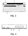
- Fig. 4 shows the support substrate 4, preferably a glass plate having sufficient strength, temperature-resistance and bending strength.
- a copper layer 5 and then the soldering tin 6 are applied to the support substrate 4 using methods known in semiconductor technology.
- connection between the support substrate 4 and the semiconductor circuit 1 can be seen from the diagram in Fig. 5 .
- either the support substrate 4 and/or the base 2 is heated to approximately 250°C, preferably by means of a heating plate, wherein the melting point of the soldering tin 6 is usually 218°C.
- a slight pressure is then exerted on the support substrate 4 and the base 2 so that the electrical contacts 3 dip into the soldering tin 6 without this leading to an electrical short-circuit between the electrical contacts 3 and the copper layer 5.
- the base 2 is then ground using suitable means and etched for example in potassium hydroxide (KOH) in order to uncover the actual semiconductor circuit 1, which is connected to the support substrate 4 via the electrical contacts 3.
- KOH potassium hydroxide
- a polymer layer 8 of the abovementioned polymers is likewise applied to its uncovered rear side, wherein the semiconductor circuit 1 is in this case upside down compared to the previous figures.
- the support substrate 4 can be heated again in order to release the soldered connection between the soldering tin 6 and the electrical contacts 3 and to place the semiconductor circuit 1 for example in a chip card.
Landscapes
- Wire Bonding (AREA)
- Die Bonding (AREA)
- Electric Connection Of Electric Components To Printed Circuits (AREA)
- Structures For Mounting Electric Components On Printed Circuit Boards (AREA)
- Container, Conveyance, Adherence, Positioning, Of Wafer (AREA)
- Bipolar Transistors (AREA)
- Mechanical Treatment Of Semiconductor (AREA)
Claims (7)
- Verfahren zum Abnehmen einer dünnen Halbleiterschaltung (1) von ihrer Basis (2), wobei die Halbleiterschaltung (1) mit Anschlüssen (3) zur elektrischen Kontaktierung, insbesondere mit Goldkontakten, versehen ist, dadurch gekennzeichnet, dass eine Schicht aus Lötzinn (6) auf ein Trägersubstrat (4) aufgebracht wird, das Trägersubstrat (4) mit den elektrischen Anschlüssen (3) verlötet wird, die Basis (2) der Halbleiterschaltung (1) abgenommen wird, und das Trägersubstrat (4) unter der Wirkung von Wärme wieder von der Halbleiterschaltung (1) abgenommen wird.
- Verfahren nach Anspruch 1, dadurch gekennzeichnet, dass Glas als Trägersubstrat verwendet wird.
- Verfahren nach Anspruch 1 oder 2, dadurch gekennzeichnet, dass eine Kupferschicht (5) zwischen dem Trägersubstrat (4) und dem Lötzinn (6) eingesetzt wird.
- Verfahren nach irgendeinem der Ansprüche 1 bis 3, dadurch gekennzeichnet, dass eine Polymerschicht (7) zwischen den elektrischen Anschlüssen (3) aufgebracht wird.
- Verfahren nach irgendeinem der Ansprüche 1 bis 4, dadurch gekennzeichnet, dass das Trägersubstrat (4) und die Halbleiterschaltung (1) unter Druck verlötet werden.
- Verfahren nach irgendeinem der Ansprüche 1 bis 5, dadurch gekennzeichnet, dass die Basis (2), insbesondere ein Silizium-Wafer, geschliffen und in Kaliumhydroxid (KOH) geätzt wird.
- Verfahren nach irgendeinem der Ansprüche 1 bis 6, dadurch gekennzeichnet, dass eine Polymerschicht (8) auf die Rückseite der Halbleiterschaltung (1) aufgebracht wird.
Priority Applications (1)
| Application Number | Priority Date | Filing Date | Title |
|---|---|---|---|
| EP05773837A EP1782462B1 (de) | 2004-08-20 | 2005-08-09 | Verfahren zum ablösen einer dünnen halbleiterschaltung von ihrer basis |
Applications Claiming Priority (3)
| Application Number | Priority Date | Filing Date | Title |
|---|---|---|---|
| EP04104002 | 2004-08-20 | ||
| EP05773837A EP1782462B1 (de) | 2004-08-20 | 2005-08-09 | Verfahren zum ablösen einer dünnen halbleiterschaltung von ihrer basis |
| PCT/IB2005/052635 WO2006018787A2 (en) | 2004-08-20 | 2005-08-09 | Method of detaching a thin semiconductor circuit from its base |
Publications (2)
| Publication Number | Publication Date |
|---|---|
| EP1782462A2 EP1782462A2 (de) | 2007-05-09 |
| EP1782462B1 true EP1782462B1 (de) | 2010-02-24 |
Family
ID=35559365
Family Applications (1)
| Application Number | Title | Priority Date | Filing Date |
|---|---|---|---|
| EP05773837A Expired - Lifetime EP1782462B1 (de) | 2004-08-20 | 2005-08-09 | Verfahren zum ablösen einer dünnen halbleiterschaltung von ihrer basis |
Country Status (7)
| Country | Link |
|---|---|
| US (1) | US8338228B2 (de) |
| EP (1) | EP1782462B1 (de) |
| JP (1) | JP2008511051A (de) |
| CN (1) | CN101044610A (de) |
| AT (1) | ATE459101T1 (de) |
| DE (1) | DE602005019581D1 (de) |
| WO (1) | WO2006018787A2 (de) |
Family Cites Families (9)
| Publication number | Priority date | Publication date | Assignee | Title |
|---|---|---|---|---|
| JP3116085B2 (ja) | 1997-09-16 | 2000-12-11 | 東京農工大学長 | 半導体素子形成法 |
| US6036809A (en) | 1999-02-16 | 2000-03-14 | International Business Machines Corporation | Process for releasing a thin-film structure from a substrate |
| JP2001185519A (ja) * | 1999-12-24 | 2001-07-06 | Hitachi Ltd | 半導体装置及びその製造方法 |
| US6444560B1 (en) * | 2000-09-26 | 2002-09-03 | International Business Machines Corporation | Process for making fine pitch connections between devices and structure made by the process |
| US6946314B2 (en) * | 2001-01-02 | 2005-09-20 | The Charles Stark Draper Laboratory, Inc. | Method for microfabricating structures using silicon-on-insulator material |
| DE10122324A1 (de) * | 2001-05-08 | 2002-11-14 | Philips Corp Intellectual Pty | Flexible integrierte monolithische Schaltung |
| US6797537B2 (en) | 2001-10-30 | 2004-09-28 | Irvine Sensors Corporation | Method of making stackable layers containing encapsulated integrated circuit chips with one or more overlaying interconnect layers |
| TWI229435B (en) | 2002-06-18 | 2005-03-11 | Sanyo Electric Co | Manufacture of semiconductor device |
| JP4575782B2 (ja) * | 2002-12-20 | 2010-11-04 | インターナショナル・ビジネス・マシーンズ・コーポレーション | 3次元デバイスの製造方法 |
-
2005
- 2005-08-09 AT AT05773837T patent/ATE459101T1/de not_active IP Right Cessation
- 2005-08-09 EP EP05773837A patent/EP1782462B1/de not_active Expired - Lifetime
- 2005-08-09 CN CNA200580035698XA patent/CN101044610A/zh active Pending
- 2005-08-09 DE DE602005019581T patent/DE602005019581D1/de not_active Expired - Lifetime
- 2005-08-09 JP JP2007526669A patent/JP2008511051A/ja not_active Withdrawn
- 2005-08-09 US US11/574,014 patent/US8338228B2/en active Active
- 2005-08-09 WO PCT/IB2005/052635 patent/WO2006018787A2/en not_active Ceased
Also Published As
| Publication number | Publication date |
|---|---|
| US8338228B2 (en) | 2012-12-25 |
| WO2006018787A3 (en) | 2006-08-17 |
| DE602005019581D1 (de) | 2010-04-08 |
| WO2006018787A2 (en) | 2006-02-23 |
| ATE459101T1 (de) | 2010-03-15 |
| EP1782462A2 (de) | 2007-05-09 |
| JP2008511051A (ja) | 2008-04-10 |
| CN101044610A (zh) | 2007-09-26 |
| US20090215226A1 (en) | 2009-08-27 |
Similar Documents
| Publication | Publication Date | Title |
|---|---|---|
| KR100540524B1 (ko) | 전자 부품 및 반도체 장치의 제조 방법, 반도체 장치, 회로기판 및 전자 기기 | |
| KR101173075B1 (ko) | 집적 회로 디바이스를 패키징하는 방법 및 장치 | |
| TW521356B (en) | Method of manufacturing IC device packages | |
| TW567738B (en) | Manufacturing method of circuit device and circuit device | |
| EP2224479B1 (de) | Metall-Keramik-Verbundsubstrat und Verfahren zu seiner Herstellung | |
| EP2006908B1 (de) | Elektronische Vorrichtung und dessen Herstellungsverfahren | |
| CN100474573C (zh) | 半导体装置及其制造方法 | |
| US20060163728A1 (en) | Semiconductor device and method for manufacturing semiconductor device | |
| US20080105952A1 (en) | Manufacturing method of semiconductor chips and semiconductor device having the semiconductor chips | |
| JP4219951B2 (ja) | はんだボール搭載方法及びはんだボール搭載基板の製造方法 | |
| EP2040294B1 (de) | Herstellungsverfahren für eine Halbleitervorrichtung | |
| US20220392817A1 (en) | Low cost reliable fan-out fan-in chip scale package | |
| EP0721661B1 (de) | Herstellungsmethode eines oberflächen-montierbaren bauteils und dieser selbst | |
| JP4452235B2 (ja) | パッケージ構造とその製造方法 | |
| US8232639B2 (en) | Semiconductor-device mounted board and method of manufacturing the same | |
| TW201019810A (en) | Low-temperature recoverable electronic component | |
| JP4215571B2 (ja) | 半導体装置の製造方法 | |
| US8338228B2 (en) | Method of detaching a thin semiconductor circuit from its base | |
| KR100501094B1 (ko) | 전자부품및반도체장치,및이들의제조방법 | |
| JP5238929B2 (ja) | 半導体装置及びその製造方法 | |
| EP2026380A2 (de) | Herstellungsverfahren für eine Halbleitervorrichtung | |
| JP2004079816A (ja) | チップ状電子部品の製造方法及びチップ状電子部品、並びにその製造に用いる疑似ウェーハの製造方法及び疑似ウェーハ、並びに実装構造 | |
| EP3692572A1 (de) | Struktur und verfahren für halbleiterpackung | |
| JP4286264B2 (ja) | 半導体装置及びその製造方法 | |
| JP2003152134A (ja) | チップ状電子部品の製造方法、及びその製造に用いる疑似ウェーハの製造方法 |
Legal Events
| Date | Code | Title | Description |
|---|---|---|---|
| PUAI | Public reference made under article 153(3) epc to a published international application that has entered the european phase |
Free format text: ORIGINAL CODE: 0009012 |
|
| 17P | Request for examination filed |
Effective date: 20070320 |
|
| AK | Designated contracting states |
Kind code of ref document: A2 Designated state(s): AT BE BG CH CY CZ DE DK EE ES FI FR GB GR HU IE IS IT LI LT LU LV MC NL PL PT RO SE SI SK TR |
|
| AX | Request for extension of the european patent |
Extension state: AL BA HR MK YU |
|
| RAP1 | Party data changed (applicant data changed or rights of an application transferred) |
Owner name: NXP B.V. |
|
| 17Q | First examination report despatched |
Effective date: 20090508 |
|
| GRAP | Despatch of communication of intention to grant a patent |
Free format text: ORIGINAL CODE: EPIDOSNIGR1 |
|
| GRAS | Grant fee paid |
Free format text: ORIGINAL CODE: EPIDOSNIGR3 |
|
| GRAA | (expected) grant |
Free format text: ORIGINAL CODE: 0009210 |
|
| AK | Designated contracting states |
Kind code of ref document: B1 Designated state(s): AT BE BG CH CY CZ DE DK EE ES FI FR GB GR HU IE IS IT LI LT LU LV MC NL PL PT RO SE SI SK TR |
|
| AX | Request for extension of the european patent |
Extension state: AL BA HR MK YU |
|
| REG | Reference to a national code |
Ref country code: GB Ref legal event code: FG4D |
|
| REG | Reference to a national code |
Ref country code: CH Ref legal event code: EP |
|
| REG | Reference to a national code |
Ref country code: IE Ref legal event code: FG4D |
|
| REF | Corresponds to: |
Ref document number: 602005019581 Country of ref document: DE Date of ref document: 20100408 Kind code of ref document: P |
|
| REG | Reference to a national code |
Ref country code: NL Ref legal event code: VDEP Effective date: 20100224 |
|
| LTIE | Lt: invalidation of european patent or patent extension |
Effective date: 20100224 |
|
| PG25 | Lapsed in a contracting state [announced via postgrant information from national office to epo] |
Ref country code: LT Free format text: LAPSE BECAUSE OF FAILURE TO SUBMIT A TRANSLATION OF THE DESCRIPTION OR TO PAY THE FEE WITHIN THE PRESCRIBED TIME-LIMIT Effective date: 20100224 Ref country code: IS Free format text: LAPSE BECAUSE OF FAILURE TO SUBMIT A TRANSLATION OF THE DESCRIPTION OR TO PAY THE FEE WITHIN THE PRESCRIBED TIME-LIMIT Effective date: 20100624 Ref country code: PT Free format text: LAPSE BECAUSE OF FAILURE TO SUBMIT A TRANSLATION OF THE DESCRIPTION OR TO PAY THE FEE WITHIN THE PRESCRIBED TIME-LIMIT Effective date: 20100625 |
|
| PG25 | Lapsed in a contracting state [announced via postgrant information from national office to epo] |
Ref country code: FI Free format text: LAPSE BECAUSE OF FAILURE TO SUBMIT A TRANSLATION OF THE DESCRIPTION OR TO PAY THE FEE WITHIN THE PRESCRIBED TIME-LIMIT Effective date: 20100224 Ref country code: PL Free format text: LAPSE BECAUSE OF FAILURE TO SUBMIT A TRANSLATION OF THE DESCRIPTION OR TO PAY THE FEE WITHIN THE PRESCRIBED TIME-LIMIT Effective date: 20100224 Ref country code: SI Free format text: LAPSE BECAUSE OF FAILURE TO SUBMIT A TRANSLATION OF THE DESCRIPTION OR TO PAY THE FEE WITHIN THE PRESCRIBED TIME-LIMIT Effective date: 20100224 Ref country code: AT Free format text: LAPSE BECAUSE OF FAILURE TO SUBMIT A TRANSLATION OF THE DESCRIPTION OR TO PAY THE FEE WITHIN THE PRESCRIBED TIME-LIMIT Effective date: 20100224 Ref country code: LV Free format text: LAPSE BECAUSE OF FAILURE TO SUBMIT A TRANSLATION OF THE DESCRIPTION OR TO PAY THE FEE WITHIN THE PRESCRIBED TIME-LIMIT Effective date: 20100224 |
|
| PG25 | Lapsed in a contracting state [announced via postgrant information from national office to epo] |
Ref country code: BE Free format text: LAPSE BECAUSE OF FAILURE TO SUBMIT A TRANSLATION OF THE DESCRIPTION OR TO PAY THE FEE WITHIN THE PRESCRIBED TIME-LIMIT Effective date: 20100224 Ref country code: CY Free format text: LAPSE BECAUSE OF FAILURE TO SUBMIT A TRANSLATION OF THE DESCRIPTION OR TO PAY THE FEE WITHIN THE PRESCRIBED TIME-LIMIT Effective date: 20100224 Ref country code: EE Free format text: LAPSE BECAUSE OF FAILURE TO SUBMIT A TRANSLATION OF THE DESCRIPTION OR TO PAY THE FEE WITHIN THE PRESCRIBED TIME-LIMIT Effective date: 20100224 Ref country code: ES Free format text: LAPSE BECAUSE OF FAILURE TO SUBMIT A TRANSLATION OF THE DESCRIPTION OR TO PAY THE FEE WITHIN THE PRESCRIBED TIME-LIMIT Effective date: 20100604 Ref country code: GR Free format text: LAPSE BECAUSE OF FAILURE TO SUBMIT A TRANSLATION OF THE DESCRIPTION OR TO PAY THE FEE WITHIN THE PRESCRIBED TIME-LIMIT Effective date: 20100525 Ref country code: NL Free format text: LAPSE BECAUSE OF FAILURE TO SUBMIT A TRANSLATION OF THE DESCRIPTION OR TO PAY THE FEE WITHIN THE PRESCRIBED TIME-LIMIT Effective date: 20100224 Ref country code: RO Free format text: LAPSE BECAUSE OF FAILURE TO SUBMIT A TRANSLATION OF THE DESCRIPTION OR TO PAY THE FEE WITHIN THE PRESCRIBED TIME-LIMIT Effective date: 20100224 Ref country code: SE Free format text: LAPSE BECAUSE OF FAILURE TO SUBMIT A TRANSLATION OF THE DESCRIPTION OR TO PAY THE FEE WITHIN THE PRESCRIBED TIME-LIMIT Effective date: 20100224 |
|
| PG25 | Lapsed in a contracting state [announced via postgrant information from national office to epo] |
Ref country code: CZ Free format text: LAPSE BECAUSE OF FAILURE TO SUBMIT A TRANSLATION OF THE DESCRIPTION OR TO PAY THE FEE WITHIN THE PRESCRIBED TIME-LIMIT Effective date: 20100224 Ref country code: SK Free format text: LAPSE BECAUSE OF FAILURE TO SUBMIT A TRANSLATION OF THE DESCRIPTION OR TO PAY THE FEE WITHIN THE PRESCRIBED TIME-LIMIT Effective date: 20100224 Ref country code: BG Free format text: LAPSE BECAUSE OF FAILURE TO SUBMIT A TRANSLATION OF THE DESCRIPTION OR TO PAY THE FEE WITHIN THE PRESCRIBED TIME-LIMIT Effective date: 20100524 |
|
| PLBE | No opposition filed within time limit |
Free format text: ORIGINAL CODE: 0009261 |
|
| STAA | Information on the status of an ep patent application or granted ep patent |
Free format text: STATUS: NO OPPOSITION FILED WITHIN TIME LIMIT |
|
| PG25 | Lapsed in a contracting state [announced via postgrant information from national office to epo] |
Ref country code: DK Free format text: LAPSE BECAUSE OF FAILURE TO SUBMIT A TRANSLATION OF THE DESCRIPTION OR TO PAY THE FEE WITHIN THE PRESCRIBED TIME-LIMIT Effective date: 20100224 |
|
| 26N | No opposition filed |
Effective date: 20101125 |
|
| PG25 | Lapsed in a contracting state [announced via postgrant information from national office to epo] |
Ref country code: IT Free format text: LAPSE BECAUSE OF FAILURE TO SUBMIT A TRANSLATION OF THE DESCRIPTION OR TO PAY THE FEE WITHIN THE PRESCRIBED TIME-LIMIT Effective date: 20100224 Ref country code: MC Free format text: LAPSE BECAUSE OF NON-PAYMENT OF DUE FEES Effective date: 20100831 |
|
| REG | Reference to a national code |
Ref country code: CH Ref legal event code: PL |
|
| PG25 | Lapsed in a contracting state [announced via postgrant information from national office to epo] |
Ref country code: CH Free format text: LAPSE BECAUSE OF NON-PAYMENT OF DUE FEES Effective date: 20100831 Ref country code: LI Free format text: LAPSE BECAUSE OF NON-PAYMENT OF DUE FEES Effective date: 20100831 |
|
| PG25 | Lapsed in a contracting state [announced via postgrant information from national office to epo] |
Ref country code: IE Free format text: LAPSE BECAUSE OF NON-PAYMENT OF DUE FEES Effective date: 20100809 |
|
| PG25 | Lapsed in a contracting state [announced via postgrant information from national office to epo] |
Ref country code: HU Free format text: LAPSE BECAUSE OF FAILURE TO SUBMIT A TRANSLATION OF THE DESCRIPTION OR TO PAY THE FEE WITHIN THE PRESCRIBED TIME-LIMIT Effective date: 20100825 Ref country code: LU Free format text: LAPSE BECAUSE OF NON-PAYMENT OF DUE FEES Effective date: 20100809 |
|
| PG25 | Lapsed in a contracting state [announced via postgrant information from national office to epo] |
Ref country code: TR Free format text: LAPSE BECAUSE OF FAILURE TO SUBMIT A TRANSLATION OF THE DESCRIPTION OR TO PAY THE FEE WITHIN THE PRESCRIBED TIME-LIMIT Effective date: 20100224 |
|
| PGFP | Annual fee paid to national office [announced via postgrant information from national office to epo] |
Ref country code: GB Payment date: 20120725 Year of fee payment: 8 |
|
| PGFP | Annual fee paid to national office [announced via postgrant information from national office to epo] |
Ref country code: DE Payment date: 20120723 Year of fee payment: 8 Ref country code: FR Payment date: 20120906 Year of fee payment: 8 |
|
| GBPC | Gb: european patent ceased through non-payment of renewal fee |
Effective date: 20130809 |
|
| PG25 | Lapsed in a contracting state [announced via postgrant information from national office to epo] |
Ref country code: DE Free format text: LAPSE BECAUSE OF NON-PAYMENT OF DUE FEES Effective date: 20140301 |
|
| REG | Reference to a national code |
Ref country code: FR Ref legal event code: ST Effective date: 20140430 |
|
| REG | Reference to a national code |
Ref country code: DE Ref legal event code: R119 Ref document number: 602005019581 Country of ref document: DE Effective date: 20140301 |
|
| PG25 | Lapsed in a contracting state [announced via postgrant information from national office to epo] |
Ref country code: GB Free format text: LAPSE BECAUSE OF NON-PAYMENT OF DUE FEES Effective date: 20130809 |
|
| PG25 | Lapsed in a contracting state [announced via postgrant information from national office to epo] |
Ref country code: FR Free format text: LAPSE BECAUSE OF NON-PAYMENT OF DUE FEES Effective date: 20130902 |