EP1783733A1 - Plasmaanzeigevorrichtung und Verfahren zu ihrer Ansteuerung - Google Patents
Plasmaanzeigevorrichtung und Verfahren zu ihrer Ansteuerung Download PDFInfo
- Publication number
- EP1783733A1 EP1783733A1 EP06251147A EP06251147A EP1783733A1 EP 1783733 A1 EP1783733 A1 EP 1783733A1 EP 06251147 A EP06251147 A EP 06251147A EP 06251147 A EP06251147 A EP 06251147A EP 1783733 A1 EP1783733 A1 EP 1783733A1
- Authority
- EP
- European Patent Office
- Prior art keywords
- data
- scan
- electrodes
- pulse
- electrode
- Prior art date
- Legal status (The legal status is an assumption and is not a legal conclusion. Google has not performed a legal analysis and makes no representation as to the accuracy of the status listed.)
- Withdrawn
Links
- 238000000034 method Methods 0.000 title claims description 64
- 238000006073 displacement reaction Methods 0.000 claims abstract description 129
- 230000009467 reduction Effects 0.000 abstract description 3
- 208000028659 discharge Diseases 0.000 description 125
- 210000004027 cell Anatomy 0.000 description 111
- 101001122448 Rattus norvegicus Nociceptin receptor Proteins 0.000 description 30
- 210000000712 G cell Anatomy 0.000 description 17
- 210000003719 b-lymphocyte Anatomy 0.000 description 17
- 238000010586 diagram Methods 0.000 description 8
- 102100024061 Integrator complex subunit 1 Human genes 0.000 description 6
- 101710092857 Integrator complex subunit 1 Proteins 0.000 description 6
- 102100033265 Integrator complex subunit 2 Human genes 0.000 description 6
- 108050002021 Integrator complex subunit 2 Proteins 0.000 description 6
- 102100033263 Integrator complex subunit 3 Human genes 0.000 description 6
- 101710092886 Integrator complex subunit 3 Proteins 0.000 description 6
- 238000010276 construction Methods 0.000 description 6
- 101100096319 Drosophila melanogaster Spc25 gene Proteins 0.000 description 5
- 238000013507 mapping Methods 0.000 description 5
- 230000004888 barrier function Effects 0.000 description 4
- 101150047356 dec-1 gene Proteins 0.000 description 4
- 238000010304 firing Methods 0.000 description 4
- 230000008878 coupling Effects 0.000 description 3
- 238000010168 coupling process Methods 0.000 description 3
- 238000005859 coupling reaction Methods 0.000 description 3
- 230000005855 radiation Effects 0.000 description 3
- 239000000758 substrate Substances 0.000 description 3
- 101150005267 Add1 gene Proteins 0.000 description 2
- 102100039134 Integrator complex subunit 4 Human genes 0.000 description 2
- 101710092887 Integrator complex subunit 4 Proteins 0.000 description 2
- 102100039131 Integrator complex subunit 5 Human genes 0.000 description 2
- 101710092888 Integrator complex subunit 5 Proteins 0.000 description 2
- 102100039133 Integrator complex subunit 6 Human genes 0.000 description 2
- 101710092889 Integrator complex subunit 6 Proteins 0.000 description 2
- 102100030147 Integrator complex subunit 7 Human genes 0.000 description 2
- 101710092890 Integrator complex subunit 7 Proteins 0.000 description 2
- 102100030148 Integrator complex subunit 8 Human genes 0.000 description 2
- 101710092891 Integrator complex subunit 8 Proteins 0.000 description 2
- 102100030206 Integrator complex subunit 9 Human genes 0.000 description 2
- 101710092893 Integrator complex subunit 9 Proteins 0.000 description 2
- 239000000470 constituent Substances 0.000 description 2
- 230000003247 decreasing effect Effects 0.000 description 2
- 239000007789 gas Substances 0.000 description 2
- 239000011261 inert gas Substances 0.000 description 2
- CPLXHLVBOLITMK-UHFFFAOYSA-N magnesium oxide Inorganic materials [Mg]=O CPLXHLVBOLITMK-UHFFFAOYSA-N 0.000 description 2
- 239000000395 magnesium oxide Substances 0.000 description 2
- AXZKOIWUVFPNLO-UHFFFAOYSA-N magnesium;oxygen(2-) Chemical compound [O-2].[Mg+2] AXZKOIWUVFPNLO-UHFFFAOYSA-N 0.000 description 2
- 230000000630 rising effect Effects 0.000 description 2
- 101150014859 Add3 gene Proteins 0.000 description 1
- 101100382321 Caenorhabditis elegans cal-1 gene Proteins 0.000 description 1
- OAICVXFJPJFONN-UHFFFAOYSA-N Phosphorus Chemical compound [P] OAICVXFJPJFONN-UHFFFAOYSA-N 0.000 description 1
- 101150060298 add2 gene Proteins 0.000 description 1
- 238000012937 correction Methods 0.000 description 1
- 230000006870 function Effects 0.000 description 1
- 238000007429 general method Methods 0.000 description 1
- 229910052734 helium Inorganic materials 0.000 description 1
- 239000001307 helium Substances 0.000 description 1
- SWQJXJOGLNCZEY-UHFFFAOYSA-N helium atom Chemical compound [He] SWQJXJOGLNCZEY-UHFFFAOYSA-N 0.000 description 1
- 238000009413 insulation Methods 0.000 description 1
- 239000000463 material Substances 0.000 description 1
- 239000007769 metal material Substances 0.000 description 1
- 238000012986 modification Methods 0.000 description 1
- 230000004048 modification Effects 0.000 description 1
- 229910052754 neon Inorganic materials 0.000 description 1
- GKAOGPIIYCISHV-UHFFFAOYSA-N neon atom Chemical compound [Ne] GKAOGPIIYCISHV-UHFFFAOYSA-N 0.000 description 1
- 238000013021 overheating Methods 0.000 description 1
- 229910052724 xenon Inorganic materials 0.000 description 1
- FHNFHKCVQCLJFQ-UHFFFAOYSA-N xenon atom Chemical compound [Xe] FHNFHKCVQCLJFQ-UHFFFAOYSA-N 0.000 description 1
Images











Classifications
-
- G—PHYSICS
- G09—EDUCATION; CRYPTOGRAPHY; DISPLAY; ADVERTISING; SEALS
- G09G—ARRANGEMENTS OR CIRCUITS FOR CONTROL OF INDICATING DEVICES USING STATIC MEANS TO PRESENT VARIABLE INFORMATION
- G09G3/00—Control arrangements or circuits, of interest only in connection with visual indicators other than cathode-ray tubes
- G09G3/20—Control arrangements or circuits, of interest only in connection with visual indicators other than cathode-ray tubes for presentation of an assembly of a number of characters, e.g. a page, by composing the assembly by combination of individual elements arranged in a matrix no fixed position being assigned to or needed to be assigned to the individual characters or partial characters
- G09G3/22—Control arrangements or circuits, of interest only in connection with visual indicators other than cathode-ray tubes for presentation of an assembly of a number of characters, e.g. a page, by composing the assembly by combination of individual elements arranged in a matrix no fixed position being assigned to or needed to be assigned to the individual characters or partial characters using controlled light sources
- G09G3/28—Control arrangements or circuits, of interest only in connection with visual indicators other than cathode-ray tubes for presentation of an assembly of a number of characters, e.g. a page, by composing the assembly by combination of individual elements arranged in a matrix no fixed position being assigned to or needed to be assigned to the individual characters or partial characters using controlled light sources using luminous gas-discharge panels, e.g. plasma panels
- G09G3/288—Control arrangements or circuits, of interest only in connection with visual indicators other than cathode-ray tubes for presentation of an assembly of a number of characters, e.g. a page, by composing the assembly by combination of individual elements arranged in a matrix no fixed position being assigned to or needed to be assigned to the individual characters or partial characters using controlled light sources using luminous gas-discharge panels, e.g. plasma panels using AC panels
- G09G3/291—Control arrangements or circuits, of interest only in connection with visual indicators other than cathode-ray tubes for presentation of an assembly of a number of characters, e.g. a page, by composing the assembly by combination of individual elements arranged in a matrix no fixed position being assigned to or needed to be assigned to the individual characters or partial characters using controlled light sources using luminous gas-discharge panels, e.g. plasma panels using AC panels controlling the gas discharge to control a cell condition, e.g. by means of specific pulse shapes
- G09G3/293—Control arrangements or circuits, of interest only in connection with visual indicators other than cathode-ray tubes for presentation of an assembly of a number of characters, e.g. a page, by composing the assembly by combination of individual elements arranged in a matrix no fixed position being assigned to or needed to be assigned to the individual characters or partial characters using controlled light sources using luminous gas-discharge panels, e.g. plasma panels using AC panels controlling the gas discharge to control a cell condition, e.g. by means of specific pulse shapes for address discharge
-
- G—PHYSICS
- G09—EDUCATION; CRYPTOGRAPHY; DISPLAY; ADVERTISING; SEALS
- G09G—ARRANGEMENTS OR CIRCUITS FOR CONTROL OF INDICATING DEVICES USING STATIC MEANS TO PRESENT VARIABLE INFORMATION
- G09G3/00—Control arrangements or circuits, of interest only in connection with visual indicators other than cathode-ray tubes
- G09G3/20—Control arrangements or circuits, of interest only in connection with visual indicators other than cathode-ray tubes for presentation of an assembly of a number of characters, e.g. a page, by composing the assembly by combination of individual elements arranged in a matrix no fixed position being assigned to or needed to be assigned to the individual characters or partial characters
- G09G3/22—Control arrangements or circuits, of interest only in connection with visual indicators other than cathode-ray tubes for presentation of an assembly of a number of characters, e.g. a page, by composing the assembly by combination of individual elements arranged in a matrix no fixed position being assigned to or needed to be assigned to the individual characters or partial characters using controlled light sources
- G09G3/28—Control arrangements or circuits, of interest only in connection with visual indicators other than cathode-ray tubes for presentation of an assembly of a number of characters, e.g. a page, by composing the assembly by combination of individual elements arranged in a matrix no fixed position being assigned to or needed to be assigned to the individual characters or partial characters using controlled light sources using luminous gas-discharge panels, e.g. plasma panels
- G09G3/288—Control arrangements or circuits, of interest only in connection with visual indicators other than cathode-ray tubes for presentation of an assembly of a number of characters, e.g. a page, by composing the assembly by combination of individual elements arranged in a matrix no fixed position being assigned to or needed to be assigned to the individual characters or partial characters using controlled light sources using luminous gas-discharge panels, e.g. plasma panels using AC panels
- G09G3/296—Driving circuits for producing the waveforms applied to the driving electrodes
-
- G—PHYSICS
- G09—EDUCATION; CRYPTOGRAPHY; DISPLAY; ADVERTISING; SEALS
- G09G—ARRANGEMENTS OR CIRCUITS FOR CONTROL OF INDICATING DEVICES USING STATIC MEANS TO PRESENT VARIABLE INFORMATION
- G09G3/00—Control arrangements or circuits, of interest only in connection with visual indicators other than cathode-ray tubes
- G09G3/20—Control arrangements or circuits, of interest only in connection with visual indicators other than cathode-ray tubes for presentation of an assembly of a number of characters, e.g. a page, by composing the assembly by combination of individual elements arranged in a matrix no fixed position being assigned to or needed to be assigned to the individual characters or partial characters
- G09G3/2007—Display of intermediate tones
- G09G3/2018—Display of intermediate tones by time modulation using two or more time intervals
- G09G3/2022—Display of intermediate tones by time modulation using two or more time intervals using sub-frames
-
- H—ELECTRICITY
- H01—ELECTRIC ELEMENTS
- H01J—ELECTRIC DISCHARGE TUBES OR DISCHARGE LAMPS
- H01J11/00—Gas-filled discharge tubes with alternating current induction of the discharge, e.g. alternating current plasma display panels [AC-PDP]; Gas-filled discharge tubes without any main electrode inside the vessel; Gas-filled discharge tubes with at least one main electrode outside the vessel
- H01J11/20—Constructional details
- H01J11/22—Electrodes, e.g. special shape, material or configuration
- H01J11/24—Sustain electrodes or scan electrodes
-
- G—PHYSICS
- G09—EDUCATION; CRYPTOGRAPHY; DISPLAY; ADVERTISING; SEALS
- G09G—ARRANGEMENTS OR CIRCUITS FOR CONTROL OF INDICATING DEVICES USING STATIC MEANS TO PRESENT VARIABLE INFORMATION
- G09G2310/00—Command of the display device
- G09G2310/02—Addressing, scanning or driving the display screen or processing steps related thereto
- G09G2310/0202—Addressing of scan or signal lines
- G09G2310/0213—Addressing of scan or signal lines controlling the sequence of the scanning lines with respect to the patterns to be displayed, e.g. to save power
-
- G—PHYSICS
- G09—EDUCATION; CRYPTOGRAPHY; DISPLAY; ADVERTISING; SEALS
- G09G—ARRANGEMENTS OR CIRCUITS FOR CONTROL OF INDICATING DEVICES USING STATIC MEANS TO PRESENT VARIABLE INFORMATION
- G09G2310/00—Command of the display device
- G09G2310/02—Addressing, scanning or driving the display screen or processing steps related thereto
- G09G2310/0202—Addressing of scan or signal lines
- G09G2310/0218—Addressing of scan or signal lines with collection of electrodes in groups for n-dimensional addressing
-
- G—PHYSICS
- G09—EDUCATION; CRYPTOGRAPHY; DISPLAY; ADVERTISING; SEALS
- G09G—ARRANGEMENTS OR CIRCUITS FOR CONTROL OF INDICATING DEVICES USING STATIC MEANS TO PRESENT VARIABLE INFORMATION
- G09G2330/00—Aspects of power supply; Aspects of display protection and defect management
- G09G2330/02—Details of power systems and of start or stop of display operation
- G09G2330/025—Reduction of instantaneous peaks of current
-
- G—PHYSICS
- G09—EDUCATION; CRYPTOGRAPHY; DISPLAY; ADVERTISING; SEALS
- G09G—ARRANGEMENTS OR CIRCUITS FOR CONTROL OF INDICATING DEVICES USING STATIC MEANS TO PRESENT VARIABLE INFORMATION
- G09G2330/00—Aspects of power supply; Aspects of display protection and defect management
- G09G2330/04—Display protection
- G09G2330/045—Protection against panel overheating
-
- G—PHYSICS
- G09—EDUCATION; CRYPTOGRAPHY; DISPLAY; ADVERTISING; SEALS
- G09G—ARRANGEMENTS OR CIRCUITS FOR CONTROL OF INDICATING DEVICES USING STATIC MEANS TO PRESENT VARIABLE INFORMATION
- G09G2360/00—Aspects of the architecture of display systems
- G09G2360/16—Calculation or use of calculated indices related to luminance levels in display data
Definitions
- the present invention relates to a display apparatus. It more particularly relates to a plasma display apparatus and driving method thereof.
- a conventional plasma display panel has a front panel and a rear panel.
- a barrier rib formed between the front panel and the rear panel forms one cell.
- Each cell is filled with an inert gas containing a primary discharge gas, such as neon (Ne), helium (He) or a mixed gas of Ne+He, and a small amount of xenon (Xe).
- a primary discharge gas such as neon (Ne), helium (He) or a mixed gas of Ne+He, and a small amount of xenon (Xe).
- a plurality of the cells forms one pixel. For example, a red (R) discharge cell, a green (G) discharge cell and a blue (B) discharge cell form one pixel.
- the inert gas when discharged with a high frequency voltage, it generates vacuum ultraviolet radiation.
- the vacuum ultraviolet radiation excites phosphors formed between the barrier ribs to emit visible light so as to display images.
- the plasma display apparatus can be made thin and light, and has thus been in the spotlight as the next-generation display device.
- a plurality of electrodes such as scan electrodes Y, sustain electrodes Z and address electrodes X, is formed in a plasma display panel. Predetermined driving voltages are applied to the plurality of electrodes to generate discharges, displaying images.
- a driver Integrated Circuit (IC) for supplying the driving voltages to the electrodes of the plasma display panel is connected to the electrodes.
- a data driver IC can be connected to the address electrodes X of the electrodes of the plasma display panel.
- a scan driver IC can be connected to the scan electrodes Y of the electrodes of the plasma display panel.
- a displacement current (Id) flows through the driver IC.
- the amount of the displacement current varies significantly due to a variety of factors.
- the displacement current flowing through the data driver IC can rise or fall depending on equivalent capacitance (C) of the plasma display panel and the switching number of the data driver IC. More particularly, the displacement current flowing through the data driver IC can increase as the equivalent capacitance (C) of the plasma display panel is increased and can also increase as the number of switching operations of the data driver increases.
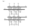
- the equivalent capacitance (C) of the plasma display panel can be determined by the equivalent capacitance (C) between electrodes. This will be described below with reference to the appended FIG. 1.
- FIG. 1 is a view illustrating equivalent capacitance of a plasma display panel.
- the equivalent capacitance (C) of the plasma display panel has equivalent capacitance (Cm1) between data electrodes, such as a data electrode X1 and a data electrode X2, equivalent capacitance (Cm2) between the data electrode and the scan electrode, such as the data electrode X1 and a scan electrode Y1, and equivalent capacitance (Cm2) between the data electrode and a sustain electrode, such as the data electrode X1 and a sustain electrode Z1.
- the state of a voltage applied to the scan electrode Y or the data electrode X is changed according to the operation of a switching element included in a drive IC, such as a scan drive IC, for driving the scan electrode Y by supplying a scan pulse to the scan electrode Y in an address period, and a drive IC, such as a data driver IC, for driving the data electrode X by supplying a data pulse to the data electrode X in an address period. Therefore, a displacement current (Id) generated by the equivalent capacitance (Cm1) and the equivalent capacitance (Cm2) flows through the data driver IC via the data electrode X.
- a displacement current (Id) generated by the equivalent capacitance (Cm1) and the equivalent capacitance (Cm2) flows through the data driver IC via the data electrode X.
- the amount of displacement current (Id) flowing through the data driver IC rises. Furthermore, if the number of switching operations (switching rate) of the data driver IC is increased, the amount of the displacement current (Id) rises.
- the switching rate of the data driver IC can vary depending on incoming image data.
- Embodiments of the present invention can provide a plasma display apparatus and driving method thereof in which electrical damage to a driver IC can be prevented.
- a plasma display apparatus comprises a plurality of scan electrodes, a plurality of data electrodes intersecting the scan electrodes, a scan driver arranged to supply scan pulses to the plurality of scan electrodes according to any one of two or more different scan pulse supply orders, and a data driver arranged to supply at least one data pulse, which corresponds to one scan pulse and has an application time point different from an application time point of the scan pulse, to the data electrodes.
- a plasma display apparatus comprises a plasma display panel in which a plurality of scan electrodes and a plurality of data electrodes intersecting the scan electrodes are formed, a scan driver arranged to supply a scan pulse to the scan electrodes by setting a scan order of the plurality of scan electrodes in a second data pattern different from a first data pattern of data patterns of incoming image data to be different from the scan order of the first data pattern, and a data driver arranged to supply at least one data pulse, which corresponds to one scan pulse and has an application time point different from an application time point of the scan pulse, to the data electrodes.
- a plasma display apparatus comprises a plurality of scan electrodes, a plurality of data electrodes intersecting the scan electrodes, a scan driver arranged to supply scan pulses to the plurality of scan electrodes according to any one of two or more different scan pulse supply orders, and a data driver arranged to supply at least one data pulse, which corresponds to one scan pulse and has an application time point different from an application time point of the scan pulse, to the data electrodes.
- the scan driver may supply the scan pulse according to the scan pulse supply order in which a displacement current of incoming image data is the lowest.
- the scan electrodes may comprise a first scan electrode and a second scan electrode
- the data electrodes may comprise a first data electrode and a second data electrode.
- a first discharge cell and a second discharge cell may be disposed at the intersections of the first scan electrode and the first and the second data electrodes.
- Third and fourth discharge cells may be disposed at the intersections of the second scan electrode and the first and the second data electrodes.
- the scan driver may calculate a displacement current for the first discharge cell by comparing data of the first to fourth discharge cells.
- the scan driver may obtain a first result of comparing data of the first discharge cell and data of the second discharge cell, a second result of comparing the data of the first discharge cell and data of the third discharge cell, and a third result of comparing the data of the third discharge cell and data of the fourth discharge cell, decide a calculation equation of the displacement current through a combination of the first to third results, and calculate a total displacement current of the first discharge cell by summing the displacement currents calculated using the decided calculation equation.
- the scan driver may calculate the displacement current according to a combination of the first to third results based on Cm1 and Cm2.
- the scan driver may calculate the displacement current of each sub-field of one frame, and may supply the scan pulse according to the scan pulse supply order in which the displacement current is the lowest each sub-field.
- the scan pulse supply order may comprise a first scan pulse supply order in which a scan pulse is supplied to the scan electrodes with them being divided into a plurality of groups.
- the scan driver may consecutively supply the scan pulse to scan electrodes belonging to the same scan electrode group in the case where a scan pulse supply order in which the displacement current is the lowest is the first scan pulse supply order.
- the scan driver may calculate a displacement current corresponding to each of the plurality of scan pulse supply orders according to incoming image data, and may supply the scan pulse to the scan electrodes according to at least one of scan pulse supply orders in which the displacement current is lower than a preset critical displacement current, of the plurality of scan pulse supply orders.
- the plurality of data electrodes may be divided into two or more data electrode groups.
- the data electrode groups may comprise one or more data electrodes.
- the data electrode groups may comprise the same number of data electrodes or a different number of data electrodes.
- the data driver may supply the data pulse to all of the data electrodes comprised in one data electrode group at the same application time point.
- the data driver may set a difference in an application time point between two or more data pulses corresponding to the one scan pulse to be the same or different.
- the data driver may set a difference in an application time point between two or more data pulses corresponding to the one scan pulse to range from 10 ns to 1000 ns.
- the data driver may set a difference in an application time point between two or more data pulses corresponding to the one scan pulse to have a value ranging from 1/100 to 1 times of a predetermined scan pulse width.
- a plasma display apparatus comprises a plasma display panel in which a plurality of scan electrodes and a plurality of data electrodes intersecting the scan electrodes are formed, a scan driver arranged to supply a scan pulse to the scan electrodes by setting a scan order of the plurality of scan electrodes in a second data pattern different from a first data pattern of data patterns of incoming image data to be different from the scan order of the first data pattern, and a data driver arranged to supply at least one data pulse, which corresponds to one scan pulse and has an application time point different from an application time point of the scan pulse, to the data electrodes.
- Any one of a data load value of the first data pattern and a data load value of the second data pattern may be more than a preset critical load value.
- a data load value depending on the data pattern may be obtained by the sum of a data load value in a horizontal direction of a data pattern and a data load value in a vertical direction of the data pattern.
- Any one of a displacement current of the first data pattern and a displacement current of the second data pattern may be more than a preset critical current.
- a plasma display apparatus and driving method thereof according to the present invention can be advantageous in that they can prevent the occurrence of excessive displacement current and can prevent electrical damage to a data driver IC accordingly.
- FIG. 1 is a view illustrating equivalent capacitance of a plasma display panel
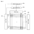
- FIG. 2 is a block diagram of a plasma display apparatus according to the present invention.
- FIGS. 3a and 3b are views illustrating an exemplary structure of a plasma display panel according to the present invention.
- FIG. 4 is a view illustrating a method of implementing gray levels of an image in a plasma display apparatus according to the present invention
- FIG. 5 is a view illustrating a method of driving a plasma display apparatus according to the present invention.
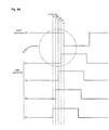
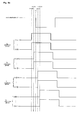
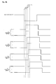
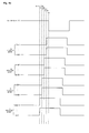
- FIGS. 6a to 6e are timing diagrams showing an example of a method of applying a data pulse to each data electrode at a different time point from an application time point of a scan pulse in the method of driving the plasma display apparatus according to the present invention
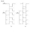
- FIGS. 7a and 7b are views illustrating noise reduced by a driving waveform according to the driving method of the present invention.
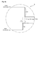
- FIG. 8 is a view illustrating that data electrodes are divided into four data electrode groups in order to explain another driving method of the plasma display apparatus according to the present invention.
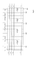
- FIGS. 9a to 9c illustrate examples in which data electrodes are divided into a plurality of electrode groups and a data pulse is applied to each electrode group at a different time point from an application time point of a scan pulse in the method of driving the plasma display apparatus according to the present invention
- FIG. 10 illustrates an example in which an application time point of a scan pulse and an application time point of a data pulse are set to be different from each other depending on each sub-field within a frame in the method of driving the plasma display apparatus according to the present invention
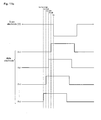
- FIGS. 11a to 11c are timing diagrams illustrating, in more detail, the driving waveform of FIG. 10;
- FIG. 12 is a view illustrating an amount of a displacement current depending on incoming image data
- FIGS.13a and 11b are views illustrating an exemplary method of changing a scan order considering image data and a displacement current accordingly;
- FIG. 14 is a view illustrating another application example in the method of driving the plasma display apparatus according to the present invention.
- FIG. 15 is a view illustrating, in detail, the construction and operation of a scan driver for realizing the method of driving the plasma display apparatus according to the present invention
- FIG. 16 shows a basic circuit block comprised in a data comparator included in the scan driver of the plasma display apparatus of the present invention
- FIG. 17 is a view illustrating, in more detail, the operation of first to third decision units of a data comparator
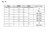
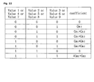
- FIG. 18 is a table showing pattern contents of image data depending on output signals of first to third decision units comprised in the basic circuit block of the data comparator according to the present invention.
- FIG. 19 is a block diagram illustrating a data comparator and a scan order decision unit of the scan driver in the plasma display apparatus of the present invention.
- FIG. 20 is a table showing pattern contents of image data depending on output signals of first to third decision units comprised in the data comparator of the present invention.
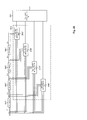
- FIG. 21 is a block diagram illustrating another construction of the basic circuit block comprised in the data comparator comprised in the scan driver of the plasma display apparatus according to the present invention.
- FIG. 22 is a table showing pattern contents of image data depending on output signals of first to ninth decision units comprised in the circuit block diagram of FIG. 21 according to the present invention.
- FIG. 23 is a block diagram illustrating a data comparator and a scan order decision unit of the scan driver in the plasma display apparatus of the present invention taking FIGS. 21 and 22 into consideration;
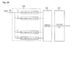
- FIG. 24 is a block diagram according to an embodiment in which the data comparator and the scan order decision unit according to the present invention are applied on a sub-field basis;
- FIG. 25 is a view illustrating an example of a method of selecting a sub-field for scanning scan electrodes according to any one of a plurality of scan pulse supply orders within one frame;
- FIG. 26 is a view illustrating that scan orders can be different from each other in patterns of two different image data
- FIG. 27 is a view illustrating an exemplary method of controlling a scan order by setting a critical value depending on an image data pattern
- FIG. 28 is a view illustrating an example of a method of deciding a scan order corresponding to scan electrode groups, each comprising a plurality of scan electrodes.
- a plasma display apparatus and driving method thereof according to an embodiment of the present invention will now be described with reference to FIG. 2.
- a plasma display apparatus comprises a plasma display panel 200, a data driver 201, a scan driver 202, a sustain driver 203, a sub-field mapping unit 204 and a data arrangement unit 205.
- the plasma display panel 200 has a front panel (not shown) and a rear panel (not shown), which are joined together with a predetermined distance therebetween.
- Data electrodes X intersecting the scan electrodes Y and the sustain electrode Z are also formed in the plasma display panel 200.
- the scan driver 202 supplies a ramp-up waveform (Ramp-up) and a ramp-down waveform (Ramp-down) to the scan electrodes Y during a reset period.
- the scan driver 202 also supplies a sustain pulse (SUS) to the scan electrodes Y during the sustain period. More particularly, the scan driver 202 scans the scan electrodes Y according to one of a plurality of scan pulse supply orders in which the order of supplying scan pulses to the plurality of scan electrodes Y in the address period is different. In other words, the scan driver 202 supplies a scan pulse (Sp) of a negative scan voltage (-Vy) to the scan electrodes Y during the address period according to one of the plurality of scan pulse supply orders.
- the sustain driver 203 supplies the sustain pulse (SUS) to the sustain electrode Z while operating alternately with the scan driver 202 during the sustain period, and provides a predetermined bias voltage (Vzb) to the sustain electrode Z in the address period and a set-down period.
- SUS sustain pulse
- Vzb predetermined bias voltage
- the sub-field mapping unit 204 sub-field-maps image data, which are supplied from the outside, e.g., from a halftone correction unit, and then outputs the sub-field mapped data.
- the data arrangement unit 205 rearranges the data that have been sub-field-mapped by the sub-field mapping unit 204 so that the data correspond to each of the data electrodes X of the plasma display panel 200.
- the data driver 201 samples and latches the data that have been rearranged by the data arrangement unit 205 under the control of a timing controller (not shown), and provides the resulting data to the data electrodes X. More particularly, the data driver 201 supplies the data to the data electrodes X corresponding to a scan pulse supply order in which the scan driver 202 scans the scan electrodes Y. The data driver 201 supplies data to the data electrodes corresponding to one scan pulse supply order, but supplies data pulses to one or more of the plurality of data electrodes at an application time point different from an application time point of a scan pulse applied to the scan electrodes by the scan driver 202.
- FIGS. 3a and 3b An example of a plasma display panel 200, i.e., one of the constituent elements of the plasma display apparatus of the present invention will now be described in more detail with reference to FIGS. 3a and 3b.
- the plasma display panel comprises a front panel 300 and a rear panel 310.
- a plurality of sustain electrodes in which a scan electrode 302, Y and a sustain electrode 303, Z are formed in pairs is arranged on a front substrate 301 serving as a display surface on which images are displayed.
- a plurality of data electrodes 313, X intersecting the plurality of sustain electrodes is arranged on a rear substrate 311 serving as a rear surface.
- the front panel 300 and the rear panel 310 are joined parallel to each other with a predetermined distance therebetween.
- the front panel 300 comprises pairs of the scan electrode 302, Y and the sustain electrode 303, Z, which mutually discharge and maintain the emission of a cell within one discharge cell.
- each of the scan electrode 302, Y and the sustain electrode 303, Z comprises a transparent electrode (a) formed of a transparent ITO material and a bus electrode (b) formed of a metal material.
- the scan electrode 302, Y and the sustain electrodes 303 Z are covered with one or more dielectric layers 304 for limiting discharge current and providing insulation between the electrode pairs.
- a protection layer 305 having deposited Magnesium Oxide (MgO) thereon is formed on the dielectric layers 304 in order to facilitate discharge conditions.
- MgO Magnesium Oxide
- barrier ribs 312 of a stripe form (or a well form), for forming a plurality of discharge spaces, i.e., discharge cells are arranged in parallel. Furthermore, the plurality of data electrodes 313, X, which perform an address discharge to generate vacuum ultraviolet radiation, is disposed parallel to the barrier ribs 312. R, G and B phosphor 314 that radiate visible light for displaying an image during the address discharge are coated on a top surface of the rear panel 310. A lower dielectric layer 315 for protecting the data electrodes 313, X is formed between the data electrodes 313, X and the phosphors 314.
- FIG. 3a shows only an exemplary structure of a plasma display panel, i.e., one of driving elements of the plasma display apparatus.
- the present invention is not limited to the structure of FIG. 3a.
- the scan electrode 302 Y and the sustain electrode 303, Z are formed in the front panel 300 and the data electrodes 313, X are formed in the rear panel 310.
- the scan electrode 302 Y, the sustain electrode 303 Z and the data electrodes 313 X can be formed in the front panel 300.
- each of the scan electrode 302, Y and the sustain electrode 303, Z comprises the transparent electrode (a) and the bus electrode (b). Unlike the above, however, one or more of the scan electrode 302, Y and the sustain electrode 303, Z can comprise only the bus electrode (b).
- FIG. 3a In the plasma display panel constructed as shown in FIG. 3a, the arrangement structure of the electrodes is shown in FIG. 3b.
- the scan electrodes Y and the sustain electrodes Z are parallel to each other.
- the data electrodes X cross the scan electrodes Y and the sustain electrodes Z.
- Drivers are connected to the electrodes.
- the plasma display apparatus including the plasma display panel, implements gray levels of various images with a frame being divided into a plurality of sub-fields.
- a method of implementing gray levels in the plasma display apparatus of the present embodiment will be described below with reference to FIG. 4. '
- one frame is divided into several sub-fields having a different durations of emissions.
- Each of the sub-fields is divided into a reset period (RPD) for initializing the entire cells, an address period (APD) for selecting a discharge cell to be discharged and a sustain period (SPD) for implementing gray levels depending on the number of discharges cycles and hence the respective durations of emission.
- RPD reset period
- APD address period
- SPD sustain period
- a frame period (16.67ms) corresponding to 1/60 seconds is divided into eight sub-fields (SF1 to SF8) as shown in FIG. 4.
- Each of the eight sub-fields (SF1 to SF8) is again divided into a reset period, an address period and a sustain period.
- the sustain period is a period where a gray level weight in each sub-field is decided.
- Gray levels of various images can be implemented by controlling the number of sustain pulses provided in a sustain period of each of sub-fields according to a gray level weight in the sustain period in each sub-field, as described above.
- one frame has eight sub-fields has been described in FIG. 4.
- the number of sub-fields constituting one frame can be varied in various manners. For example, one frame can has twelve sub-fields from a first sub-field to a twelfth sub-field. Ten sub-fields can also constitute one frame.
- sub-fields are arranged in order in which amounts of gray level weights increase in one frame. Unlike the above, however, sub-fields can be arranged in order in which amounts of gray level weights decrease in one frame, or can be arranged regardless of their gray level weights.
- a method of driving the plasma display apparatus in the address period of at least one sub-field, one or more of a plurality of data electrodes X are supplied with data pulses at an application time point different from an application time point of a scan pulse applied to the scan electrodes Y. Furthermore, though not shown in FIG. 5, a method of driving the plasma display apparatus can also include scanning the scan electrodes Y according to one of plurality of scan pulse supply orders in which an order of supplying the scan pulses to the plurality of scan electrodes Y in the address period is different. This will be described in detail with reference to FIG. 12 later on.
- a ramp-up waveform (Ramp-up) is applied to the scan electrode Y.
- the ramp-up waveform generates a weak dark discharge within discharge cells of the entire screen.
- the set-up discharge causes positive wall charges to be accumulated on the data electrode X and the sustain electrode Z and negative wall charges to be accumulated on the scan electrode Y.
- a ramp-down waveform (Ramp-down) which starts to fall from a positive voltage lower than a peak voltage of the ramp-up waveform to a predetermined voltage level lower than a ground (GND) level voltage, generates a weak erase discharge within the discharge cells, thus sufficiently erasing wall charges that have been excessively formed within the discharge cells.
- the set-down discharge causes wall charges of the degree in which an address discharge can be stably generated to uniformly remain within the discharge cells.
- sustain pulses are alternately applied to one or more of the scan electrode Y and the sustain electrode Z.
- a sustain discharge i.e., a display discharge is generated between the scan electrode Y and the sustain electrode Z in discharge cells selected by the address discharge whenever the sustain pulses are applied.
- a voltage of an erase ramp waveform (Ramp-ers) having a narrow pulse width and a low voltage level is applied to the sustain electrode Z in the erase period, thereby erasing wall charges remaining within the discharge cells of the entire screen.
- applying time points of a scan pulse and a data pulse are set to be different from each other.
- an application time point of the data pulse applied to the data electrodes X is set to be different from an application time point of the scan pulse applied to the scan electrode Y.
- the data pulse is applied to the data electrode X 1 at an application time point, which is 2 ⁇ t earlier than an application time point where the scan pulse is applied to the scan electrode Y, i.e., at an application time point ts-2 ⁇ t.
- the scan pulse is applied to the data electrode X 2 at an application time point, which is ⁇ t earlier than an application time point where the scan pulse is applied to the scan electrode Y, i.e., at an application time point ts- ⁇ t.
- the electrode X(n-1) is supplied with the data pulse at an application time point ts+ ⁇ t
- the electrode Xn is supplied with the data pulse at an application time point ts+2 ⁇ t. That is, as shown in FIG. 6a, the data pulse applied to the data electrodes X 1 to Xn is applied earlier than or later than the applying time points of the scan pulses applied to the scan electrodes Y.
- the data pulse is applied to the data electrode X 1 at an application time point, which is ⁇ t later than an application time point where the scan pulse is applied to the scan electrode Y, i.e., at an application time point ts+ ⁇ t.
- the scan pulse is applied to the data electrode X 2 at an application time point, which is 2 ⁇ t later than an application time point where the scan pulse is applied to the scan electrode Y, i.e., at an application time point ts+2 ⁇ t.
- the electrode X 3 is supplied with the data pulse at an application time point ts+3 ⁇ t
- the electrode Xn is supplied with the data pulse at an application time point ts+(n-1) ⁇ t. That is, as shown in FIG. 6b, the data pulses applied to the data electrodes X 1 to Xn are applied later than the applying time points of the scan pulses applied to the scan electrodes Y.
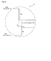
- a region A where a discharge in the driving waveform of FIG. 6b is generated will be described with reference to FIG. 6c.
- an address discharge firing voltage is 170V
- the voltage of the scan pulse is 100V
- a voltage of the data pulse is 70V.
- the voltage difference between the scan electrode Y and the data electrode X 1 becomes 100V due to the scan pulse applied to the scan electrode Y
- the voltage difference between the scan electrode Y and the data electrode X 1 rises up to 170V due to the data pulse applied to the data electrode X 1 after ⁇ t elapses since the scan pulse is applied. Therefore, since the voltage difference between the scan electrode Y and the data electrode X 1 becomes an address discharge firing voltage, an address discharge is generated between the scan electrode Y and the data electrode X 1 .
- the data pulse is applied to the data electrode X 1 at an application time point, which is ⁇ t earlier than an application time point where the scan pulse is applied to the scan electrode Y, i.e., at an application time point ts- ⁇ t.
- the scan pulse is applied to the data electrode X 2 at an application time point, which is 2 ⁇ t earlier than an application time point where the scan pulse is applied to the scan electrode Y, i.e., at an application time point ts-2 ⁇ t.
- the electrode X 3 is supplied with the data pulse at an application time point ts-3 ⁇ t
- the electrode Xn is supplied with the data pulse at an application time point ts-(n-1) ⁇ t. That is, as shown in FIG. 6d, the data pulses applied to the data electrodes X 1 to Xn are applied earlier than the applying time points of the scan pulses applied to the scan electrodes Y.
- a region B where a discharge in the driving waveform of FIG. 6d is generated will be described with reference to FIG. 6e.
- an address discharge firing voltage is 170V
- a voltage of the scan pulse is 100V
- a voltage of the data pulse is 70V as shown in FIG. 6c.
- a voltage difference between the scan electrode Y and the data electrode X 1 becomes 70V due to the data pulse applied to the electrode X 1
- a voltage difference between the scan electrode Y and the data electrodes X 1 to Xn rises up to 170V due to the scan pulse applied to the scan electrode Y after ⁇ t elapses since the data pulse is applied. Therefore, since the voltage difference between the scan electrode Y and the data electrode X 1 becomes an address discharge firing voltage, an address discharge is generated between the scan electrode Y and the data electrode X 1 .
- ⁇ t an application time point of the scan pulse applied to the scan electrode Y is ts
- the time difference in the application time point between data pulses, which are the closest to the applying time point ts of the scan pulse is ⁇ t
- the difference in an application time point between the applying time point ts of the scan pulse and a next data pulse is twice ⁇ t, i.e., 2 ⁇ t, wherein ⁇ t remains constant.
- the difference in the applying time point between the data pulses applied to the data electrodes X 1 to Xn is set to be the same.
- the difference in the applying time point between the data pulses applied to the data electrodes X 1 to Xn within one sub-field can be set to be the same, but the difference between an application time point of the scan pulse and the applying time points of data pulses, which are the closest to the applying time point of the scan pulse, can be set to be the same or different from each other.
- a time difference between the applying time point ts of the scan pulse and the application time point of a data pulse, which is the closest to the applying time point ts of the scan pulse can be set to 2 ⁇ t in other address periods in the same sub-field.
- the time difference between the applying time point ts of the scan pulse and the applying time point of the data pulse, which is the closest to the applying time point ts of the scan pulse can be set to range from 10 ns to 1000 ns when considering the limited time of the address period.
- ⁇ t can be set within a range of 1/100 to 1 times a predetermined scan pulse width. For example, assuming that the width of one scan pulse is 1 ⁇ s, the time difference between the applying time points can have 1/100 of 1 ⁇ s, i.e. from 10 ns to one times 1 ⁇ s, i.e., within a range of 1000 ns or less.
- the time difference in an application time point between the data pulses can also be set to be different from each other. That is, while the applying time points of the data pulses applied to the data electrodes X 1 to Xn are set to be different from the application time point of the scan pulse applied to the scan electrode Y, the applying time points of the data pulses applied to the data electrodes X 1 to Xn can be set to be different from each other.
- an application time point of the scan pulse applied to the scan electrode Y is ts and the time difference in the application time point between data pulses, which are the closest to the applying time point ts of the scan pulse is ⁇ t
- the difference between the applying time point ts of the scan pulse and an application time point of a data pulse, which is next to the applying time point ts of the scan pulse can be set to 3 ⁇ t.
- the application time point where the scan pulse is applied to the scan electrode Y is 0 ns
- the data pulse is applied to the data electrode X 1 at an application time point of 10 ns.
- the time difference between the applying time points of the scan pulses applied to the scan electrodes Y and the applying time point of the data pulse applied to the data electrode X 1 is 10 ns. Furthermore, a data pulse is applied to a next data electrode X 2 at an application time point of 20 ns. Therefore, the time difference between the applying time points of the scan pulses applied to the scan electrodes Y and the applying time point of the data pulse applied to the data electrode X 2 is 20 ns. As a result, the time difference between the applying time point of the scan pulse applied to the data electrode X 1 and the applying time point of the data pulse applied to the data electrode X 2 is 10 ns.
- a data pulse is applied to a next data electrode X 3 at an application time point of 40 ns. Therefore, the time difference between the applying time points of the scan pulses applied to the scan electrodes Y and the applying time point of the data pulse applied to the data electrode X 3 is 40 ns. As a result, the time difference between the applying time point of the scan pulse applied to the data electrode X 2 and the applying time point of the data pulse applied to the data electrode X 3 is 20 ns.
- the difference in the applying time point between the data pulses applied to the data electrodes X 1 to Xn can be set to be different.
- a time difference ⁇ t between the applying time points of the scan pulses applied to the scan electrodes Y and the applying time point of the data pulse applied to the data electrodes X 1 to Xn can be set to range from 10 ns to 1000 ns. Furthermore, from the viewpoint of a predetermined scan pulse width depending on the driving of the plasma display panel, ⁇ t can be set within a range of 1/100 to 1 times the predetermined scan pulse width.
- the application time point of the scan pulse applied to the scan electrode Y is set to be different from the applying time points of the data pulses applied to the data electrodes X 1 to Xn in the address period as described above, mutual capacitive coupling of the panel can be reduced at each of the applying time points of the data pulses applied to the data electrodes X 1 to Xn. It is thus possible to reduce noise of waveforms applied to the scan electrodes and the sustain electrodes.
- the noise which is generated in the waveforms applied to the scan electrode Y and the sustain electrode Z due to the data pulse applied to the data electrodes X in synchronization with the scan pulse applied to the scan electrode Y as described above, makes unstable an address discharge occurring in the address period. Therefore, a problem arises because driving efficiency of the plasma display panel is decreased.
- single scan method refers to a driving method in which the applying time points of scan waveforms applied to a number of scan electrodes formed on a display region of a front substrate are differently driven in each of the number of scan electrodes.
- the data electrodes X 1 to Xn of the plasma display panel 900 are divided into, e.g., a Xa electrode group (Xa 1 to Xa(n)/4) 901, a Xb electrode group (Xb((n/4)+1) to Xb(2n)/4) 902, a Xc electrode group (Xc((2n/4)+1) to Xc(3n)/4) 903 and a Xd electrode group (Xd((3n/4)+1) to Xd(n)) 904.
- At least one of the divided data electrode groups is supplied with the data pulse at an application time point different from an application time point of the scan pulse applied to the scan electrode Y. That is, the electrodes (Xa 1 to Xa(n)/4) belonging to the Xa electrode group 901 are supplied with the data pulses at different time points from the applying time points of the scan pulses applied to the scan electrodes Y, but the applying time points of the data pulses applied to the electrodes (Xa 1 to Xa(n)/4) belonging to the Xa electrode group 901 are the same.
- the electrodes belonging to the remaining electrode groups 902, 903 and 904 are supplied with the data pulses at time points different from the applying time points of the data pulses applied to the electrodes (Xa 1 to Xa(n)/4) belonging to the Xa electrode group 901.
- the applying time points of the data pulses applied to the electrodes belonging to the remaining data electrode groups 902, 903 and 904 can be the same as or different from the applying time points of the scan pulses applied to the scan electrodes Y.
- the number of the data electrodes included in each of the data electrode groups 901, 902, 903 and 904 is the same.
- the number of data electrodes included in each of the data electrode groups 901, 902, 903 and 904 can be set differently.
- the number of data electrode groups can also be changed.
- the number of data electrode groups can be set to range from 2 to a total number of the greatest data electrodes, i.e., 2 ⁇ N ⁇ (n-1).
- FIGS. 9a to 9c illustrate examples in which the data electrodes data electrodes X 1 to Xn are divided into a plurality of electrode groups and a data pulse is applied to each electrode group at an application time point different from an applying time of the scan pulse in the method of driving the plasma display apparatus.
- a plurality of data electrodes X 1 to Xn is divided into a plurality of data electrode groups (a Xa electrode group, a Xb electrode group, a Xc electrode group and a Xd electrode group) in the same manner as FIG. 8.
- applying time points of data pulses applied to the data electrodes X 1 to Xn of one ore more of the plurality of data electrode groups are different from an application time point of a scan pulse applied to a scan electrode Y.
- the applying time points of the scan pulses applied to the scan electrodes Y are set to be different from the applying time points of the data pulses applied to the data electrodes X 1 to Xn as described above, an address discharge can be prevented from becoming unstable and a decrease in driving stability can be prohibited accordingly. This results in enhanced driving efficiency.
- an application time point of a scan pulse applied to the scan electrode Y is ts.
- data pulses are applied to the data electrodes ((Xa 1 to Xa(n)/4) belonging to the Xa electrode group at an application time point, which is 2 ⁇ t earlier than an application time point where the scan pulse is applied to the scan electrode Y, i.e., at an application time point ts-2 ⁇ t.
- the scan pulse is applied to the data electrodes (Xb((n/4)+1) to Xb(2n)/4) belonging to the Xb electrode group at an application time point, which is ⁇ t earlier than an application time point where the scan pulse is applied to the scan electrode Y, i.e., at an application time point ts- ⁇ t.
- the data electrodes (Xc((2n/4)+1) to Xc(3n)/4) belonging to the Xc electrode group are supplied with the data pulses at an application time point ts+ ⁇ t
- the data electrodes (Xd((3n/4)+1) to Xd(n)) belonging to the Xd electrode group are supplied with the data pulses at an application time point ts+2 ⁇ t. That is, as shown in FIG. 9a, the data pulses applied to the electrode groups Xa, Xb, Xc and Xd, each having the data electrodes X 1 to Xn, are applied earlier than or later than the applying time points of the scan pulses applied to the scan electrodes Y.
- an application time point of the scan pulse applied to the scan electrode Y is ts.
- the data pulse are applied to the data electrodes included in the electrode group Xa at an application time point, which is ⁇ t later than an application time point where the scan pulse is applied to the scan electrode Y, i.e., at an application time point ts+ ⁇ t.
- the data pulses are applied to the data electrodes included in the electrode group Xb at an application time point, which is 2 ⁇ t later than an application time point where the scan pulse is applied to the scan electrode Y, i.e., at an application time point ts+2 ⁇ t.
- the data electrodes included in the electrode group Xc are supplied with the data pulses at an application time point ts+3 ⁇ t, and the data electrodes included in the electrode group Xc are supplied with the data pulses at an application time point ts+(n-1) ⁇ t. That is, as shown in FIG. 9b, the data pulses applied to the data electrode groups having data electrodes X 1 to Xn are applied later than the applying time points of the scan pulses applied to the scan electrodes Y.
- an application time point of the scan pulse applied to the scan electrode Y is ts.
- the data pulses are applied to the data electrodes included in the electrode group Xa at an application time point, which is ⁇ t earlier than an application time point where the scan pulse is applied to the scan electrode Y, i.e., at an application time point ts- ⁇ t.
- the data pulses are applied to the data electrodes included in the electrode group Xb at an application time point, which is 2 ⁇ t earlier than an application time point where the scan pulse is applied to the scan electrode Y, i.e., at an application time point ts-2 ⁇ t.
- the data electrodes included in the electrode group Xc are supplied with the data pulses at an application time point ts-3 ⁇ t, and the data electrodes included in the electrode group Xc are supplied with the data pulses at an application time point ts-(n-1) ⁇ t. That is, as shown in FIG. 9c, the data pulses applied to the data electrode groups having the data electrodes X 1 to Xn are applied earlier than the applying time points of the scan pulses applied to the scan electrodes Y.
- the difference in an application time point between the data electrode groups can be set to be the same or different as described above.
- FIG. 10 illustrates an example in which the applying time of a scan pulse and the applying time of a data pulse are set to be different from each other depending on each sub-field within a frame in a method of driving the plasma display apparatus.
- the time difference between applying time points of data pulses applied to the data electrodes X is the same, and the application time point of a scan pulse applied to the scan electrode Y and the applying time points of data pulses applied to the data electrodes X are different from each other. Furthermore, the time difference in an application time point between data pulses applied to the data electrodes X in an address period of at least one of sub-fields within one frame is different from the time difference in an application time point between data pulses applied to the data electrodes X in address periods of the remaining sub-fields.
- the time difference in the applying time point between the data pulses applied to the data electrodes is set to 2 ⁇ t.
- the time difference in the applying time point between the data pulses applied to the data electrodes can be set differently, such as 3 ⁇ t or 4 ⁇ t, on a sub-field basis included in one frame.
- the applying time points of the data pulses can be set differently on a sub-field basis prior to and subsequent to the applying time point of the scan pulse.
- the applying time points of some of the data pulses can be set prior to, and others subsequent to, the application time point of the scan pulse.
- the applying time points of all the data pulses can be set prior to the application time point of the scan pulse.
- the applying time points of all the data pulses can be set subsequent to the application time point of the scan pulse.
- the application time point of some of the data pulses applied to the data electrodes X 1 to Xn is prior to, and others subsequent to an application time point of the scan pulse applied to the scan electrode Y.
- the respective application time points of each of the data pulses applied to the data electrodes X 1 to Xn is different from the application time point of the scan pulse applied to the scan electrode Y, and the applying time points of all the data pulses are subsequent to the applying time point of the scan pulse.
- the applying time points of all the data pulses are shown as being set later than the applying time point of the scan pulse.
- the application time point of one data pulse can be set later than the applying time point of the scan pulse, and the number of data pulses that are applied later than the applying time point of the scan pulse can also be changed.
- the applying time points of the data pulses applied to the data electrodes X 1 to Xn are set to be different from the application time point of the scan pulse applied to the scan electrode Y, and the applying time points of all the data pulses are prior to the applying time point of the scan pulse.
- the applying time points of all the data pulses are shown as being set to be prior to the applying time point of the scan pulse.
- the application time point of one data pulse can be set to be prior to the applying time point of the scan pulse, and the number of data pulses that are applied prior to the applying time point of the scan pulse can also be changed.
- the data pulses are applied to the data electrodes X 1 to Xn at time points different from the application time point where the scan pulse is supplied, or according to arrangement sequence of the entire data electrodes, the data electrodes are divided into four electrode groups having the same number of data electrodes and the data pulses are applied on a electrode-group basis at time points different from an application time point where the scan pulse is applied.
- an alternative method is possible.
- odd-numbered data electrodes of the entire data electrodes X 1 to Xn can be set to one electrode group and even-numbered data electrodes of the entire data electrodes X 1 to Xn can be set to the other electrode group.
- the entire data electrodes within the same electrode group can be supplied with the data pulses at the same application time point, and the application time point of each of the data pulses of each electrode group can be set to be different from the application time point where the scan pulse is applied.
- the data electrodes X 1 to Xn are divided into a plurality of electrode groups at least one or more of which have a different number of data electrodes, and the data pulses are applied to each electrode group at an application time point different from the application time point of the scan pulse.
- the address electrode X 1 can be supplied with a data pulse at an application time point ts+ ⁇ t
- the data electrodes X 2 to X 10 can be supplied with data pulses at ts+3 ⁇ t
- the data electrodes X 11 to Xn can be supplied with data pulses at ts+4 ⁇ t, and the like.
- the method of driving the plasma display panel of the present invention can be modified in various ways.
- An order of scanning a plurality of scan electrodes Y in the address period which is one of major characteristics of the method of driving the plasma display apparatus, i.e., a method of scanning the scan electrodes Y according to one of a plurality of different scan pulse supply orders will be described below.
- a second scan electrode Y2 when a second scan electrode Y2 is scanned, i.e., when a scan pulse is supplied to the second scan electrode Y2, data electrodes, such as data electrodes X1 to Xm, are supplied with image data having an alternating logic value of 1 (high) and 0 (low). Furthermore, when a third scan electrode Y3 is scanned, the data electrodes X are kept to the logic value 0.
- the logic value 1 is a state where a voltage of the data pulse, i.e., a state where a data voltage (Vd) is applied to a corresponding data electrode X.
- the logic value 0 is a state where 0V is applied to a corresponding data electrode X, i.e., a state where the data voltage (Vd) is not applied.
- Id 1 / 2 ⁇ Cm ⁇ 1 + Cm ⁇ 2 ⁇ Vd
- Vd Voltage of data pulse applied to each data electrode X
- the logic value 0 is a state where 0V is applied to corresponding data electrodes X, i.e., a state where the data voltage (Vd) is not applied as described above.
- this corresponds a case where image data whose logic value is kept to 1 are supplied to a discharge cell on one scan electrode Y and image data whose logic value is kept to 0 are supplied to a discharge cell on a next scan electrode Y. Furthermore, this is true of a case where image data whose logic value is kept to 0 are supplied to a discharge cell on one scan electrode Y and image data whose logic value is kept to 1 are supplied to a discharge cell on a next scan electrode Y.
- Id 1 / 2 Cm ⁇ 2 ⁇ Vd
- Cm2 Equivalent capacitance between the data electrodes X and the scan electrodes Y or between the data electrodes X and the sustain electrodes Z
- Vd Voltage of the data pulse, which is applied to each of the data electrodes X
- the image data whose logic value is alternately changed between 1 and 0 are supplied to a discharge cell on one scan electrode Y.
- the image data whose logic value is alternately changed between 1 and 0 are supplied to a discharge cell on a next scan electrode Y so that the image data have a phase, which is shifted by 180° from the phase of the image data applied to the discharge cell on one scan electrode Y.
- the displacement current (Id) flowing through each of the data electrodes X can be expressed in the following Equation 3.
- Id 1 / 2 ⁇ 4 ⁇ Cm ⁇ 1 + Cm ⁇ 2 ⁇ Vd
- Cm2 Equivalent capacitance between the data electrodes X and the scan electrodes Y or between the data electrodes X and the sustain electrodes Z
- Vd Voltage of the data pulse, which is applied to each of the data electrodes X
- the image data whose logic value is alternately changed between 1 and 0 are supplied to the discharge cell on one scan electrode Y.
- the image data whose logic value is alternately changed between 1 and 0 are supplied to a discharge cell on a next scan electrode Y so that the image data have the same phase as that of the image data applied to the discharge cell on one scan electrode Y.
- Cm2 Equivalent capacitance between the data electrodes X and the scan electrodes Y or between the data electrodes X and the sustain electrodes Z
- Vd Voltage of the data pulse, which is applied to each of the data electrodes X
- image data whose logic value is kept to 0 are supplied to a discharge cell on one scan electrode Y, and image data whose logic value is kept to 0 are supplied to a discharge cell on a next scan electrode Y.
- the displacement current (Id) flowing through each of the data electrodes X can be expressed in the following Equation 5.
- Cm2 Equivalent capacitance between the data electrodes X and the scan electrodes Y or between the data electrodes X and the sustain electrodes Z
- Vd Voltage of the data pulse, which is applied to each of the data electrodes X
- the image data as shown in (c) of FIG. 12 correspond to the case where the number of switching operations of the data driver IC is the highest. Therefore, it can be seen that the greater the number of switching operations of the data driver IC, the greater the displacement current flowing through the data driver IC and the higher the possibility that the data driver IC may undergo electrical damage.
- FIGS.13a and 13b are views illustrating an example of a method of changing a scan order considering image data and a displacement current accordingly.
- FIGS. 13a and 13b show the same image data except for its scan order.
- the scan order of the scan electrodes Y is controlled according to the image data as shown in FIG. 13b, the amount of a displacement current flowing through the data driver IC can be reduced and the likelihood that the data driver IC may experience electrical damage will also be decreased.
- FIGS. 13a and 13b A method of driving the plasma display apparatus has been developed on the basis of the principle shown in FIGS. 13a and 13b. Another application example in a driving method of a plasma display apparatus will now be described with reference to FIG. 14.
- a method of driving a plasma display apparatus can perform scanning according to a selected one of four scan pulse supply orders, i.e., a first type (Type 1), a second type (Type 2), a third type (Type 3) and a fourth type (Type 4).
- scan pulses are supplied in an order in which the scan electrodes Y are arranged like Y1-Y2-Y3-...
- scan electrodes Y belonging to a first group are sequentially supplied with scan pulses
- scan electrodes Y belonging to a second group are sequentially supplied with scan pulses. That is, the scan electrodes Y1-Y3-Y5-, ..., Yn-1 are scanned and the scan electrodes Y2-Y4-Y6-, ..., Yn are scanned.
- scan electrodes Y belonging to a first group are sequentially supplied with scan pulses and scan electrodes Y belonging to a second group are sequentially supplied with scan pulses. Thereafter, scan electrodes Y belonging to a third group are sequentially supplied with scan pulses. That is, after the scan electrodes Y1-Y4-Y7-, ..., Yn-2 are scanned and the scan electrodes Y2-Y5-Y8-, ..., Yn-1 are scanned, the scan electrodes Y3-Y6-Y9-, ..., Yn are scanned.
- scan electrodes Y belonging to a first group are sequentially supplied with scan pulses and scan electrodes Y belonging to a second group are sequentially supplied with scan pulses. Thereafter, scan electrodes Y belonging to a third group are sequentially supplied with scan pulses, and scan electrodes Y belonging to a fourth group are sequentially supplied with scan pulses.
- FIG. 14 There has been shown in FIG. 14 only a method in which there are four kinds of scan pulse supply orders and the scan electrodes Y are scanned using a selected one of the four kinds of the scan pulse supply orders.
- the present invention is not limited to the above method.
- a method is possible in which there are various numbers of scan pulse supply orders, such as two kinds of scan pulse supply orders, three kinds of scan pulse supply orders and five kinds of scan pulse supply orders, and the scan electrodes Y are scanned using a selected one of them.
- the scan driver for implementing a method of driving a plasma display apparatus comprises a data comparator 1000 and a scan order decision unit 1001.
- the data comparator 1000 receives image data, which have been mapped by the sub-field mapping unit 204, and calculates the amount of a displacement current by comparing image data of a cell bundle consisting of one or more discharge cells located on a specific scan electrode Y line and image data of a cell bundle located in vertical and horizontal directions of the cell bundle using each of a plurality of scan pulse supply orders.
- cell bundle refers to that one or more cells are bundled to form one unit. For example, since R, G and B cells are bundled to form one pixel, a pixel corresponds to a cell bundle.
- the scan order decision unit 1001 decides a scan order using a scan pulse supply order having the lowest displacement current based on information about the amount of the displacement current, which has been calculated by the data comparator 1000.
- the data arrangement unit 205 rearranges the image data, which are sub-field mapped by the sub-field mapping unit 204, according the scan order decided by the above scan order decision unit 1001, and supplies the rearranged image data to the data electrodes X.
- the construction of the scan driver 202 shown in FIG. 15 will be described in conjunction with the aforementioned FIG. 14.
- the amount of displacement current with respect to the four kinds of the scan pulse supply orders in FIG. 14 is calculated by the data comparator 1000 of FIG. 15 and information about the amount of displacement current with respect to the four kinds of the scan pulse supply orders is provided to the scan order decision unit 1001.
- the scan order decision unit 1001 then compares the respective amounts of displacement current with respect to the four kinds of the scan pulse supply orders and selects one scan pulse supply order having the lowest displacement current.
- the scan order decision unit 1001 selects the fourth scan pulse supply order and decides a scan order of the scan electrodes Y according to the selected fourth scan pulse supply order.
- the scan order decision unit 1001 can select any one of the first, third and fourth scan pulse supply orders.
- information about the level of current which is sufficiently low enough not to cause electrical damage to the data driver IC can be set in advance. That is, the highest value of current, which is sufficiently low not to cause electrical damage to the data driver IC, is set as the critical current in advance.
- a scan pulse supply order where a displacement current lower than the critical current is generated can be selected.
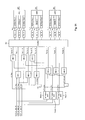
- a basic circuit block comprised in the data comparator 1000 of the scan driver comprises a memory unit 731, a first buffer buf1, a second buffer buf2, first to third decision units 734-1, 734-2 and 734-3, a decoder 735, first to third summation units 736-1, 736-2 and 736-3, first to third current calculators 737-1, 737-2 and 737-3, and a current summation unit 738.
- Image data corresponding to a (l-1) th scan electrode, i.e., a (l-1) th scan electrode line are stored in the memory unit 731.
- Image data corresponding to a l th scan electrode, i.e., a l th scan electrode line are input to the memory unit 731.
- the first buffer buf1 temporarily stores image data of a (q-1) th discharge cell of discharge cells corresponding to the l th scan electrode line.
- the second buffer buf2 temporarily stores image data of a (q-1) th discharge cell of discharge cells corresponding to the (l-1) th scan electrode line, which are stored in the memory unit 731.
- the first decision unit 734-1 comprises an XOR gate element, and it compares the image data of a q th discharge cell of the l th scan electrode line and the image data of the (q-1) th discharge cell of the l th scan electrode line, which are stored in the first buffer buf1. As a result of the comparison, if the two image data are different from each other, the first decision unit 734-1 outputs 1. If the two image data are identical to each other, the first decision unit 734-1 outputs 0.
- the second decision unit 734-2 comprises an XOR gate element, and it compares the image data of the q th discharge cell of the (l-1) th scan electrode line and the image data of the (q-1) th discharge cell of the (l-1) th scan electrode line, which are stored in the second buffer buf2. As a result of the comparison, if the two image data are different from each other, the second decision unit 734-2 outputs 1. If the two image data are identical to each other, the second decision unit 734-2 outputs 0.
- the third decision unit 734-3 comprises an XOR gate element, and it compares the image data of the (q-1) th discharge cell of the l th scan electrode line, which are stored in the first buffer buf1, and the image data of the (q-1) th discharge cell of the (l-1) th scan electrode line, which are stored in the second buffer buf2. As a result of the comparison, if the two image data are different from each other, the third decision unit 734-3 outputs 1. If the two image data are identical to each other, the third decision unit 734-3 outputs 0.
- FIG. 17 is a view illustrating, in more detail, the operation of first to third decision units of a data comparator. 1, 2 and 3 correspond to the operations of the first decision unit 734-1, the second decision unit 734-2 and the third decision unit 734-3, respectively.
- the data comparator 1000 compares image data of neighboring cells located in horizontal and vertical directions of one cell using the first decision unit 734-1 to the third decision unit 734-3, and then determines variations in the image data.
- the decoder 735 outputs a 3-bit signal corresponding to an output signal of each of the first to third decision units 734-1, 734-2 and 734-3.
- each of the first to third decision units 734-1, 734-2 and 734-3 is any one of (0,1,0), (0,1,1), (1,0,0) and (1,0,1), this is the same as the pattern state of the image data, which is shown in (a) of FIG. 13. Therefore, if the output signal is any one of (0,1,0), (0,1,1), (1,0,0) and (1,0,1), the displacement current (Id) is proportional to (Cm1+Cm2).
- first to third summation units 736-1, 736-2 and 736-3 of FIG. 16 sum output numbers of specific 3-bit signals output from the decoder 735, and output the summation result.
- the first summation unit 736-1 sums a number in which any one of (0,1,0), (0,1,1), (1,0,0) and (1,0,1) is output by the decoder 735 (C1).
- the second summation unit 736-2 sums a number in which (0,0,1) is output by the decoder 735 (C2).
- the third summation unit 736-3 sums a number in which (1,1,1) is output by the decoder 735 (C3).
- the first to third current calculators 737-1, 737-2 and 737-3 receive C1, C2 and C3 from the first summation unit 736-1, the second summation unit 736-2 and the third summation unit 736-3, respectively, and calculate amounts of the displacement current.
- the current summation unit 738 sums the amounts of the displacement current, which are calculated by the first to third current calculators 737-1, 737-2 and 737-3.
- the data comparator 1000 of the scan driver has a structure in which four basic circuit blocks shown in FIG. 19 are connected.
- the scan order decision unit 1001 compares the outputs of the four basic circuit blocks to decide a scan order that outputs the lowest displacement current.
- FIG. 19 corresponds to the case where a scan pulse supply order comprises a total of four scan pulse supply orders as in FIG. 14. That is, FIG. 19 shows the construction of the data comparator 1000 and the scan order decision unit 1001 corresponding to the case where the scan electrodes Y are scanned from the total of four scan pulse supply orders to one scan pulse supply order.
- the data comparator 1000 comprises first to fourth memory units 2001, 2003, 2005 and 2007, and first to fourth current decision units 2010, 2030, 2050 and 2070. That is, one memory unit and one current decision unit correspond to the basic circuit block shown in FIG. 16.
- the first to fourth memory units 2001, 2003, 2005 and 2007 are interconnected and store image data corresponding to the four scan electrode (Y) lines. That is, the first memory unit 2001 stores image data corresponding to a (l - 4) th scan electrode (Y) line.
- the second memory unit 2003 stores image data corresponding to a (l-3) th scan electrode (Y) line.
- the third memory unit 2005 stores image data corresponding to a (l-2) th scan electrode (Y) line.
- the fourth memory unit 907 stores image data corresponding to a (l-1) th scan electrode (Y) line.
- the first current decision unit 2010 receives the image data of the l th scan electrode (Y) line and the image data of the (l-4) th scan electrode (Y) line, which are stored in the first memory unit 2001. If the current of the first current decision unit 2010 that has received the image data is lower than the current of the second to fourth current decision units 2030, 2050 and 2070, the scan order is the same as the fourth scan pulse supply order (Type 4) of FIG. 14. That is, scanning has to be performed in order of Y1-Y5-Y9-, ..., Y2-Y6-Y10-, ..., Y3-Y7-Y11-, ..., Y4-Y8-Y12-, ....
- the operation of the first current decision unit 2010 is the same as that of the basic circuit block.
- the image data corresponding to the (l-4) th scan electrode (Y) line are stored in the first memory unit 2001, and the image data corresponding to the l th scan electrode (Y) line are input to the first memory unit 2001.
- the first buffer buf1 temporarily stores the image data of the (q-1) th discharge cell of the discharge cells corresponding to the l th scan electrode (Y) line.
- the first decoder Dec1 receives the output signals of the first to third decision units XOR1, XOR2 and XOR3 in parallel and then outputs 3-bit signals.
- an amount of capacitance that decides the amount of displacement current is varied depending on output signals (Value1, Value2, Value3) of the first to third decision units XOR1, XOR2 and XOR3.
- First to third summation units Int1, Int2 and Int3 sum output numbers of specific 3-bit signals, which are output from the first decoder Dec1, and output the sum results.
- the first summation unit Int1 sums (C1) a number in which any one of (0,0,1), (0,1,1), (1,0,0) and (1,1,0) is output by the first decoder Dec1.
- the second summation unit Int2 sums (C2) a number in which (0,1,0) is output by the first decoder Dec1.
- the third summation unit Int3 sums (C3) a number in which (1,1,1) is output by the first decoder Decl.
- First to third current calculators Call Cal2, Cal3 receive C1, C2 and C3 from the first summation units Int1, the second summation unit Int2 and the third summation unit Int3, respectively, and calculate amounts of the displacement current.
- the first current calculator Call calculates the amount of current by multiplying the output (C1) of the first summation unit Int1 and (Cm1+Cm2).
- the second current calculator Cal2 calculates the amount of current by multiplying the output (C2) of the second summation unit Int2 and Cm2.
- the third current calculator Cal3 calculates the amount of current by multiplying the output (C3) of the third summation unit Int3 and (4Cm1+Cm2).
- a first current summation unit Add1 sums the amounts of the displacement current, which are calculated by the first to third current calculators Cal1, Cal2 and Cal3.
- the second to fourth current decision units 2030, 2050 and 2070 also calculate the summed amounts of the displacement current.
- the first decision unit XOR1 of the second current decision unit 2030 comprises an XOR gate element, and it compares the image data (l, q) of the q th discharge cell of the l th scan electrode (Y) line and the image data (l, q-1) of the (q-1) th discharge cell of the l th scan electrode (Y) line, which are stored in the first buffer buf1. As a result of the comparison, if the two image data are different from each other, the first decision unit XOR1 outputs 1. If the two image data are identical to each other, the first decision unit XOR1 outputs 0.
- the second decision unit XOR2 of the second current decision unit 2030 comprises an XOR gate element, and it compares the image data (l, q-1) of the (q-1) th discharge cell of the l th scan electrode (Y) line and the image data (l-3, q-1) of the (q-1) th discharge cell of the (l-3) th scan electrode (Y) line, which are stored in the second buffer buf2. As a result of the comparison, if the two image data are different from each other, the second decision unit XOR2 outputs 1. If the two image data are identical to each other, the second decision unit XOR2 outputs 0.
- the third decision unit XOR3 of the second current decision unit 2030 comprises an XOR gate element, and it compares the image data (l-3, q-1) of the (q-1) th discharge cell of the (l-3) th scan electrode (Y) line, which are stored in the second buffer buf2, and the image data (l-3, q) of the q th discharge cell of the (l-3) th scan electrode (Y) line, which are output the second memory unit 2003. As a result of the comparison, if the two image data are different from each other, the third decision unit XOR3 outputs 1. If the two image data are identical to each other, the third decision unit XOR3 outputs 0.
- the first decision unit XOR1 of the third current decision unit 2050 comprises an XOR gate element, and it compares the image data (l, q) of the q th discharge cell of the l th scan electrode (Y) line and the image data (l, q-1) of the (q-1) th discharge cell of the l th scan electrode (Y) line, which are stored in the first buffer buf1. As a result of the comparison, if the two image data are different from each other, the first decision unit XOR1 outputs 1. If the two image data are identical to each other, the first decision unit XOR1 outputs 0.
- the second decision unit XOR2 of the third current decision unit 2050 comprises an XOR gate element, and it compares the image data (l, q-1) of the (q-1) th discharge cell of the l th scan electrode (Y) line and the image data (l-2, q-1) of the (q-1) th discharge cell of the (l-2) th scan electrode (Y) line, which are stored in the second buffer buf2. As a result of the comparison, if the two image data are different from each other, the second decision unit XOR2 outputs 1. If the two image data are identical to each other, the second decision unit XOR2 outputs 0.
- the third decision unit XOR3 of the third current decision unit 2050 comprises an XOR gate element, and it compares the image data (l-2, q-1) of the (q-1) th discharge cell of the (l-2) th scan electrode (Y) line, which are stored in the second buffer buf2, and the image data (l-2, q) of the q th discharge cell of the (l-2) th scan electrode (Y) line, which are output from the third memory unit 2005.
- the third decision unit XOR3 outputs 1. If the two image data are identical to each other, the third decision unit XOR3 outputs 0.
- the first decision unit XOR1 of the fourth current decision unit 2070 comprises an XOR gate element, and it compares the image data (l, q) of the q th discharge cell of the l th scan electrode (Y) line and the image data (l, q-1) of the (q-1) th discharge cell of the l th scan electrode (Y) line, which are stored in the first buffer buf1. As a result of the comparison, if the two image data are different from each other, the first decision unit XOR1 outputs 1. If the two image data are identical to each other, the first decision unit XOR1 outputs 0.
- the second decision unit XOR2 of the fourth current decision unit 2070 comprises an XOR gate element, and it compares the (q-1) th image data (l, q-1) of the l th scan electrode (Y) line and the image data (l-1, q-1) of the (q-1) th discharge cell of the (l-1) th scan electrode (Y) line, which are stored in the second buffer buf2. As a result of the comparison, if the two image data are different from each other, the second decision unit XOR2 outputs 1. If the two image data are identical to each other, the second decision unit XOR2 outputs 0.
- the third decision unit XOR3 of the fourth current decision unit 2070 comprises an XOR gate element, and it compares the image data (l-1, q-1) of the (q-1) th discharge cell of the (l-1) th scan electrode (Y) line, which are stored in the second buffer buf2, and the image data (l-1, q) of the q th discharge cell of the (l-1) th scan electrode (Y) line, which are output from the fourth memory unit 2007. As a result of the comparison, if the two image data are different from each other, the third decision unit XOR3 outputs 1. If the two image data are identical to each other, the third decision unit XOR3 outputs 0.
- the scan order decision unit 1001 receives the respective amounts of displacement current, which have been calculated by the first to fourth current decision units 2010, 2030, 2050 and 2070, and then decides a scan order according to the current decision unit that has output the lowest displacement current, or decides a scan order of the scan electrodes Y according to any one of the scan pulse supply orders, in which the displacement current lower than a previously set critical current is generated.
- the scan order decision unit 1001 determines that the amount of displacement current received from the second current decision unit 2030 is the lowest, the scan order decision unit 1001 sets a scan order so that scanning is performed in order of Y1-Y4-Y7-, ..., Y2-Y5-Y8-, ..., Y3-Y6-Y9-, ..., in the same manner as the third scan pulse supply order (Type 3) of FIG. 16.
- the scan order decision unit 1001 determines that the amount of displacement current received from the third current decision unit 2050 is the lowest, the scan order decision unit 1001 sets the scan order so that scanning is performed in order of Y1-Y3-Y5-, ..., Y2-Y4-Y6-, ..., in the same manner as the second scan pulse supply order (Type 2) of FIG. 16.
- the scan order decision unit 1001 determines that the amount of displacement current received from the fourth current decision unit 2070 is the lowest, the scan order decision unit 1001 sets the scan order so that scanning is performed in order of Y1-Y2-Y3-Y4-Y5-Y6-, ..., in the same manner as the first scan pulse supply order (Type 1) of FIG. 16.
- the basic circuit block comprised in the data comparator 1000 of the scan driver can be constructed differently from that of FIG. 16. This will be described below with reference to FIG. 21.
- the basic circuit block of FIG. 21 calculates the amount of the displacement current through variation in image data corresponding to R, G and B cells of a q th pixel and a (q-1) th pixel on the l th scan electrode line, variation in image data corresponding to R, G and B cells of the q th pixel and the (q-1) th pixel on the (l-1) th scan line, and variation in image data corresponding to R, G and B cells of the q th pixel on the l th scan electrode line and the (q-1) th pixel on the (l-1) th scan electrode line.
- First to third memory units Memory1, Memory2 and Memory3 temporarily store the image data corresponding to the R cell of the (l-1) th scan electrode line, the image data corresponding to the G cell of the (l-1) th scan electrode line, and the image data corresponding to the B cell of the (l-1) th scan electrode line, respectively.
- the first to third decision units XOR1, XOR2 and XOR3 decide variation between the image data corresponding to the R, G and B cells of the q th pixel on the l th scan electrode line.
- the first decision unit XOR1 compares image data (l, qR) corresponding to the R cell of the q th pixel on the l th scan electrode line and image data (l, qG) corresponding to the G cell of the q th pixel on the l th scan electrode line. As a result of the comparison, if the two data are different from each other, the first decision unit XOR1 outputs the logic value 1. If the two data are identical to each other, the first decision unit XOR1 outputs the logic value 0.
- the second decision unit XOR2 compares image data (l, qG) corresponding to the G cell of the q th pixel on the l th scan electrode line and image data (l, qB) corresponding to the B cell of the q th pixel on the l th scan electrode line. As a result of the comparison, if the two data are different from each other, the second decision unit XOR2 outputs the logic value 1. If the two data are identical to each other, the first decision unit XOR1 outputs the logic value 0.
- the third decision unit XOR3 compares image data (l, qB) corresponding to the B cell of the q th pixel on the l th scan electrode line and image data (l, q-1R) corresponding to the R cell of the (q-1) th pixel on the l th scan electrode line. As a result of the comparison, if the two data are different from each other, the third decision unit XOR3 outputs the logic value 1. If the two data are identical with each other, the first decision unit XOR1 outputs the logic value 0.
- the fourth to sixth decision units XOR4, XOR5 and XOR6 decide variation between the image data corresponding to the R, G and B cells of the q th pixel on the (l-1) th scan electrode line.
- the fourth decision unit XOR4 compares image data (l-1, qR) corresponding to the R cell of the q th pixel on the (l-1) th scan electrode line and image data (l-1, qG) corresponding to the G cell of the q th pixel on the (l-1) th scan electrode line. As a result of the comparison, if the two data are different from each other, the fourth decision unit XOR4 outputs the logic value 1. If the two data are identical with each other, the first decision unit XOR1 outputs the logic value 0.
- the fifth decision unit XOR5 compares image data (l-1, qG) corresponding to the G cell of the q th pixel on the (l-1) th scan electrode line and image data (l-1, qB) corresponding to the B cell of the q th pixel on the (l-1) th scan electrode line. As a result of the comparison, if the two data are different from each other, the fifth decision unit XOR5 outputs the logic value 1. If the two data are identical with each other, the first decision unit XOR1 outputs the logic value 0.
- the sixth decision unit XOR6 compares image data (l-1, qB) corresponding to the B cell of the q th pixel on the (l-1) th scan electrode line and image data (l-1, q-1R) corresponding to the R cell of the (q-1) th pixel on the (l-1) th scan electrode line. As a result of the comparison, if the two data are different from each other, the sixth decision unit XOR6 outputs the logic value 1. If the two data are identical with each other, the first decision unit XOR1 outputs the logic value 0.
- the seventh to ninth decision units XOR7, XOR8 and XOR9 decide variation between the image data by comparing the image data corresponding to the R, G and B cells of the q th pixel on the l th scan electrode line and the image data corresponding to the R, G and B cells of the q th pixel on the (l-1) th scan electrode line, respectively.
- the seventh decision unit XOR7 compares the image data (l, qR) corresponding to the R cell of the q th pixel on the l th scan electrode line and the image data (l-1, qR) corresponding to the R cell of the q th pixel on the (l-1) th scan electrode line. As a result of the comparison, if the two data are different from each other, the seventh decision unit XOR7 outputs the logic value 1. If the two data are identical with each other, the first decision unit XOR1 outputs the logic value 0.
- the eighth decision unit XOR8 compares the image data (l, qG) corresponding to the G cell of the q th pixel on the l th scan electrode line and the image data (l-1, qG) corresponding to the G cell of the q th pixel on the (l-1) th scan electrode line. As a result of the comparison, if the two data are different from each other, the eighth decision unit XOR8 outputs the logic value 1. If the two data are identical with each other, the first decision unit XOR1 outputs the logic value 0.
- the ninth decision unit XOR9 compares the image data (l, qB) corresponding to the B cell of the q th pixel on the l th scan electrode line and the image data (l-1, qB) corresponding to the B cell of the q th pixel on the (l-1) th scan electrode line. As a result of the comparison, if the two data are different from each other, the ninth decision unit XOR9 outputs the logic value 1. If the two data are identical with each other, the first decision unit XOR1 outputs the logic value 0.
- the decoder Dec outputs 3-bit signals corresponding to the output signals (Value1, Value2 and Value3) of the first to third decision units XOR1, XOR2 and XOR3, the output signals (Value4, Value5 and Value6) of the fourth to sixth decision units XOR4, XOR5 and XOR6, and the output signals (Value7, Value8 and Value9) of the seventh to ninth decision units XOR7, XOR8 and XOR9.
- the first to third summation units Int1, Int2 and Int3 sum (C1, C2, C3) the output numbers of the 3-bit signals, which are output from the decoder Dec and correspond to the output signals (Value1, Value2 and Value3) of the first to third decision units XOR1, XOR2 and XOR3, respectively, and then outputs the summation results.
- the fourth to sixth summation units Int4, Int5 and Int6 sum (C4, C5 and C6) the output numbers of the 3-bit signals, which are output from the decoder Dec and correspond to the output signals (Value4, Value5 and Value6) of the fourth to sixth decision units XOR4, XOR5 and XOR6, respectively, and then outputs the summation results.
- the seventh to ninth summation units Int7, Int8 and Int9 sum (C7, C8 and C9) the output numbers of the 3-bit signals, which are output from the decoder Dec and correspond to the output signals (Value7, Value8 and Value9) of the ninth decision units XOR7, XOR8 and XOR9, respectively, and then outputs the summation results.
- the first to third current calculators Call, Cal2 and Cal3 receive C1, C2 and C3 from the first, second and third summation units Int1, Int2 and Int3, respectively, and calculate amounts of displacement current.
- the fourth to sixth current calculators Cal4, Cal5 and Cal6 receive C4, C5 and C6 from the fourth, firth and sixth summation units Int4, Int5 and Int6, respectively, and calculate amounts of displacement current.
- the seventh to ninth current calculators Cal7, Cal8 and Cal9 receive C7, C8 and C9 from the seventh to ninth summation units Int7, Int8 and Int9, respectively, and calculate amounts of displacement current.
- the first current summation unit Add1 sums the amounts of displacement current, which are calculated by the first to third current calculators Call, Cal2 and Cal3.
- the second current summation unit Add2 sums the amounts of displacement current, which are calculated by the fourth to sixth current calculators Cal4, Cal5 and Cal6.
- the third current summation unit Add3 sums the amounts of displacement current, which are calculated by the seventh to ninth current calculators Cal7, Cal8 and Cal9.
- the amount of displacement current with respect to variation in image data corresponding to each cell can be calculated.
- the data comparator 1000 taking FIGS. 21 and 22 into consideration has a structure in which four basic circuit blocks shown in FIG. 23, i.e., first to fourth current decision units 2010', 2020', 2030' and 2040' are connected.
- the scan order decision unit 1001 compares the outputs of the four basic circuit blocks and decides a scan order that generates the lowest displacement current.
- the first current decision unit 2010' compares the image data (l, qR) and the image data (l, qG), the image data (l, qG) and the image data (l, qB), the image data (l, qB) and the image data (l, q-4R) , the image data (l-4, qR) and the image data (l-4, qG), the image data (l-4, qG) and the image data (l-4, qB), the image data (l-4, qB) and (l-4, q-1R), the image data (l, qR) and the image data (l-4, qR), the image data (l, qG) and (l-4, qG), and the image data (l, qB) and the image data (l-4, qB), respectively.
- l and l-4" refer to the l th scan electrode line and the (l-4) th scan electrode line, respectively.
- qR”, “qG” and “qB” refer to the R, G and B cells of the q th pixel, respectively.
- q-1R, “q-1G” and “q-1B” refer to the R, G and B cells of the (q-1) th pixel, respectively.
- the first current decision unit 2010' compares the image data and calculates an amount of the displacement current, which corresponds to the scan order of Type 4 as described above.
- the second current decision unit 2020' compares the image data (l, qR) and the image data (l, qG), the image data (l, qG) and the image data (l, qB), the image data (l, qB) and the image data (l, q-1R), the image data (l-3, qR) and the image data (l-3, qG), the image data (l-3, qG) and the image data (l-3, qB), the image data (l-3, qB) and (l-3, q-1R), the image data (l, qR) and the image data (l-3, qR), the image data (l, qG) and (l-3, qG), and the image data (l, qB) and the image data (l-3, qB), respectively.
- l and (l-3) refer to the l th scan electrode line and the (l-3) th scan electrode line, respectively.
- the second current decision unit 2020' compares the image data and calculates the amount of displacement current, which corresponds to the scan order of Type 3, as described above.
- the third current decision unit 2030' compares the image data (l, qR) and the image data (l, qG), the image data (l, qG) and the image data (l, qB), the image data (l, qB) and the image data (l, q-1R), the image data (l-2, qR) and the image data (l-2, qG), the image data (l-2, qG) and the image data (l-2, qB), the image data (l-2, qB) and (l-2, q-1R), the image data (l, qR) and the image data (l-2, qR), the image data (l, qG) and the image data (l-2, qG), and the image data (l, qB) and the image data (l-2, qB), respectively.
- l and (l-2) refer to the l th scan electrode line and the (l-2) th scan electrode line, respectively.
- the third current decision unit 2030' compares the image data and calculates the amount of displacement current, which corresponds to the scan order of Type 2 as described above.
- the fourth current decision unit 2040' compares the image data (l, qR) and the image data (l, qG), the image data (l, qG) and the image data (l, qB), the image data (l, qB) and the image data (l, q-1R), the image data (l-1, qR) and the image data (l-1, qG), the image data (l-1, qG) and the image data (l-1, qB), the image data (l-1, qB) and the image data (l-1, q-1R), the image data (l, qR) and the image data (l-1, qR), the image data (l, qG) and (l-1, qG), and the image data (l, qB) and the image data (l-1, qB), respectively.
- l and (l-1) refer to the l th scan electrode line and the (l-1) th scan electrode line, respectively.
- the fourth current decision unit 2040' compares the image data and calculates the amount of displacement current, which corresponds to the scan order of Type 1, as described above.
- the scan order decision unit 1001 receives the amounts of displacement current, which are calculated by the first to fourth current decision units 2010', 2030', 2050' and 2070', and decides a scan order according to the current decision unit that has output the lowest displacement current.
- the scan order decision unit 1001 determines that the amount of displacement current, which is received from the second current decision unit 2030', is the lowest, the scan order decision unit 1001 sets the scan order so that scanning is performed in order of Y1-Y4-Y7-, ..., Y2-Y5-Y8-, ..., Y3-Y6-Y9- ..., in the same manner as the third scan pulse supply order (Type 3) of FIG. 21.
- the scan order decision unit 1001 determines that the amount of displacement current, which is received from the third current decision unit 2050', is the lowest, the scan order decision unit 1001 sets the scan order so that scanning is performed in order of Y1-Y3-Y5-, ..., Y2-Y4-Y6-, ..., in the same manner as the second scan pulse supply order (Type 2) of FIG. 14.
- each of a data comparator for a first sub-field (SF1) to a data comparator for a sixteenth sub-field (SF16) calculates an amount of displacement current according to an image pattern in a corresponding sub-field with respect to a plurality of scan pulse supply orders, and stores the calculated amount in a buffer 800.
- Each data comparator for the first sub-field (SF1) to the data comparator for the sixteenth sub-field (SF16) is the same as the block construction of the data comparator shown in FIG. 19.
- Each data comparator for the first sub-field (SF1) to the data comparator for the sixteenth sub-field (SF16) calculates an amount of displacement current according to the pattern of image data in each sub-field with respect to a plurality of scan pulse supply orders, and stores the calculated amount in the buffer 800.
- the scan order decision unit 1001 compares the respective amounts of displacement current according to the patterns of the image data for the respective sub-fields, which are received from the buffer 800, recognises the pattern of image data having the lowest displacement current, and decides a scan order every sub-field.
- the respective displacement current between the scan electrode lines corresponding to a plurality of scan pulse supply orders are calculated, and lines corresponding to the scan pulse supply orders having the lowest displacement current are sequentially scanned.
- a displacement current between lines in which scan pulse supply orders are spaced apart from one another at regular intervals by a predetermined number is calculated, and the scan pulse supply order having the lowest displacement current is selected.
- a displacement current between lines in which scan pulse supply orders are spaced apart from one another irregularly or according to a predetermined rule can be calculated, and the scan pulse supply order having the lowest displacement current can be selected.
- the displacement current is calculated using weights (Cm2, Cm1+ Cm2, or 4Cm1+Cm2), which comprise at least one of capacitances (Cm1 and Cm2).
- the respective amounts of displacement currents of the sub-fields can be found by summing the values of "u0"v or "u1”v in such a manner that in the case where weights are not used and displacement current does not flow, the amount of displacement current is set to "u0"v and in the case where displacement current flows, the amount of displacement current is set to "u1"v.
- the first to third summation units 736-1 to 736-3 can be constructed using one summation unit, and the current calculators 737-1 to 737-3 and the current summation unit 738 may be omitted. In this case, one summation unit can count the output numbers of C1, C2 and C3 and calculate the count values themselves as displacement currents.
- the scan electrodes Y are scanned using the first scan pulse supply order (Type 1) of FIG. 14 only in a first sub-field having the lowest gray level weight, of sub-fields comprised in one frame, and the scan electrodes Y are scanned according to a general method, i.e., a sequential scanning method in the remaining sub-fields.
- the displacement current for a plurality of scan pulse supply orders is calculated in respective selected one or more of sub-fields comprised in one frame, and the scan electrodes Y are then scanned using a scan pulse supply order in which the displacement current is the lowest in each sub-field.
- the displacement current with respect to the plurality of scan pulse supply orders are calculated in the respective sub-fields comprised in one frame, and the scan electrodes Y are scanned according to a scan pulse supply order in which the displacement current is the lowest in each sub-field, as shown in FIG. 24.
- patterns of image data comprise a first pattern and a second pattern
- the scan order in the first pattern of the image data and the scan order in the second pattern of the image data can be different from each other. This will be described in more detail with reference to FIG. 26.
- (a) shows a pattern of image data, in which the logic level “1” and the logic level “0” are alternately disposed in up and down directions and right and left directions.
- (b) shows a pattern of image data, in which the logic levels “1” and “0” are alternately disposed in right and left directions, but the logic levels “1” and “0” are not changed in up and down directions.
- the scan order of the scan electrodes Y is Y1-Y3-Y5-Y7-Y2-Y4-Y6.
- the scan order of the scan electrodes Y is Y1-Y2-Y3-Y4-Y5-Y6-Y7. That is, the scan order of the scan electrodes Y is different in the case where the image data have the pattern as shown in (a) and the image data have the pattern as shown in (b).
- FIG. 27 shows a case where image data are all high level, i.e., the logic level "1".
- (b) of FIG. 27 shows a case where image data are all the logic level "1" on Y1, Y2 and Y3 scan electrode lines and are all the logic level "0" on a Y4 scan electrode line.
- (c) of FIG. 27 shows a case where the first and second of Y1 and Y2 scan electrodes are the logic level "1” and the third and fourth of the Y1 and Y2 scan electrodes are the logic level "0", and image data are all the logic level "1” on Y3 and Y4 scan electrode lines.
- (d) of FIG. 27 shows a case where the logic levels "1” and "0" are alternately disposed.
- the load value is the sum of a load value in the horizontal direction of a corresponding data pattern and a load value in the vertical direction of a corresponding data pattern.
- a previously set critical load value is a load depending on a total number of ten switchings in up and down directions and a total number of ten switchings in right and left directions, only the case of the last pattern (d) of the patterns (a), (b), (c) and (d) exceeds the previously set critical load value.
- the scan order of the scan electrodes Y can be controlled.
- the control of the scan order of the scan electrodes Y has already been described in detail. Description thereof will be omitted in order to avoid redundancy.
- each scan electrode group is set to comprise four scan electrodes. It is, however, to be understood that other groupings are possible.
- one or more of a plurality of scan electrode groups can be set to comprise a different number of scan electrodes Y from the remaining scan electrode groups.
- two scan electrodes Y can be comprised in a first scan electrode group and four scan electrodes Y can be comprised in a second scan electrode group.
- the scan electrode groups are set as described above, if the second type (Type 2) of FIG. 14 is applied, the third scan electrode group is scanned after scanning the first scan electrode group and the second and fourth scan electrode groups are then sequentially scanned, as in FIG. 28.
- the scan order is Y1, Y2, Y3, Y7, Y8, Y9, Y4, Y5, Y6, Y10, Y11 and Y12.
Landscapes
- Engineering & Computer Science (AREA)
- Physics & Mathematics (AREA)
- Computer Hardware Design (AREA)
- General Physics & Mathematics (AREA)
- Theoretical Computer Science (AREA)
- Plasma & Fusion (AREA)
- Power Engineering (AREA)
- Chemical & Material Sciences (AREA)
- Materials Engineering (AREA)
- Control Of Indicators Other Than Cathode Ray Tubes (AREA)
- Control Of Gas Discharge Display Tubes (AREA)
Applications Claiming Priority (1)
| Application Number | Priority Date | Filing Date | Title |
|---|---|---|---|
| KR1020050106205A KR100829019B1 (ko) | 2005-11-07 | 2005-11-07 | 플라즈마 디스플레이 장치 및 그의 구동 방법 |
Publications (1)
| Publication Number | Publication Date |
|---|---|
| EP1783733A1 true EP1783733A1 (de) | 2007-05-09 |
Family
ID=36922082
Family Applications (1)
| Application Number | Title | Priority Date | Filing Date |
|---|---|---|---|
| EP06251147A Withdrawn EP1783733A1 (de) | 2005-11-07 | 2006-03-02 | Plasmaanzeigevorrichtung und Verfahren zu ihrer Ansteuerung |
Country Status (5)
| Country | Link |
|---|---|
| US (1) | US20070103390A1 (de) |
| EP (1) | EP1783733A1 (de) |
| JP (1) | JP2007133348A (de) |
| KR (1) | KR100829019B1 (de) |
| CN (1) | CN100504987C (de) |
Cited By (2)
| Publication number | Priority date | Publication date | Assignee | Title |
|---|---|---|---|---|
| EP2065876A2 (de) | 2007-11-28 | 2009-06-03 | Samsung SDI Co., Ltd. | Plasmaanzeigevorrichtung und Verfahren zu ihrer Ansteuerung |
| EP2192569A1 (de) | 2008-12-01 | 2010-06-02 | Samsung SDI Co., Ltd. | Plasmaanzeige und Verfahren zu ihrer Ansteuerung |
Families Citing this family (7)
| Publication number | Priority date | Publication date | Assignee | Title |
|---|---|---|---|---|
| KR101174722B1 (ko) * | 2007-09-20 | 2012-08-21 | 주식회사 오리온 | 플라즈마 디스플레이 패널 구동방법 |
| KR20090078532A (ko) * | 2008-01-15 | 2009-07-20 | 삼성에스디아이 주식회사 | 플라즈마 표시 장치 및 그 구동 방법 |
| KR100998092B1 (ko) * | 2008-12-08 | 2010-12-03 | 삼성에스디아이 주식회사 | 접촉 장치 및 그를 포함하는 플라즈마 표시 장치 및 그 구동 방법 |
| KR20140071688A (ko) * | 2012-12-04 | 2014-06-12 | 삼성디스플레이 주식회사 | 표시장치 및 그의 구동방법 |
| CN104036744B (zh) * | 2014-06-07 | 2016-04-13 | 深圳市华星光电技术有限公司 | 一种显示器的驱动方法及装置 |
| KR102425982B1 (ko) * | 2015-09-25 | 2022-07-28 | 삼성디스플레이 주식회사 | 표시 패널의 구동 방법 및 이를 수행하는 표시 장치 |
| CN108735164B (zh) * | 2017-04-20 | 2020-10-23 | 合肥捷达微电子有限公司 | 电子纸显示装置及其显示驱动系统与显示驱动方法 |
Citations (5)
| Publication number | Priority date | Publication date | Assignee | Title |
|---|---|---|---|---|
| EP0853306A1 (de) * | 1997-01-10 | 1998-07-15 | Nec Corporation | Verfahren für Spitzenstromreduzierung für eine Plasmaanzeigeeinrichtung |
| EP0945844A2 (de) * | 1998-03-26 | 1999-09-29 | Fujitsu Limited | Anzeigegerät und Steuerverfahren dafür |
| US20010024179A1 (en) * | 2000-03-23 | 2001-09-27 | Tadashi Nakamura | Plasma display with reduced power consumption |
| WO2001082284A1 (en) * | 2000-04-26 | 2001-11-01 | Ultrachip, Inc. | Low power lcd driving scheme |
| US20050184929A1 (en) * | 2004-02-19 | 2005-08-25 | Soo-Jin Lee | Apparatus for driving plasma display panel and method for displaying pictures on plasma display panel |
Family Cites Families (7)
| Publication number | Priority date | Publication date | Assignee | Title |
|---|---|---|---|---|
| JP2953342B2 (ja) * | 1995-04-28 | 1999-09-27 | 日本電気株式会社 | プラズマディスプレイパネルの駆動方法 |
| JP3447185B2 (ja) * | 1996-10-15 | 2003-09-16 | 富士通株式会社 | フラット表示パネルを利用した表示装置 |
| WO2000000954A1 (en) * | 1998-06-30 | 2000-01-06 | Daewoo Electronics Co., Ltd. | Circuit for driving address electrodes of a plasma display panel system |
| JP3809573B2 (ja) * | 2000-06-09 | 2006-08-16 | 株式会社日立製作所 | 表示装置 |
| JP4667619B2 (ja) * | 2001-02-27 | 2011-04-13 | パナソニック株式会社 | プラズマ表示装置及びその駆動方法 |
| TW594655B (en) * | 2003-07-11 | 2004-06-21 | Toppoly Optoelectronics Corp | Testing circuit and method thereof for a flat panel display |
| KR100602274B1 (ko) * | 2004-06-25 | 2006-07-19 | 엘지전자 주식회사 | 플라즈마 표시 패널의 구동 장치 및 구동 방법 |
-
2005
- 2005-11-07 KR KR1020050106205A patent/KR100829019B1/ko not_active Expired - Fee Related
-
2006
- 2006-02-24 US US11/360,818 patent/US20070103390A1/en not_active Abandoned
- 2006-03-01 CN CNB2006100198357A patent/CN100504987C/zh not_active Expired - Fee Related
- 2006-03-02 EP EP06251147A patent/EP1783733A1/de not_active Withdrawn
- 2006-03-06 JP JP2006059263A patent/JP2007133348A/ja not_active Withdrawn
Patent Citations (5)
| Publication number | Priority date | Publication date | Assignee | Title |
|---|---|---|---|---|
| EP0853306A1 (de) * | 1997-01-10 | 1998-07-15 | Nec Corporation | Verfahren für Spitzenstromreduzierung für eine Plasmaanzeigeeinrichtung |
| EP0945844A2 (de) * | 1998-03-26 | 1999-09-29 | Fujitsu Limited | Anzeigegerät und Steuerverfahren dafür |
| US20010024179A1 (en) * | 2000-03-23 | 2001-09-27 | Tadashi Nakamura | Plasma display with reduced power consumption |
| WO2001082284A1 (en) * | 2000-04-26 | 2001-11-01 | Ultrachip, Inc. | Low power lcd driving scheme |
| US20050184929A1 (en) * | 2004-02-19 | 2005-08-25 | Soo-Jin Lee | Apparatus for driving plasma display panel and method for displaying pictures on plasma display panel |
Cited By (3)
| Publication number | Priority date | Publication date | Assignee | Title |
|---|---|---|---|---|
| EP2065876A2 (de) | 2007-11-28 | 2009-06-03 | Samsung SDI Co., Ltd. | Plasmaanzeigevorrichtung und Verfahren zu ihrer Ansteuerung |
| EP2065876A3 (de) * | 2007-11-28 | 2009-06-17 | Samsung SDI Co., Ltd. | Plasmaanzeigevorrichtung und Verfahren zu ihrer Ansteuerung |
| EP2192569A1 (de) | 2008-12-01 | 2010-06-02 | Samsung SDI Co., Ltd. | Plasmaanzeige und Verfahren zu ihrer Ansteuerung |
Also Published As
| Publication number | Publication date |
|---|---|
| KR20070049024A (ko) | 2007-05-10 |
| CN100504987C (zh) | 2009-06-24 |
| JP2007133348A (ja) | 2007-05-31 |
| CN1963898A (zh) | 2007-05-16 |
| US20070103390A1 (en) | 2007-05-10 |
| KR100829019B1 (ko) | 2008-05-14 |
Similar Documents
| Publication | Publication Date | Title |
|---|---|---|
| KR101016167B1 (ko) | 플라즈마 디스플레이 장치 | |
| EP1783733A1 (de) | Plasmaanzeigevorrichtung und Verfahren zu ihrer Ansteuerung | |
| KR100793094B1 (ko) | 플라즈마 디스플레이 장치 및 그의 구동 방법 | |
| EP1659561B1 (de) | Plasmaanzeigevorrichtung und Verfahren zu ihrer Ansteuerung | |
| KR100645791B1 (ko) | 플라즈마 디스플레이 패널의 구동방법 | |
| KR100829249B1 (ko) | 플라즈마 디스플레이 장치 및 그의 구동 방법 | |
| KR100774913B1 (ko) | 플라즈마 디스플레이 장치 및 그의 구동 방법 | |
| US20060256042A1 (en) | Plasma display apparatus and driving method thereof | |
| KR100667326B1 (ko) | 플라즈마 디스플레이 장치 및 그의 구동 방법 | |
| CN100504986C (zh) | 等离子显示装置及其制造方法 | |
| KR100726647B1 (ko) | 플라즈마 디스플레이 장치 및 그의 구동 방법 | |
| KR100640053B1 (ko) | 플라즈마 디스플레이 패널의 구동방법 | |
| EP1768089A1 (de) | Plasmaanzeigevorrichtung mit adaptiver Scanreihenfolge zur Reduzierung des Steuerstroms | |
| KR100820972B1 (ko) | 플라즈마 디스플레이 장치 | |
| KR100761166B1 (ko) | 플라즈마 디스플레이 장치 및 그의 구동 방법 | |
| KR20070087703A (ko) | 플라즈마 디스플레이 패널, 장치, 패널의 구동 장치 및구동 방법 | |
| KR100747270B1 (ko) | 플라즈마 디스플레이 장치 및 그의 구동방법 | |
| KR100675323B1 (ko) | 플라즈마 디스플레이 패널의 구동방법 | |
| KR20070041269A (ko) | 플라즈마 디스플레이 장치 | |
| JP2009163021A (ja) | プラズマディスプレイ装置およびプラズマディスプレイパネルの駆動方法 |
Legal Events
| Date | Code | Title | Description |
|---|---|---|---|
| PUAI | Public reference made under article 153(3) epc to a published international application that has entered the european phase |
Free format text: ORIGINAL CODE: 0009012 |
|
| 17P | Request for examination filed |
Effective date: 20060315 |
|
| AK | Designated contracting states |
Kind code of ref document: A1 Designated state(s): AT BE BG CH CY CZ DE DK EE ES FI FR GB GR HU IE IS IT LI LT LU LV MC NL PL PT RO SE SI SK TR |
|
| AX | Request for extension of the european patent |
Extension state: AL BA HR MK YU |
|
| 17Q | First examination report despatched |
Effective date: 20071214 |
|
| AKX | Designation fees paid |
Designated state(s): AT BE BG CH CY CZ DE DK EE ES FI FR GB GR HU IE IS IT LI LT LU LV MC NL PL PT RO SE SI SK TR |
|
| STAA | Information on the status of an ep patent application or granted ep patent |
Free format text: STATUS: THE APPLICATION IS DEEMED TO BE WITHDRAWN |
|
| 18D | Application deemed to be withdrawn |
Effective date: 20110929 |