EP1783885A2 - Circuit d'agencement pour commander des circuits électroniques de puissance - Google Patents
Circuit d'agencement pour commander des circuits électroniques de puissance Download PDFInfo
- Publication number
- EP1783885A2 EP1783885A2 EP06022572A EP06022572A EP1783885A2 EP 1783885 A2 EP1783885 A2 EP 1783885A2 EP 06022572 A EP06022572 A EP 06022572A EP 06022572 A EP06022572 A EP 06022572A EP 1783885 A2 EP1783885 A2 EP 1783885A2
- Authority
- EP
- European Patent Office
- Prior art keywords
- isolator
- master
- slave
- power semiconductor
- output
- Prior art date
- Legal status (The legal status is an assumption and is not a legal conclusion. Google has not performed a legal analysis and makes no representation as to the accuracy of the status listed.)
- Withdrawn
Links
Images


Classifications
-
- H—ELECTRICITY
- H02—GENERATION; CONVERSION OR DISTRIBUTION OF ELECTRIC POWER
- H02M—APPARATUS FOR CONVERSION BETWEEN AC AND AC, BETWEEN AC AND DC, OR BETWEEN DC AND DC, AND FOR USE WITH MAINS OR SIMILAR POWER SUPPLY SYSTEMS; CONVERSION OF DC OR AC INPUT POWER INTO SURGE OUTPUT POWER; CONTROL OR REGULATION THEREOF
- H02M1/00—Details of apparatus for conversion
- H02M1/08—Circuits specially adapted for the generation of control voltages for semiconductor devices incorporated in static converters
-
- H—ELECTRICITY
- H02—GENERATION; CONVERSION OR DISTRIBUTION OF ELECTRIC POWER
- H02M—APPARATUS FOR CONVERSION BETWEEN AC AND AC, BETWEEN AC AND DC, OR BETWEEN DC AND DC, AND FOR USE WITH MAINS OR SIMILAR POWER SUPPLY SYSTEMS; CONVERSION OF DC OR AC INPUT POWER INTO SURGE OUTPUT POWER; CONTROL OR REGULATION THEREOF
- H02M1/00—Details of apparatus for conversion
- H02M1/08—Circuits specially adapted for the generation of control voltages for semiconductor devices incorporated in static converters
- H02M1/088—Circuits specially adapted for the generation of control voltages for semiconductor devices incorporated in static converters for the simultaneous control of series or parallel connected semiconductor devices
- H02M1/092—Circuits specially adapted for the generation of control voltages for semiconductor devices incorporated in static converters for the simultaneous control of series or parallel connected semiconductor devices the control signals being transmitted optically
-
- H—ELECTRICITY
- H03—ELECTRONIC CIRCUITRY
- H03K—PULSE TECHNIQUE
- H03K17/00—Electronic switching or gating, i.e. not by contact-making and –breaking
- H03K17/12—Modifications for increasing the maximum permissible switched current
- H03K17/122—Modifications for increasing the maximum permissible switched current in field-effect transistor switches
-
- H—ELECTRICITY
- H03—ELECTRONIC CIRCUITRY
- H03K—PULSE TECHNIQUE
- H03K17/00—Electronic switching or gating, i.e. not by contact-making and –breaking
- H03K17/51—Electronic switching or gating, i.e. not by contact-making and –breaking characterised by the components used
- H03K17/56—Electronic switching or gating, i.e. not by contact-making and –breaking characterised by the components used by the use, as active elements, of semiconductor devices
- H03K17/687—Electronic switching or gating, i.e. not by contact-making and –breaking characterised by the components used by the use, as active elements, of semiconductor devices the devices being field-effect transistors
- H03K17/689—Electronic switching or gating, i.e. not by contact-making and –breaking characterised by the components used by the use, as active elements, of semiconductor devices the devices being field-effect transistors with galvanic isolation between the control circuit and the output circuit
- H03K17/691—Electronic switching or gating, i.e. not by contact-making and –breaking characterised by the components used by the use, as active elements, of semiconductor devices the devices being field-effect transistors with galvanic isolation between the control circuit and the output circuit using transformer coupling
-
- H—ELECTRICITY
- H03—ELECTRONIC CIRCUITRY
- H03K—PULSE TECHNIQUE
- H03K17/00—Electronic switching or gating, i.e. not by contact-making and –breaking
- H03K17/51—Electronic switching or gating, i.e. not by contact-making and –breaking characterised by the components used
- H03K17/78—Electronic switching or gating, i.e. not by contact-making and –breaking characterised by the components used using opto-electronic devices, i.e. light-emitting and photoelectric devices electrically- or optically-coupled
- H03K17/785—Electronic switching or gating, i.e. not by contact-making and –breaking characterised by the components used using opto-electronic devices, i.e. light-emitting and photoelectric devices electrically- or optically-coupled controlling field-effect transistor switches
Definitions
- the invention describes a driver circuit arrangement for controlling power electronic circuits arranged by way of example in power semiconductor modules with controllable power semiconductor components.
- a starting point of the invention are driver circuit arrangements, as exemplified by the DE 102 05 832 A1 and the DE 10 2004 004 621 A1 are known.
- the DE 102 05 832 A1 discloses a circuit arrangement for driving a plurality of power semiconductor modules, each power semiconductor module each having its own driver circuit arrangement.
- the individual driver circuit arrangements are connected in series with one another by means of an error-detecting or even error-correcting connection. This ensures that the failure of individual power semiconductor modules, each with associated driver circuitry does not lead to the failure of the entire circuit.
- each individual driver circuit arrangement has the same functionality, also with regard to monitoring and diagnostic functions.
- the entire system is easily scalable to include more power semiconductor modules associated driver circuitry arrangements, expandable to be adapted to higher performance.
- the DE 10 2004 004 621 A1 discloses a power converter, wherein the driver circuit arrangements of the individual power semiconductor modules, which form the power converter, are interconnected by means of an optical backplane. This ensures that a galvanic isolation of the individual driver circuit arrangement is reliably ensured.
- optical backplanes are particularly preferred for particularly high switching frequencies.
- the invention has for its object a driver circuit arrangement for driving power electronic circuits, designed as a single circuit example in the form of individual power semiconductor modules with controllable power semiconductor devices to imagine, this driver circuit is scalable with the number of individual circuits, the circuitry complexity compared to the prior art reduced and a technical defect of a single circuit does not lead to the defect of the other individual circuits.
- the inventive idea is to create a scalable system, where the expansion to higher performance is simple and with only the necessary functionality.
- Scalable systems are advantageous in that the base system is dimensioned for a defined power and, at higher power requirements, the base system can be extended at almost any desired level. In the field of power semiconductor module, this is achieved by switching parallel from known individual modules. It should be noted from the perspective of the control that the time delay when switching on the individual power semiconductor modules remains as small as possible in order to distribute the power simultaneously and evenly on all power semiconductor modules.
- the respective power semiconductor modules are in each case assigned complete driver circuit arrangement.
- the driver circuit arrangement according to the invention is designed as a master-slave configuration. It comprises a master representing a "full" driver as known in its basic configuration of the prior art, and If necessary, a plurality of slaves, which have a reduced range of functions compared to the master.
- the master has at least one input for a drive signal from a higher-level control, and also a first isolator for electrically isolating the input of the higher-level drive from the internal circuit.
- the master has at least one output stage with associated auxiliary voltage supply for controlling at least one associated power semiconductor component or power semiconductor module. A plurality of monitoring functions according to the prior art are also part of this.
- the master has at least one further isolator, this further isolator being connected between the first isolator and the output stage.
- the respective slaves have an isolator connected to an output stage with associated auxiliary voltage supply for driving at least one associated power semiconductor component.
- a first inventive, serial, master-slave circuit connects the input of the isolator of a first slave to an output of the further isolator of the master.
- the input of each additional slave is connected to the output of the isolator of the upstream slave.
- a second erfindunstraunstrae, parallel, master-slave circuit connects the input of the isolator of each slave directly to the output of the first isolator of the master.
- a particular advantage of the invention is that exemplary destruction due to malfunction of a power semiconductor module does not act on the other power semiconductor modules in such a way that they are also destroyed.
- the first-mentioned solution of the problem with the serial arrangement has the further advantage that the same time delay for the switching of all power semiconductor modules is given very precisely for the master and all slaves.
- FIG. 1 shows a drive circuit arrangement for a power semiconductor device or a power semiconductor module according to the prior art.
- FIG. 2 shows a circuit arrangement with a drive and a plurality of individual driver circuit arrangements each having a corresponding power semiconductor module according to the prior art.
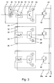
- FIG. 3 shows a first embodiment of the driver circuit arrangement according to the invention.
- FIG. 4 shows a second embodiment of the driver circuit arrangement according to the invention.
- FIG. 1 shows a drive circuit arrangement (10) for a power semiconductor component (40) or a power semiconductor module according to the prior art.
- an input (12) from a higher-level control unit which is connected to a first isolating element (14), preferably a transformer with a transforming action principle, is shown schematically.
- This transformer (14) separates the input signal galvanically from the other circuit parts.
- the secondary side of the transformer (14) is connected to an output stage (22) with associated auxiliary power supply (24), for example + 15V / -15V at 50mA current.
- This output stage (22) controls the associated power semiconductor component (40) or what is to be considered as synonymous below power semiconductor module.
- the monitoring and diagnostic functionality (20) which includes, for example, VCE monitoring, temperature monitoring, and auxiliary voltage monitoring in the prior art.
- FIG. 2 shows a circuit arrangement comprising a superordinate control (50) with a plurality of control lines (52) to individual driver circuit arrangements (10).
- Each of these individual driver circuit arrangements (10) is designed in accordance with the example according to FIG. 1.
- optical waveguides can also be used as the control line (52) in such a controller.
- Such a solution according to the prior art is scalable by increasing the number of control lines (52) and also by assigning the number of individual driver circuit arrangements (10) Power semiconductor modules (40) is increased. Also known is the serial connection instead of the illustrated parallel.
- FIG. 3 shows a first embodiment of the driver circuit arrangement according to the invention. Shown is a master-slave configuration, wherein the master (10) has all the functional groups of the driver circuit arrangement shown in FIG.
- the master has at least one further isolating element (18), wherein this further isolating element (18) is connected between the first isolating element (14) and the output stage (22).
- the slaves (30) in turn have no input from a higher-level drive with associated transformer, but only an isolator (34) connected to an output stage (22) with associated auxiliary voltage supply (24) for controlling at least one associated power semiconductor device (40). It may be preferable to additionally design the slave (30) with limited monitoring functionality.
- the transformer (14) of the master (10) is connected to a further isolating element (18), here an optocoupler whose output (28) is connected to an input (32) of the optocoupler (34) of the first slave (30 ) connected is. Furthermore, the secondary side of the optocoupler (18) is connected to the output stage (22).
- This additional optocoupler (18) thus does not change the functionality compared with a single driver circuit arrangement according to FIG. 1.
- the optocoupler (18) increases the interference immunity of the master (10) since it provides a galvanic connection between a defective power semiconductor component (40) and the Control unit prevented even in case of error.
- Each slave (30) of the scalable driver circuitry has an input (32) connected to a downstream isolator (34), also an optocoupler, and an output (36) connected to its output.
- the secondary side of the optocoupler (34) is connected to an output stage (22) with auxiliary voltage supply (24) for driving the associated power semiconductor component (40).
- the optocoupler (34) of the first slave (30) is connected to the output (28) of the optocoupler (18) of the master (10) and each further slave (30) is connected to its input (32) of the optocoupler (30). 34) connected to the output (36) of the optocoupler (34) of the upstream slave.
- the output of the Optocoupler (34) of the series last slaves (30) of the serial circuit is connected to the emitter (42) of the associated power semiconductor device (40). Since it is a scalable arrangement, the power semiconductor components (40) or the power semiconductor modules are connected in parallel with one another, wherein the collectors and the emitter each have a common connection (44, 46).
- the serial master-slave circuit has the advantage that when using identical optocouplers (18, 34) due to approximately the same, almost identical, time delay, both the master (10) and all slaves (30) at the same time the associated power semiconductor devices (40). turn on. Furthermore, the serial connection of the optocouplers (18, 34) can serve as a failure detection of a slave (30).
- FIG. 4 shows a second embodiment of the driver circuit arrangement according to the invention.
- the arrangement of the power semiconductor components (40) or power semiconductor modules is identical to that of Fig. 3.
- the functionalities of the master (10) and the slaves (30) is also identical to those of Fig. 3.
- the master-slave arrangement is parallel here connected.
- the transmitter (14) has a plurality of outputs (16 a / b / c) with which both the optocoupler (18) of the master (10) and those (34) of the slaves (30) are connected on an equal basis.
- the outputs of all optocouplers (18, 34) are each connected to the emitter (42) of the associated power semiconductor components (40).
- the serial configuration of the master-slave circuit has the advantage that in the case of redundant systems with a larger number of power semiconductor components (40) than would be required according to the required power, the function of the entire system is completely retained if one power semiconductor component fails.
- the optocouplers (18, 34) and the galvanic separation achieved thereby a retroactive effect of the failure of one component on other components is reliably prevented.
Landscapes
- Engineering & Computer Science (AREA)
- Power Engineering (AREA)
- Electronic Switches (AREA)
- Power Conversion In General (AREA)
- Logic Circuits (AREA)
Applications Claiming Priority (1)
| Application Number | Priority Date | Filing Date | Title |
|---|---|---|---|
| DE102005052800A DE102005052800A1 (de) | 2005-11-05 | 2005-11-05 | Treiberschaltungsanordnung zur Ansteuerung von leistungselektronischen Schaltungen |
Publications (2)
| Publication Number | Publication Date |
|---|---|
| EP1783885A2 true EP1783885A2 (fr) | 2007-05-09 |
| EP1783885A3 EP1783885A3 (fr) | 2009-04-29 |
Family
ID=37835392
Family Applications (1)
| Application Number | Title | Priority Date | Filing Date |
|---|---|---|---|
| EP06022572A Withdrawn EP1783885A3 (fr) | 2005-11-05 | 2006-10-28 | Circuit d'agencement pour commander des circuits électroniques de puissance |
Country Status (2)
| Country | Link |
|---|---|
| EP (1) | EP1783885A3 (fr) |
| DE (1) | DE102005052800A1 (fr) |
Cited By (3)
| Publication number | Priority date | Publication date | Assignee | Title |
|---|---|---|---|---|
| DE102007029349A1 (de) * | 2007-06-26 | 2008-08-28 | Siemens Ag | Anordnung zur sicheren elektrischen Trennung von Schaltungsteilen |
| DE102007031140A1 (de) * | 2007-07-02 | 2009-01-08 | Siemens Ag | Vorrichtung zum Umrichten eines elektrischen Stromes |
| WO2018138017A1 (fr) * | 2017-01-25 | 2018-08-02 | Siemens Aktiengesellschaft | Module à semi-conducteur |
Family Cites Families (5)
| Publication number | Priority date | Publication date | Assignee | Title |
|---|---|---|---|---|
| JPS57135671A (en) * | 1981-02-13 | 1982-08-21 | Toshiba Corp | Gate circuit for thyristor converter |
| US5227781A (en) * | 1991-03-01 | 1993-07-13 | Litton Systems, Inc. | Mosfet switch matrix |
| DE10205832A1 (de) * | 2002-02-13 | 2003-08-28 | Semikron Elektronik Gmbh | Ansteuerung für Stromrichterventile |
| TW588499B (en) * | 2002-12-30 | 2004-05-21 | Ind Tech Res Inst | Programmable photocoupler-isolated wide band modulator fore high voltage power supply |
| US6882212B2 (en) * | 2003-05-16 | 2005-04-19 | Power Integrations, Inc. | Method and apparatus for extending the size of a transistor beyond one integrated circuit |
-
2005
- 2005-11-05 DE DE102005052800A patent/DE102005052800A1/de not_active Withdrawn
-
2006
- 2006-10-28 EP EP06022572A patent/EP1783885A3/fr not_active Withdrawn
Cited By (4)
| Publication number | Priority date | Publication date | Assignee | Title |
|---|---|---|---|---|
| DE102007029349A1 (de) * | 2007-06-26 | 2008-08-28 | Siemens Ag | Anordnung zur sicheren elektrischen Trennung von Schaltungsteilen |
| DE102007031140A1 (de) * | 2007-07-02 | 2009-01-08 | Siemens Ag | Vorrichtung zum Umrichten eines elektrischen Stromes |
| WO2009003834A3 (fr) * | 2007-07-02 | 2009-03-19 | Siemens Ag | Dispositif de conversion de courant électrique |
| WO2018138017A1 (fr) * | 2017-01-25 | 2018-08-02 | Siemens Aktiengesellschaft | Module à semi-conducteur |
Also Published As
| Publication number | Publication date |
|---|---|
| EP1783885A3 (fr) | 2009-04-29 |
| DE102005052800A1 (de) | 2007-08-16 |
Similar Documents
| Publication | Publication Date | Title |
|---|---|---|
| EP1965482B1 (fr) | Réseau ASI pour des zones en danger d'explosion | |
| EP3381116B1 (fr) | Onduleur multiniveaux modulaire | |
| EP1950096B1 (fr) | Système modulaire | |
| EP1873915B1 (fr) | Circuit d'entrée sécurisé doté d'un raccordement périphérique sur un canal unique pour l'entrée d'un utilisateur de bus | |
| EP1873916A2 (fr) | Circuit de sortie sécurisé doté d'un raccordement périphérique sur un seul canal pour la sortie d'un utilisateur de bus | |
| DE102016220197A1 (de) | Verfahren zum Verarbeiten von Daten für ein automatisiertes Fahrzeug | |
| DE102014213206B4 (de) | Steueranordnung für sicherheitsrelevante Aktoren | |
| EP3562283A1 (fr) | Arrangement modulaire backplane | |
| CH618029A5 (fr) | ||
| DE212012000249U1 (de) | Vorrichtung zum eigensicheren Versorgen, Ansteuern und/oder Auswerten von Feldgeräten im explosionsgeschützten Bereich | |
| EP2511984B1 (fr) | Agencement de commande d'une installation | |
| DE102005052800A1 (de) | Treiberschaltungsanordnung zur Ansteuerung von leistungselektronischen Schaltungen | |
| EP1695158B1 (fr) | Dispositif de transmission de donnees a securite intrinseque | |
| DE19947501A1 (de) | Aktuator-Sensor-Interface-Slave | |
| DE102019203517A1 (de) | Verfahren zur Energieversorgung von Verbrauchern eines Bordnetzes für ein Fahrzeug, sowie ein Bordnetz für ein Fahrzeug | |
| DE102019003206B3 (de) | Sicherheitsanordnung | |
| EP0093899B1 (fr) | Circuit pour l'adaptation d'un dispositif d'essai à un objet à l'essai | |
| DE19813952C1 (de) | Signalisierungsendstufe zur Erzeugung digitaler Spannungssignale auf einem Bussystem | |
| EP0292817A2 (fr) | Circuit pour l'obtention de signaux numériques bipolaires | |
| DE102020115210A1 (de) | Steuersystem für ein mindestens zwei Übertragungsleitungen aufweisendes Bussystem | |
| DE102019125293A1 (de) | Gleichspannungswandlung in einem Bordnetz | |
| EP4114157B1 (fr) | Agencement pour un système redondant de commande | |
| EP1950399A1 (fr) | Système doté de déviations dýutilisateurs | |
| EP3665873B1 (fr) | Transmission de signaux | |
| WO2009065437A1 (fr) | Système de deux dispositifs galvaniquement séparés communiquant bidirectionnellement entre eux |
Legal Events
| Date | Code | Title | Description |
|---|---|---|---|
| PUAI | Public reference made under article 153(3) epc to a published international application that has entered the european phase |
Free format text: ORIGINAL CODE: 0009012 |
|
| AK | Designated contracting states |
Kind code of ref document: A2 Designated state(s): AT BE BG CH CY CZ DE DK EE ES FI FR GB GR HU IE IS IT LI LT LU LV MC NL PL PT RO SE SI SK TR |
|
| AX | Request for extension of the european patent |
Extension state: AL BA HR MK YU |
|
| PUAL | Search report despatched |
Free format text: ORIGINAL CODE: 0009013 |
|
| AK | Designated contracting states |
Kind code of ref document: A3 Designated state(s): AT BE BG CH CY CZ DE DK EE ES FI FR GB GR HU IE IS IT LI LT LU LV MC NL PL PT RO SE SI SK TR |
|
| AX | Request for extension of the european patent |
Extension state: AL BA HR MK RS |
|
| 17P | Request for examination filed |
Effective date: 20090427 |
|
| 17Q | First examination report despatched |
Effective date: 20090624 |
|
| AKX | Designation fees paid |
Designated state(s): AT BE BG CH CY CZ DE DK EE ES FI FR GB GR HU IE IS IT LI LT LU LV MC NL PL PT RO SE SI SK TR |
|
| STAA | Information on the status of an ep patent application or granted ep patent |
Free format text: STATUS: THE APPLICATION IS DEEMED TO BE WITHDRAWN |
|
| 18D | Application deemed to be withdrawn |
Effective date: 20150428 |