EP1784055A2 - Système d' éclairage - Google Patents
Système d' éclairage Download PDFInfo
- Publication number
- EP1784055A2 EP1784055A2 EP06021358A EP06021358A EP1784055A2 EP 1784055 A2 EP1784055 A2 EP 1784055A2 EP 06021358 A EP06021358 A EP 06021358A EP 06021358 A EP06021358 A EP 06021358A EP 1784055 A2 EP1784055 A2 EP 1784055A2
- Authority
- EP
- European Patent Office
- Prior art keywords
- light emitting
- emitting element
- light
- lighting system
- emission
- Prior art date
- Legal status (The legal status is an assumption and is not a legal conclusion. Google has not performed a legal analysis and makes no representation as to the accuracy of the status listed.)
- Withdrawn
Links
Images




Classifications
-
- G—PHYSICS
- G09—EDUCATION; CRYPTOGRAPHY; DISPLAY; ADVERTISING; SEALS
- G09G—ARRANGEMENTS OR CIRCUITS FOR CONTROL OF INDICATING DEVICES USING STATIC MEANS TO PRESENT VARIABLE INFORMATION
- G09G3/00—Control arrangements or circuits, of interest only in connection with visual indicators other than cathode-ray tubes
- G09G3/20—Control arrangements or circuits, of interest only in connection with visual indicators other than cathode-ray tubes for presentation of an assembly of a number of characters, e.g. a page, by composing the assembly by combination of individual elements arranged in a matrix no fixed position being assigned to or needed to be assigned to the individual characters or partial characters
- G09G3/22—Control arrangements or circuits, of interest only in connection with visual indicators other than cathode-ray tubes for presentation of an assembly of a number of characters, e.g. a page, by composing the assembly by combination of individual elements arranged in a matrix no fixed position being assigned to or needed to be assigned to the individual characters or partial characters using controlled light sources
- G09G3/30—Control arrangements or circuits, of interest only in connection with visual indicators other than cathode-ray tubes for presentation of an assembly of a number of characters, e.g. a page, by composing the assembly by combination of individual elements arranged in a matrix no fixed position being assigned to or needed to be assigned to the individual characters or partial characters using controlled light sources using electroluminescent panels
- G09G3/32—Control arrangements or circuits, of interest only in connection with visual indicators other than cathode-ray tubes for presentation of an assembly of a number of characters, e.g. a page, by composing the assembly by combination of individual elements arranged in a matrix no fixed position being assigned to or needed to be assigned to the individual characters or partial characters using controlled light sources using electroluminescent panels semiconductive, e.g. using light-emitting diodes [LED]
- G09G3/3208—Control arrangements or circuits, of interest only in connection with visual indicators other than cathode-ray tubes for presentation of an assembly of a number of characters, e.g. a page, by composing the assembly by combination of individual elements arranged in a matrix no fixed position being assigned to or needed to be assigned to the individual characters or partial characters using controlled light sources using electroluminescent panels semiconductive, e.g. using light-emitting diodes [LED] organic, e.g. using organic light-emitting diodes [OLED]
-
- H—ELECTRICITY
- H05—ELECTRIC TECHNIQUES NOT OTHERWISE PROVIDED FOR
- H05B—ELECTRIC HEATING; ELECTRIC LIGHT SOURCES NOT OTHERWISE PROVIDED FOR; CIRCUIT ARRANGEMENTS FOR ELECTRIC LIGHT SOURCES, IN GENERAL
- H05B45/00—Circuit arrangements for operating light-emitting diodes [LED]
- H05B45/60—Circuit arrangements for operating LEDs comprising organic material, e.g. for operating organic light-emitting diodes [OLED] or polymer light-emitting diodes [PLED]
-
- H—ELECTRICITY
- H10—SEMICONDUCTOR DEVICES; ELECTRIC SOLID-STATE DEVICES NOT OTHERWISE PROVIDED FOR
- H10K—ORGANIC ELECTRIC SOLID-STATE DEVICES
- H10K50/00—Organic light-emitting devices
- H10K50/10—OLEDs or polymer light-emitting diodes [PLED]
- H10K50/11—OLEDs or polymer light-emitting diodes [PLED] characterised by the electroluminescent [EL] layers
- H10K50/125—OLEDs or polymer light-emitting diodes [PLED] characterised by the electroluminescent [EL] layers specially adapted for multicolour light emission, e.g. for emitting white light
-
- G—PHYSICS
- G09—EDUCATION; CRYPTOGRAPHY; DISPLAY; ADVERTISING; SEALS
- G09G—ARRANGEMENTS OR CIRCUITS FOR CONTROL OF INDICATING DEVICES USING STATIC MEANS TO PRESENT VARIABLE INFORMATION
- G09G2320/00—Control of display operating conditions
- G09G2320/04—Maintaining the quality of display appearance
- G09G2320/043—Preventing or counteracting the effects of ageing
- G09G2320/048—Preventing or counteracting the effects of ageing using evaluation of the usage time
-
- G—PHYSICS
- G09—EDUCATION; CRYPTOGRAPHY; DISPLAY; ADVERTISING; SEALS
- G09G—ARRANGEMENTS OR CIRCUITS FOR CONTROL OF INDICATING DEVICES USING STATIC MEANS TO PRESENT VARIABLE INFORMATION
- G09G2320/00—Control of display operating conditions
- G09G2320/06—Adjustment of display parameters
- G09G2320/0666—Adjustment of display parameters for control of colour parameters, e.g. colour temperature
-
- G—PHYSICS
- G09—EDUCATION; CRYPTOGRAPHY; DISPLAY; ADVERTISING; SEALS
- G09G—ARRANGEMENTS OR CIRCUITS FOR CONTROL OF INDICATING DEVICES USING STATIC MEANS TO PRESENT VARIABLE INFORMATION
- G09G3/00—Control arrangements or circuits, of interest only in connection with visual indicators other than cathode-ray tubes
- G09G3/20—Control arrangements or circuits, of interest only in connection with visual indicators other than cathode-ray tubes for presentation of an assembly of a number of characters, e.g. a page, by composing the assembly by combination of individual elements arranged in a matrix no fixed position being assigned to or needed to be assigned to the individual characters or partial characters
- G09G3/22—Control arrangements or circuits, of interest only in connection with visual indicators other than cathode-ray tubes for presentation of an assembly of a number of characters, e.g. a page, by composing the assembly by combination of individual elements arranged in a matrix no fixed position being assigned to or needed to be assigned to the individual characters or partial characters using controlled light sources
- G09G3/30—Control arrangements or circuits, of interest only in connection with visual indicators other than cathode-ray tubes for presentation of an assembly of a number of characters, e.g. a page, by composing the assembly by combination of individual elements arranged in a matrix no fixed position being assigned to or needed to be assigned to the individual characters or partial characters using controlled light sources using electroluminescent panels
- G09G3/32—Control arrangements or circuits, of interest only in connection with visual indicators other than cathode-ray tubes for presentation of an assembly of a number of characters, e.g. a page, by composing the assembly by combination of individual elements arranged in a matrix no fixed position being assigned to or needed to be assigned to the individual characters or partial characters using controlled light sources using electroluminescent panels semiconductive, e.g. using light-emitting diodes [LED]
- G09G3/3208—Control arrangements or circuits, of interest only in connection with visual indicators other than cathode-ray tubes for presentation of an assembly of a number of characters, e.g. a page, by composing the assembly by combination of individual elements arranged in a matrix no fixed position being assigned to or needed to be assigned to the individual characters or partial characters using controlled light sources using electroluminescent panels semiconductive, e.g. using light-emitting diodes [LED] organic, e.g. using organic light-emitting diodes [OLED]
- G09G3/3216—Control arrangements or circuits, of interest only in connection with visual indicators other than cathode-ray tubes for presentation of an assembly of a number of characters, e.g. a page, by composing the assembly by combination of individual elements arranged in a matrix no fixed position being assigned to or needed to be assigned to the individual characters or partial characters using controlled light sources using electroluminescent panels semiconductive, e.g. using light-emitting diodes [LED] organic, e.g. using organic light-emitting diodes [OLED] using a passive matrix
-
- G—PHYSICS
- G09—EDUCATION; CRYPTOGRAPHY; DISPLAY; ADVERTISING; SEALS
- G09G—ARRANGEMENTS OR CIRCUITS FOR CONTROL OF INDICATING DEVICES USING STATIC MEANS TO PRESENT VARIABLE INFORMATION
- G09G3/00—Control arrangements or circuits, of interest only in connection with visual indicators other than cathode-ray tubes
- G09G3/20—Control arrangements or circuits, of interest only in connection with visual indicators other than cathode-ray tubes for presentation of an assembly of a number of characters, e.g. a page, by composing the assembly by combination of individual elements arranged in a matrix no fixed position being assigned to or needed to be assigned to the individual characters or partial characters
- G09G3/22—Control arrangements or circuits, of interest only in connection with visual indicators other than cathode-ray tubes for presentation of an assembly of a number of characters, e.g. a page, by composing the assembly by combination of individual elements arranged in a matrix no fixed position being assigned to or needed to be assigned to the individual characters or partial characters using controlled light sources
- G09G3/30—Control arrangements or circuits, of interest only in connection with visual indicators other than cathode-ray tubes for presentation of an assembly of a number of characters, e.g. a page, by composing the assembly by combination of individual elements arranged in a matrix no fixed position being assigned to or needed to be assigned to the individual characters or partial characters using controlled light sources using electroluminescent panels
- G09G3/32—Control arrangements or circuits, of interest only in connection with visual indicators other than cathode-ray tubes for presentation of an assembly of a number of characters, e.g. a page, by composing the assembly by combination of individual elements arranged in a matrix no fixed position being assigned to or needed to be assigned to the individual characters or partial characters using controlled light sources using electroluminescent panels semiconductive, e.g. using light-emitting diodes [LED]
- G09G3/3208—Control arrangements or circuits, of interest only in connection with visual indicators other than cathode-ray tubes for presentation of an assembly of a number of characters, e.g. a page, by composing the assembly by combination of individual elements arranged in a matrix no fixed position being assigned to or needed to be assigned to the individual characters or partial characters using controlled light sources using electroluminescent panels semiconductive, e.g. using light-emitting diodes [LED] organic, e.g. using organic light-emitting diodes [OLED]
- G09G3/3225—Control arrangements or circuits, of interest only in connection with visual indicators other than cathode-ray tubes for presentation of an assembly of a number of characters, e.g. a page, by composing the assembly by combination of individual elements arranged in a matrix no fixed position being assigned to or needed to be assigned to the individual characters or partial characters using controlled light sources using electroluminescent panels semiconductive, e.g. using light-emitting diodes [LED] organic, e.g. using organic light-emitting diodes [OLED] using an active matrix
-
- H—ELECTRICITY
- H10—SEMICONDUCTOR DEVICES; ELECTRIC SOLID-STATE DEVICES NOT OTHERWISE PROVIDED FOR
- H10K—ORGANIC ELECTRIC SOLID-STATE DEVICES
- H10K50/00—Organic light-emitting devices
- H10K50/10—OLEDs or polymer light-emitting diodes [PLED]
- H10K50/19—Tandem OLEDs
-
- H—ELECTRICITY
- H10—SEMICONDUCTOR DEVICES; ELECTRIC SOLID-STATE DEVICES NOT OTHERWISE PROVIDED FOR
- H10K—ORGANIC ELECTRIC SOLID-STATE DEVICES
- H10K59/00—Integrated devices, or assemblies of multiple devices, comprising at least one organic light-emitting element covered by group H10K50/00
- H10K59/10—OLED displays
- H10K59/12—Active-matrix OLED [AMOLED] displays
-
- H—ELECTRICITY
- H10—SEMICONDUCTOR DEVICES; ELECTRIC SOLID-STATE DEVICES NOT OTHERWISE PROVIDED FOR
- H10K—ORGANIC ELECTRIC SOLID-STATE DEVICES
- H10K59/00—Integrated devices, or assemblies of multiple devices, comprising at least one organic light-emitting element covered by group H10K50/00
- H10K59/30—Devices specially adapted for multicolour light emission
- H10K59/35—Devices specially adapted for multicolour light emission comprising red-green-blue [RGB] subpixels
-
- Y—GENERAL TAGGING OF NEW TECHNOLOGICAL DEVELOPMENTS; GENERAL TAGGING OF CROSS-SECTIONAL TECHNOLOGIES SPANNING OVER SEVERAL SECTIONS OF THE IPC; TECHNICAL SUBJECTS COVERED BY FORMER USPC CROSS-REFERENCE ART COLLECTIONS [XRACs] AND DIGESTS
- Y02—TECHNOLOGIES OR APPLICATIONS FOR MITIGATION OR ADAPTATION AGAINST CLIMATE CHANGE
- Y02B—CLIMATE CHANGE MITIGATION TECHNOLOGIES RELATED TO BUILDINGS, e.g. HOUSING, HOUSE APPLIANCES OR RELATED END-USER APPLICATIONS
- Y02B20/00—Energy efficient lighting technologies, e.g. halogen lamps or gas discharge lamps
- Y02B20/30—Semiconductor lamps, e.g. solid state lamps [SSL] light emitting diodes [LED] or organic LED [OLED]
Definitions
- the present invention relates to a light emitting device which uses a light emitting element utilizing electroluminescence, and particularly, a lighting system.
- a light emitting element is a self-light emitting element and attempted to be used as a lighting system.
- the lighting system using the light emitting element can provide lighting systems tailored to customers' needs such as high efficiency and excellent color rendering properties.
- a light emitting mechanism of the light emitting element emits light by applying a voltage between a pair of electrodes where a light emitting layer is interposed, so that electrons injected from a cathode and holes injected from an anode are recombined with each other at a light emitting center of the light emitting layer to form molecular excitons and the molecular excitons release energy when returning to a ground state.
- Singlet excitation and triplet excitation are known as excited states, and light emission can be achieved through either of the excited states.
- a light emitting element having a structure in which a plurality of light emitting units divided by charge generation layers are stacked between an anode and a cathode opposing to each other has been reported to achieve longer life when emitting light with high luminance (refer to Reference 1: Japanese Patent Laid-Open No. 2003-45676 and Reference 2: Toshio Matsumoto, Takeshi Nakada, Jun Endo, Koichi Mori, Norihumi Kawamura, Akira Tokoi, Junji Kido, IDW '03, 1285-1288 ).
- This charge generation layer needs to be formed of a material having a function to inject carriers and having an excellent light transmitting property.
- a light emitting element provided with a plurality of light emitting units has a problem causing color shift where an emission color of the light emitting element changes as time passes unless light emitting units to be combined with each other have the same length of life.
- the color shift is a phenomenon in which a proportion of luminance of each light emitting unit is changed and an emission color as the light emitting element is changed.
- constant luminance can be maintained by increasing a voltage to be applied, but color shift cannot be solved only by adjusting a voltage to be applied. For example, when the life of a blue light emitting material is shorter in FIG 8A, an emission color gradually becomes yellowish white as shown in FIG 8C after a certain period of time with the light emitting element lighted.
- One feature of the present invention is a lighting system including a light emitting region divided into a plurality of regions, each of the divided light emitting regions being provided with a plurality of light emitting elements, at least one of the plurality of light emitting elements being a first light emitting element including a plurality of light emitting units, at least one of the plurality of light emitting elements being a second light emitting element, the second light emitting element emitting light of a complementary color of a second emission color when an initial emission color of the first light emitting element is referred to as a first emission color and an emission color of the first light emitting element after change over time is referred to as the second emission color; and a control means which controls light emission of the first light emitting element and that of the second light emitting element independently.
- light emission of the first light emitting element and that of the second light emitting element can be controlled independently even in the case where the emission color of the first light emitting element changes from the first emission color to the second emission color as time passes.
- the second emission color and an emission color of the second light emitting element are in a relation of complementary colors, a change in emission color of a light emitting region as a whole can be suppressed.
- Another feature of the present invention is a lighting system including a light emitting region divided into a plurality of regions, each of the divided light emitting regions being provided with a plurality of light emitting elements, at least one of the plurality of light emitting elements being a first light emitting element including a plurality of light emitting units, at least of the plurality of light emitting elements being a second light emitting element, the second light emitting element including a light emitting unit formed of the same material as that of a light emitting unit having a short life among the plurality of light emitting units of the first light emitting element; and a control means which controls light emission of the first light emitting element and that of the second light emitting element independently.
- the first light emitting element and the second light emitting element can be controlled independently even in the case where the emission color of the first light emitting element changes as time passes. Since the first light emitting element and the second light emitting element including a light emitting unit formed of the same material as that of a light emitting unit having a short life among the light emitting units included in the first light emitting element, are in the same divided light emitting region, a change in emission color of the light emitting region as a whole can be suppressed by controlling the light emission of the first light emitting element and that of the second light emitting element.
- Another feature of the present invention is a lighting system including a light emitting region divided into a plurality of regions, each of the divided light emitting regions including a first light emitting element and a second light emitting element, the first light emitting element including a plurality of light emitting units, the second light emitting element including a light emitting unit formed of the same material as that of a light emitting unit having a short life among the plurality of light emitting units included in the first light emitting element; and a control means which controls light emission of the first light emitting element and that of the second light emitting element independently.
- the first light emitting element and the second light emitting element can be controlled independently even in the case where the emission color of the first light emitting element changes as time passes. Since the first light emitting element and the second light emitting element including a light emitting unit formed of the same material as that of a light emitting unit having a short life among the light emitting units included in the first light emitting element, are in the same divided light emitting region, a change in emission color of the light emitting region as a whole can be suppressed by controlling the light emission of the first light emitting element and that of the second light emitting element.
- Another feature of the present invention is a lighting system including a light emitting region divided into a plurality of regions, each of the divided light emitting regions including a first light emitting element provided with a plurality of light emitting units and a second light emitting element, an initial emission color of the first light emitting element being white, the second light emitting element emitting light of a complementary color of a second emission color when an emission color of the first light emitting element after change over time is referred to as the second emission color; and a control means which controls light emission of the second light emitting element with a change in emission color of the first light emitting element.
- Another feature of the present invention is a lighting system including a light emitting region divided into a plurality of regions, each of the divided light emitting regions including a first light emitting element provided with a plurality of light emitting units and a second light emitting element, the first light emitting element emitting white light, the second light emitting element emitting light of the same color as that of a light emitting material having a short life among light emitting materials contained in the first light emitting element; and a control means which controls light emission of the second light emitting element with a change in emission color of the first light emitting element.
- a lighting system including a light emitting region divided into a plurality of regions, each of the divided light emitting region including a first light emitting element provided with a plurality of light emitting units and a second light emitting element; and a control means which suppresses changes in luminance of the divided light emitting region as a whole by intensifying a luminance of the second light emitting element in accordance with a change in luminance of the first light emitting element from a first luminance to a second luminance when an initial luminance of the first light emitting element is referred to as the first luminance and a luminance of the first light emitting element after change over time is referred to as the second luminance.
- Another feature of the present invention is a lighting system including a light emitting region and a monitor element, wherein the light emitting region is divided into a plurality of regions, each of the divided light emitting regions includes a first light emitting element provided with a plurality of light emitting units and a second light emitting element, and a control means which adjusts a luminance of the second light emitting element after t hours so as to satisfy Formula (1) when a luminance of the first light emitting element as a start of light emission is denoted by L total (0), a luminance of the first light emitting element after t hours by L tolal (t), an amount of change in luminance of the monitor element between at the start of light emission and after t hours by ⁇ L mon , and the luminance of the second light emitting element after t hours by ⁇ L 2 .
- ⁇ L 2 L total 0 - L total t - ⁇ ⁇ ⁇ L mon ( ⁇ is a factor with respect to luminance of the monitor element.)
- the second light emitting element may be either a light emitting element including one light emitting unit or a light emitting element provided with a plurality of light emitting units.
- the plurality of light emitting regions may be formed in matrix or in stripes.
- the lighting system of the present invention can emit light with high luminance because it has a stacked structure in which a plurality of light emitting units is stacked.
- the lighting system of the present invention causes little change in emission color even after being used for a long time and has a long life.
- This embodiment mode explains one mode of a lighting system of the present invention.
- a light emitting region is divided into a plurality of regions, and each of the divided light emitting regions includes a plurality of light emitting elements.
- One is a stacked light emitting element in which a plurality of light emitting units is stacked, and another is a correction light emitting element.
- the stacked light emitting element is referred to as a first light emitting element, and the correction light emitting element is referred to as a second light emitting element.
- the first light emitting element is formed by stacking a plurality of light emitting units so as to provide a desired emission color as a whole.
- the first light emitting element is formed so that an initial emission color is a desired first emission color.
- a stacked light emitting element which emits white light can be obtained by stacking light emitting units which emit light of complementary colors.
- the second light emitting element is a light emitting element which emits light of a complimentary color of an emission color (second emission color) after the first light emitting element is deteriorated.
- the first light emitting element is formed by stacking two light emitting units so as to provide white light emission
- a light emitting material used for a light emitting unit with a shorter life of the two light emitting units included in the first light emitting element can be used for the second light emitting element.
- the lighting system of the present invention can provide light emission of the desired first emission color only by light emission of the first light emitting element.
- the first light emitting element that is the stacked light emitting element deterioration occurs, an emission color changes, and luminance also changes as emission time passes.
- the emission color of the first light emitting element changes from the first emission color to the second emission color.
- the luminance of the first light emitting element also changes from a first luminance to a second luminance. This is caused by a difference in deterioration with time of materials contained in the light emitting units.
- the emission color of the first light emitting element is changed and luminance is decreased with time
- light emission of the second light emitting element is intensified by a second control means to suppress changes in emission color and luminance of the divided light emitting region.
- light emission is controlled using a first control means which controls light emission of the first light emitting element and the second control means which controls light emission of the second light emitting element so that an emission color of one divided light emitting region does not change. Therefore, a change in emission color of the light emitting region as a whole can be suppressed. In addition, a change in luminance of the divided light emitting region as a whole can be suppressed.
- the first light emitting element and the second light emitting element are preferably provided adjacent to each other. By providing the first light emitting element and the second light emitting element adjacent to each other, a difference between an emission color of the first light emitting element and that of the second light emitting element can be made unnoticeable.
- This embodiment mode explains a stacked light emitting element used for a lighting system of the present invention with reference to FIG 5.
- the stacked light emitting element has a structure in which a plurality of light emitting units is stacked with a charge generation layer interposed therebetween.
- FIG. 5 shows a structure in which two light emitting units are stacked as one mode of the stacked light emitting element.
- this embodiment mode explains the case where a first electrode 501 functions as an anode and a second electrode 502 functions as a cathode.
- a substrate 500 is used as a support for the light emitting element.
- the substrate 500 for example, glass, plastic, or the like can be used. Note that another material may alternatively be used as long as it functions as a support in a manufacturing process.
- ITO indium tin oxide
- ZnO zinc oxide
- gold Au
- platinum Pt
- nickel Ni
- tungsten W
- Cr chromium
- Mo molybdenum
- iron Fe
- Co cobalt
- Cu copper
- palladium Pd
- nitride of a metal material for example, titanium nitride (TiN)
- metal, an alloy, a conductive compound, a mixture thereof, or the like having a low work function (specifically, 3.8 eV or lower) is preferably used.
- metal belonging to Group 1 or 2 of the periodic table that is, alkali metal such as lithium (Li) or cesium (Cs); alkaline earth metal such as magnesium (Mg), calcium (Ca), or strontium (Sr); an alloy containing these (MgAg, AlLi, or the like); rare-earth metal such as europium (Eu) or ytterbium (Yb); an alloy containing these; or the like can be used.
- the cathode can also be formed using a material having a high work function, that is, a material generally used for the anode when using an electron injection layer having a high electron injecting property.
- the cathode can be formed of metal such as Al or Ag, or a conductive inorganic compound such as ITO.
- a charge generation layer 521 is a layer serving to inject carriers into a first light emitting unit 511 and a second light emitting unit 512.
- the charge generation layer 521 is preferably formed of a material having a high visible light transmittance, and a transparent conductive film, for example, a film of indium tin oxide (ITO), indium tin oxide containing silicon, indium oxide containing zinc oxide (ZnO) of 2 wt% to 20 wt%, or the like can be used.
- ITO indium tin oxide
- ZnO zinc oxide
- it can be formed to contain not only an inorganic compound but also an organic compound.
- first light emitting unit 511 and the second light emitting unit 512 can be used for various materials, and either a low molecular material or a high molecular material can be used.
- first light emitting unit 511 and the second light emitting unit 512 may be formed to contain not only an organic compound material but also an inorganic compound in part.
- the light emitting unit is formed by appropriately combining a hole injection layer, a hole transport layer, a hole blocking layer, a light emitting layer, an electron transport layer, an electron injection layer, and the like. It may have a single-layer structure or a stacked structure of a plurality of layers.
- the light emitting unit can be formed by various methods such as an evaporation method, an ink-jet method, a spin coating method, or a dip coating method regardless of whether a wet method or a dry method.
- a hole injecting material for forming the hole injection layer various materials can be used. Specifically, metal oxide such as vanadium oxide, molybdenum oxide, ruthenium oxide, or aluminum oxide is preferable. The above oxide may be mixed with an appropriate organic compound. Alternatively, a porphyrin-based compound is effective among organic compounds, and phthalocyanine (abbr.: H 2 Pc), copper phthalocyanine (abbr.: CuPc), or the like can be used.
- H 2 Pc phthalocyanine
- CuPc copper phthalocyanine
- a chemically-doped conductive high molecular compound such as polyethylene dioxythiophene (abbr.: PEDOT) doped with polystyrene sulfonate (abbr.: PSS), or polyaniline (abbr.: PAni).
- PEDOT polyethylene dioxythiophene
- PSS polystyrene sulfonate
- PAni polyaniline
- an aromatic amine-based compound that is, a compound having a benzene ring-nitrogen bond
- a widely-used material is a star-burst aromatic amine compound like N,N' -bis(3-methylphenyl)- N,N' -diphenyl-[1,1'-biphenyl]-4,4'-diamine (hereinafter referred to as TPD), a derivative thereof such as 4,4'-bis[ N -(1-naphthyl)- N -phenyl-amino]-biphenyl (hereinafter referred to as ⁇ -NPD), 4,4',4"-tris( N -carbazolyl)-triphenylamine (hereinafter referred to as TCTA), 4,4',4"-tris( N,N -diphenyl-amino)-triphenylamine (hereinafter referred to as TDATA
- an effective material is specifically various fluorescent materials as well as a metal complex such as tris(8-quinolinolato)aluminum (hereinafter referred to as Alq 3 ), tris(4-methyl-8-quinolinolato)aluminum (hereinafter referred to as Almq 3 ), bis(10-hydroxybenzo[ h ]-quinolinato)beryllium (hereinafter referred to as BeBq 2 ), bis(2-methyl-8-quinolinolato)-(4-hydroxy-biphenylyl)-aluminum (hereinafter referred to as BAlq), bis[2-(2-hydroxyphenyl)-benzoxazolato]zinc (hereinafter referred to as Zn(BOX) 2 ), or bis[2-(2-hydroxyphenyl)-benzothiazolato]zinc (hereinafter referred to as Zn(BTZ) 2 ).
- Alq 3 tris(8-quinolinolato)alumin
- a triplet light emitting material such as bis(2-(2'-benzothienyl)pyridinato- N,C 3' )(acetylacetonato)iridium (abbr.: Ir(btp) 2 (acac)) as well as a singlet light emitting material (fluorescent material) such as 4-(dicyanomethylene)-2-methyl-6-( p -dimethylaminostyryl)-4 H -pyran (abbr.: DCM1), 4-(dicyanomethylene)-2-methyl-6-(julolidine-4-yl-vinyl)-4 H -pyran (abbr.: DCM2), N,N' -dimethylquinacridon (abbr.: DMQd), 9,10-diphenylanthracene, 5,12-diphenyltetracene (abbr.: DPT),
- a triplet light emitting material such as bis(2-(2'-benzothienyl)
- a metal complex such as above-mentioned Alq 3 , tris(4-methyl-8-quinolinolato)aluminum (abbr.: Almq 3 ), bis(2-methyl-8-quinolinolato)-4-phenylphenolato-aluminum (abbr.: BAlq), tris(8-quinolinolato)gallium (abbr.: Gaq 3 ), bis(2-methyl-8-quinolinolato)-4-phenylphenolato-gallium (abbr.: BGaq), bis(10-hydroxybenzo[ h ]-quinolinato)beryllium (abbr.: BeBq 2 ), bis[2-(2-hydroxyphenyl)benzoxazolato]zinc (abbr.: Zn(BOX) 2 ), or bis[2-(2-hydroxyphenyl)benzothiazolato]zinc (abbr.: Zn(BTZ) 2
- 2-(4-biphenylyl)-5-(4- tert -butylphenyl)-1,3,4-oxadiazole (abbr.: PBD), 1,3-bis[5-( p - tert -butylphenyl)-1,3,4-oxadiazole-2-yl]benzene (abbr.: OXD-7), 3-(4- tert -butylphenyl)-4-phenyl-5-(4-biphenylyl)-1,2,4-triazole (abbr.: TAZ), 3-(4- tert -butylphenyl)-4-(4-ethylphenyl)-5-(4-biphenylyl)-1,2,4-triazole (abbr.: p -EtTAZ), bathophenanthroline (abbr.: BPhen), bathocuproin (abbr.: BCP), or the like can be used.
- PBD 1,3-bis[
- an electron injecting material which can be used for the electron injection layer
- the above-described electron transporting material can be used.
- an ultrathin film of an insulator for example, alkali metal halide such as LiF or CsF, alkaline earth halide such as CsF 2 , or alkali metal oxide such as Li 2 O is commonly used.
- an alkali metal complex such as lithium acetylacetonate (abbr.: Li(acac)) or 8-quinolinolato-lithium (abbr.: Liq) is also effective.
- a layer in which the above-described electron transporting material and metal having a low work function such as Mg, Li, or Cs are combined with each other can be used as the electron injection layer.
- metal oxide such as molybdenum oxide (MoO x ), vanadium oxide (VO x ), ruthenium oxide (RuO x ), or tungsten oxide (WO x ) or a benzoxazole derivative, and one or more of alkali metal, alkaline earth metal, or transition metal may be contained.
- titanium oxide may be used.
- FIG 5 shows the structure in which two light emitting units are provided, but the present invention is not limited thereto. Three or more light emitting units may be provided. In addition, light emitting units to be stacked do not need to have the same structure, and light emitting units formed of different materials may be stacked.
- a light emitting unit including a single light emitting unit can also be formed using the above-described materials appropriately.
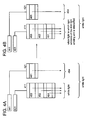
- This embodiment mode explains a lighting system which uses a stacked light emitting element including two light emitting units as a first light emitting element and a light emitting element including one light emitting unit as a second light emitting element, with reference to FIGS. 1A and 1B.
- this embodiment mode explains the case where a divided light emitting region emits white light, the present invention can be applied to a case other than the case of white light emission.
- a first light emitting element 111 is a stacked light emitting element including two light emitting units.
- a first light emitting unit 151 and a second light emitting unit 152 contain different light emitting materials and emit light of different colors. For example, white light emission can be achieved by forming the first light emitting unit 151 to emit blue light and the second light emitting unit 152 to emit orange light and optimizing thickness by optical design.
- a second light emitting element 121 includes one light emitting unit 161 and contains a light emitting material which is contained in the first light emitting element and contained in the first light emitting unit 151 having a shorter life than that of the second light emitting unit 152.
- the first light emitting element 111 is formed to emit white light at the start of light emission
- the second light emitting element 121 is formed to emit light of the same color 162 as that of the first light emitting unit.
- the lighting system described in this embodiment mode realizes aimed white light emission only by light emission of the first light emitting element 111 at the start of light emission (FIG 1A). However, an emission color and luminance of the first light emitting element are changed as time passes.
- the emission color of the first light emitting element 111 becomes close to an emission color of the light emitting material contained in the second light emitting unit.
- the emission color of the first light emitting element changes from a first emission color at the start of light emission to a second emission color.
- the luminance of the first light emitting element also changes from a first luminance at the start of light emission to a second luminance.
- light emission of the second light emitting element 121 is intensified in accordance with changes in emission color and luminance of the first light emitting element 111.
- the light emission of the second light emitting element 121 which provides a complementary color of the second emission color, that is, the same emission color as that of the first light emitting unit is intensified, and the intensity of light emission is adjusted so as to maintain the emission color of one divided light emitting region to white (FIG 1B).
- Luminances of the first light emitting element 111 and the second light emitting element 121 are controlled using a first control means 131 and a second control means 141, respectively.
- the first control means 131 and the second control means 141 control the intensity of light emission, that is, luminance of the light emitting element based on pre-measured deterioration characteristics over time of the light emitting element or deterioration characteristics of a monitor element.
- the monitor element used for the lighting system of the present invention contains the same light emitting material as that contained in a light emitting unit having a longer life of the light emitting units included in the first light emitting element 111. In other words, it contains the same light emitting material as that of the second light emitting unit 152 in this embodiment mode.
- the luminance of the first light emitting element at the start of light emission is denoted by L total (0)
- the amount of change in luminance of the monitor element between at the start of light emission and after t hours by ⁇ L mon is adjusted so as to satisfy Formula (1).
- ⁇ L 2 L total 0 - L total t - ⁇ ⁇ ⁇ L mon ( ⁇ is a factor with respect to luminance of the monitor element.)
- the lighting system of the present invention can be manufactured without increasing the number of steps.
- the lighting system of the present invention can be manufactured without increasing the number of steps.
- an error in luminance control can be reduced by using a long-life light emitting material for the monitor element.
- a short-life light emitting material is used, a change in luminance over time is significant, which leads to a significant error.
- the monitor element is provided at the periphery of a panel, which is susceptible to external influence.
- the monitor element is in an environment where it is easily exposed to moisture and the like which penetrate a sealant; therefore, the monitor element is desired to be an element which is hardly deteriorated. Since the monitor element used in the present invention is formed using a long-life light emitting material, it is hardly deteriorated. Thus, the monitor element used in the present invention has excellent characteristics.
- This embodiment mode explains a lighting system which uses a stacked light emitting element including two light emitting units as a first light emitting element and a stacked light emitting element including two light emitting units as a second light emitting element, with reference to FIGS. 2A and 2B.
- this embodiment mode explains the case where a divided light emitting region emits white light, the present invention can be applied to a case other than the case of white light emission.
- each of a first light emitting element 211 and a second light emitting element 221 is a stacked light emitting element including two light emitting units.
- a first light emitting unit and a second light emitting unit contain different light emitting materials and emit light of different colors.
- white light emission can be achieved by forming a first light emitting unit 251 of the first light emitting element 211 to emit blue light and a second light emitting unit 252 thereof to emit orange light that is a complementary color of the emission color of the first light emitting unit, and optimizing thickness by optical design.
- an element in which a first light emitting unit and a second light emitting unit have the same thickness and the stacking order thereof is interchanged, has a different optical design, so that white light emission cannot be achieved.
- white light emission cannot be achieved when forming a first light emitting unit 261 of the second light emitting element 221 to emit orange light and a second light emitting unit 262 thereof to emit blue light.
- the first light emitting element 211 is formed to emit white light
- the second light emitting element 221 is formed to emit white light 263 in which the intensity of blue light that is an emission color of the first light emitting unit is high (bluish white light) at the start of light emission.
- the lighting system described in this embodiment mode can achieve aimed white light emission only by light emission of the first light emitting element at the start of light emission (FIG 2A).
- the emission color and luminance of the first light emitting element are changed as time passes.
- the emission color of the first light emitting element becomes close to an emission color of a light emitting material contained in the second light emitting unit 252.
- the emission color of the first light emitting element changes from a first emission color at the start of light emission to a second emission color.
- the luminance of the first light emitting element also changes from a first luminance at the start of light emission to a second luminance.
- light emission of the second light emitting element 221 is intensified in accordance with a change in emission color of the first light emitting element 211.
- Light emission of a complementary color of the second emission color that is, the light emission of the second light emitting element in which the intensity of light emission of the first light emitting unit is higher is intensified, thereby adjusting so as to maintain an emission color of one divided light emitting region to white (FIG 2B).
- Luminances of the first light emitting element 211 and the second light emitting element 221 are controlled using a first control means 231 and a second control means 241, respectively.
- the first control means 231 and the second control means 241 control the intensity of light emission, that is, luminance of the light emitting element based on pre-measured deterioration characteristics over time of the light emitting element or deterioration characteristics of a monitor element as described in Embodiment Mode 3.
- the monitor element used in this embodiment mode contains the same light emitting material as that contained in a light emitting unit having a longer life of the light emitting units included in the first light emitting element.
- the monitor element contains the same light emitting material as that of the second light emitting unit 252.
- the luminance of the first light emitting element at the start of light emission is denoted by L total (0)
- the amount of change in luminance of the monitor element between at the start of light emission and after t hours by ⁇ L mon is adjusted so as to satisfy Formula (1).
- ⁇ L 2 L total 0 - L total t - ⁇ ⁇ ⁇ L mon ( ⁇ is a factor with respect to luminance of the monitor element.)
- thicknesses of the first light emitting unit and the second light emitting unit may be changed.
- a thickness of the first light emitting unit included in the first light emitting element and that of the first light emitting unit included in the second light emitting element may be different from each other.
- This embodiment mode explains a lighting system which uses a stacked light emitting element including three light emitting units with reference to FIGS. 3A and 3B.
- the stacked light emitting element including three light emitting units a change in emission color caused with time can be suppressed by controlling light emission of each light emitting unit, similarly to the case of the stacked light emitting element including two light emitting units.
- this embodiment mode explains the case of emitting white light, the present invention can be applied to a case other than the case of white light emission.
- a first light emitting element 311 includes a first light emitting unit 351, a second light emitting unit 352, and a third light emitting unit 353, and each light emitting unit contains a different light emitting material.
- white light emission can be achieved by forming the first light emitting unit 351 to emit blue light, the second light emitting unit 352 to emit green light, and the third light emitting unit 353 to emit red light, and optimizing thicknesses by optical design.
- a second light emitting element 321 includes one light emitting unit 361 and contains a light emitting material which is contained in a light emitting unit having a shorter life of the light emitting units included in the first light emitting element 311.
- This embodiment mode explains the case where the length of life of a light emitting material contained in the first light emitting unit is shorter than those of the second light emitting unit and the third light emitting unit.
- the first light emitting element 311 is formed to emit white light at the start of light emission
- the second light emitting element 321 is formed to emit light 354 of the same emission color as that of the first light emitting unit.
- the lighting system described in this embodiment mode can achieve aimed white light emission only by light emission of the first light emitting element 311 at the start of light emission (FIG 3A).
- the emission color and luminance of the first light emitting element 311 are changed as time passes.
- the emission color of the first light emitting element becomes close to a mixed color of emission colors of the light emitting materials contained in the second light emitting unit and the third light emitting unit.
- the emission color of the first light emitting element changes from a first emission color at the start of light emission to a second emission color.
- the luminance of the first light emitting element also changes from a first luminance at the start of light emission to a second luminance.
- light emission of the second light emitting element 321 is intensified in accordance with changes in emission color and luminance of the first light emitting element 311.
- the light emission of the second light emitting element which emits light of a complementary color of the second emission color, that is, the same emission color 354 as that of the first light emitting unit is intensified, and the intensity of light emission is adjusted so as to maintain an emission color of one divided light emitting region to white (FIG 3B).
- Luminances of the first light emitting element 311 and the second light emitting element 321 are controlled using a first control means 331 and a second control means 341, respectively.
- the first control means 331 and the second control means 341 control the intensity of light emission, that is, luminance of the light emitting element based on pre-measured deterioration characteristics over time of the light emitting element or deterioration characteristics of a monitor element.
- the monitor element used for the lighting system of the present invention contains the same light emitting material as that contained in a light emitting unit having a longer life of the light emitting units included in the first light emitting element 311.
- the monitor element in this embodiment mode contains the same light emitting material as those of the second light emitting unit and the third light emitting unit.
- the luminance of the first light emitting element at the start of light emission is denoted by L total (0)
- the amount of change in luminance of the monitor element between at the start of light emission and after t hours by ⁇ L mon is adjusted so as to satisfy Formula (1).
- ⁇ L 2 L total 0 - L total t - ⁇ ⁇ ⁇ L mon ( ⁇ is a factor with respect to luminance of the monitor element.)
- the lighting system of the present invention can be formed without increasing the number of steps.
- the lighting system of the present invention can be formed without increasing the number of steps.
- an error in luminance control can be reduced by using a long-life light emitting material for the monitor element.
- a short-life light emitting material is used, a change in luminance over time is significant, which leads to a significant error.
- the monitor element is provided at the periphery of a panel, which is susceptible to external influence. Specifically, the monitor element is in an environment where it is easily exposed to moisture and the like which penetrate a sealant; therefore, the monitor element is desired to be an element which is hardly deteriorated. Since the monitor element used in the present invention is formed using a long-life light emitting material, it is hardly deteriorated. Thus, the monitor element used in the present invention has excellent characteristics.
- thicknesses of the light emitting units may be either the same or different.
- This embodiment mode explains a lighting system which uses a stacked light emitting element including three light emitting units with reference to FIGS. 4A and 4B.
- the stacked light emitting element including three light emitting units a change in emission color caused with time can be suppressed by controlling light emission of each light emitting unit, similarly to the case of the stacked light emitting element including two light emitting units.
- this embodiment mode explains the case of emitting white light, the present invention can be applied to a case other than the case of white light emission.
- a first light emitting element 411 includes a first light emitting unit 451, a second light emitting unit 452, and a third light emitting unit 453, and the light emitting units contain different light emitting materials.
- white light emission can be achieved by forming the first light emitting unit 451 to emit blue light, the second light emitting unit 452 to emit green light, and the third light emitting unit 453 to emit red light, and optimizing thicknesses by optical design.
- This embodiment mode explains the case where light emitting materials contained in the first light emitting unit and the second light emitting unit included in the first light emitting element are deteriorated more easily than a light emitting element contained in the third light emitting unit.
- a second light emitting element 421 is a light emitting element which emits light of a complementary color after the first light emitting element is deteriorated over time.
- the second light emitting element may be a light emitting element including one light emitting unit, or a stacked light emitting element including two light emitting units. This embodiment mode explains the case where the second light emitting element includes one light emitting unit 461.
- the first light emitting element 411 is formed to emit white light at the start of light emission
- the second light emitting element 421 is formed to emit light 454 of a complementary color of an emission color of the deteriorated first light emitting element.
- the second light emitting element is formed to contain a light emitting material which emits light-blue light.
- the lighting system described in this embodiment mode can achieve aimed white light emission only by light emission of the first light emitting element 411 at the start of light emission (FIG 4A).
- the emission color and luminance of the first light emitting element 411 are changed as time passes. Since the lengths of lives of the light emitting materials contained in the first light emitting unit and the second light emitting unit are shorter than that of the light emitting material contained in the third light emitting unit in the first light emitting element, the emission color of the first light emitting element becomes close to the emission color of the third light emitting unit. In other words, the emission color of the first light emitting element changes from a first emission color at the start of light emission to a second emission color. In addition, the luminance of the first light emitting element also changes from a first luminance at the start of light emission to a second luminance.
- light emission of the second light emitting element 421 is intensified in accordance with changes in emission color and luminance of the first light emitting element 411.
- the light emission of the second light emitting element which emits light 454 of a complementary color of an emission color (second emission color) of the first light emitting element after change over time is intensified, and the intensity of light emission is adjusted so as to maintain an emission color of a divided light emitting region to white (FIG 4B).
- the intensity of light emission of the first light emitting element and that of the second light emitting element are controlled using a first control means and a second control means, respectively.
- the first control means and the second control means control the intensity of light emission, that is, luminance of the light emitting element based on pre-measured deterioration characteristics over time of the light emitting element or deterioration characteristics of a monitor element.
- the monitor element used for the lighting system of the present invention contains the same light emitting material as that contained in a light emitting unit having a longer life of the light emitting units included in the first light emitting element.
- the monitor element in this embodiment mode contains the same light emitting material as that of the third light emitting unit.
- the luminance of the first light emitting element at the start of light emission is denoted by L total (0)
- the amount of change in luminance of the monitor element between at the start of light emission and after t hours by ⁇ L mon is adjusted so as to satisfy Formula (1).
- ⁇ L 2 L total 0 - L total t - ⁇ ⁇ ⁇ L mon ( ⁇ is a factor with respect to luminance of the monitor element.)
- Changes in emission color and luminance of the divided light emitting region can be suppressed by adjusting the luminance of the second light emitting element after t hours so as to satisfy Formula (1). Therefore, a duration of time for which an aimed emission color is obtained becomes long; accordingly, a long-life lighting system can be obtained.
- an error in luminance control can be reduced by using a long-life light emitting material for the monitor element.
- a short-life light emitting material is used, a change in luminance over time is significant, which leads to a significant error.
- the monitor element is provided at the periphery of a panel, which is susceptible to external influence. Specifically, the monitor element is in an environment where it is easily exposed to moisture and the like which penetrate a sealant; therefore, the monitor element is desired to be an element which is hardly deteriorated. Since the monitor element used in the present invention is formed using a long-life light emitting material, it is hardly deteriorated. Thus, the monitor element used in the present invention has excellent characteristics.
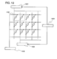
- This embodiment mode explains a method for changing the amount of a current applied to each light emitting element in a divided light emitting region with reference to FIG 12.
- a divided light emitting region 1301 includes two light emitting elements. Each light emitting element is controlled based on signals inputted from a first control circuit 1302 and a second control circuit 1303. In addition, the luminance of each light emitting element is determined depending on the values of currents supplied from the first control circuit 1302 and the second control circuit 1303. The values of currents supplied from the first control circuit 1302 and the second control circuit 1303 determine the amount of a current to be applied to the light emitting element depending on the degree of change over time of the light emitting element, which is calculated by a monitor circuit 1304.
- a change in emission color of each light emitting element over time is calculated using a monitoring light emitting element or using a result of lighting time of the light emitting element and pre-measured deterioration characteristics of the light emitting element.
- the degree of change over time which is calculated by the monitor circuit 1304 is inputted to the first control circuit 1302 and the second control circuit 1303 to determine the amount of a current to be supplied to each light emitting element.
- signals from a memory in which pre-measured deterioration characteristics over time of the light emitting element are recorded and a timer which measures light emitting time are inputted into the monitor circuit 1304, and the degree of change over time which is calculated by the monitor circuit 1304 is inputted into the first control circuit 1302 and the second control circuit 1303 to determine the amount of a current to be supplied to each light emitting element.
- luminances of a plurality of light emitting elements in a divided light emitting region can be controlled independently, so that an emission color can be controlled so as to maintain an emission color of the divided light emitting region.
- the emission color and luminance of the light emitting region as a whole can be maintained.
- a tone of the emission color can be changed by using a control means (such as a control circuit, a power supply circuit, or a monitor circuit).
- FIG 12 shows only light emitting elements in the divided light emitting region 1301, but a thin film transistor (TFT) may be formed as a control means which controls light emission of the light emitting element.
- TFT thin film transistor
- This embodiment mode explains a structure of a light emitting region of the lighting system of the present invention. Explanation is made with reference to FIG 6.
- a light emitting region is divided into a plurality of regions and each of the divided light emitting regions includes a plurality of light emitting elements.
- FIG 6 shows one mode of the lighting system of the present invention.
- a light emitting region 601 a first circuit portion 604, and a second circuit portion 605 are provided over a substrate 600.
- the divided light emitting regions are arranged in matrix, and one divided light emitting region 607 is provided with two light emitting elements.
- each light emitting element is electrically connected to both the first circuit portion 604 and the second circuit portion 605.
- each light emitting element is electrically connected to an IC 608 where a power supply circuit, a monitor circuit, and the like are formed, through an FPC 606.
- a control means such as a control circuit, a power supply circuit, or a monitor circuit
- the size of each divided light emitting region is preferably sufficiently small so that a difference between emission colors of the first light emitting element 602 and the second light emitting element 603 is unnoticeable.
- FIG 6 shows the lighting system in which the first circuit portion 604 and the second circuit portion 605 are formed over a substrate where the light emitting region 601 is formed, the first circuit portion and the second circuit portion may be formed on an IC and may be mounted.
- the lighting system of the present invention can emit light with high luminance, causes little color shift even after being used for a long time, and has a long life.
- this embodiment mode explains a lighting system having a structure different from that described in Embodiment Mode 8.
- a light emitting region is divided into a plurality of regions, and each of the divided light emitting regions includes a plurality of light emitting elements.
- FIG 7 shows one mode of the lighting system of the present invention.
- a light emitting region 701 a first circuit portion 704, and a second circuit portion 705 are provided over a substrate 700.
- a plurality of divided light emitting regions is arranged in stripes, and one divided light emitting region 707 includes two light emitting elements.
- each light emitting element is electrically connected to both the first circuit portion 704 and the second circuit portion 705.
- each light emitting element is electrically connected to an IC 708 where a power supply circuit, a monitor circuit, and the like are formed, through an FPC 706.
- a control means such as a control circuit, a power supply circuit, or a monitor circuit
- the size of each divided light emitting region is preferably sufficiently small so that a difference between emission colors of the first light emitting element 702 and the second light emitting element 703 is unnoticeable.
- the width of the divided light emitting region 707 is preferably sufficiently small so that the difference between emission colors of the first light emitting element and the second light emitting element is not recognized by human eyes. Since the divided light emitting regions are arranged linearly as shown in FIG 7, simplification of a process and cost reduction can be achieved.
- FIG 7 shows the lighting system in which the first circuit portion 704 and the second circuit portion 705 are formed over a substrate where the light emitting region 701 is formed
- the first circuit portion and the second circuit portion may be formed on an IC and may be mounted.
- the lighting system of the present invention can emit light with high luminance, causes little color shift even after being used for a long time, and has a long life.
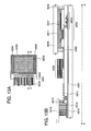
- FIG 13A is a top view of a panel in which a thin film transistor (TFT) and a light emitting element formed over an element substrate are sealed with a sealant between the element substrate and a cover material.
- FIG 13B corresponds to a cross-sectional view of FIG 13A taken along a line A-A'.
- TFT thin film transistor
- a sealant 4005 is provided to surround a light emitting region 4002 and a gate line driver circuit 4004 which are provided over an element substrate 4001.
- a cover material 4006 is provided over the light emitting region 4002 and the gate line driver circuit 4004.
- the light emitting region 4002 and the gate line driver circuit 4004 as well as a filler 4007 are sealed with the element substrate 4001, the sealant 4005, and the cover material 4006.
- an IC where a source line driver circuit 4003 is formed is mounted on the element substrate 4001 in a region other than the region surrounded by the sealant 4005.
- the light emitting region 4002 and the gate line driver circuit 4004 which are provided over the element substrate 4001 include a plurality of TFTs.
- FIG 13B shows a TFT 4010 included in the light emitting region 4002 as an example.
- the TFT 4010 is formed using an amorphous semiconductor, and a source region or a drain region of the TFT 4010 is electrically connected to a light emitting element 4011.
- connection terminal 4016 various signals and potentials supplied to the source line driver circuit 4003 which is formed separately and the gate line driver circuit 4004 or the light emitting region 4002 are supplied from a connection terminal 4016 through lead wires 4014 and 4015.
- the connection terminal 4016 and the lead wires 4014 and 4015 can be formed by various methods.
- connection terminal 4016 is electrically connected to a terminal included in a flexible printed circuit (FPC) 4018 through an anisotropic conductive film 4019.
- FPC flexible printed circuit
- glass glass, metal (typically, stainless steel), ceramic, or plastic can be used as the element substrate 4001 and the cover material 4006.
- plastic an FRP (Fiberglass-Reinforced Plastics) plate, a PVF (polyvinyl fluoride) film, a mylar film, a polyester film, or an acrylic resin film can be used.
- FRP Fiberlass-Reinforced Plastics
- PVF polyvinyl fluoride
- mylar film a polyester film
- acrylic resin film acrylic resin film
- a sheet with a structure in which an aluminum foil is sandwiched between PVF films or mylar films can be used.
- a cover material located in an extraction direction of light from the light emitting element 4011 needs to be transparent.
- a light transmitting material such as a glass plate, a plastic plate, a polyester film, or an acrylic film is used.
- An ultraviolet curing resin or a thermosetting resin as well as an inert gas such as nitrogen or argon can be used as the filler 4007.
- PVC polyvinyl chloride
- acrylic polyimide
- an epoxy resin a silicon resin
- PVB polyvinyl butyral
- EVA ethylene vinyl acetate
- an inert liquid such as carbon fluoride may be used.
- a hygroscopic substance preferably, barium oxide
- a substance capable of adsorbing oxygen as well as the filler 4007 may be provided between the cover material 4006 and the element substrate 4001.
- FIGS. 13A and 13B show the mode in which the source line driver circuit 4003 is formed separately and mounted on the element substrate 4001, but the present invention is not limited to this structure.
- the gate line driver circuit may be separately formed and then mounted, or only a part of the source line driver circuit or the gate line driver circuit may be separately formed and then mounted.
- all of the source line driver circuit, the gate line driver circuit, a controller, a power supply circuit, a monitor circuit, and the like may be formed on an IC and then mounted.
- this embodiment mode describes the lighting system which includes a TFT using an amorphous semiconductor as one mode.
- the source line driver circuit, the gate line driver circuit, and the like may be formed over the same substrate as that provided with TFTs of a light emitting region.
- a large-area lighting system may be manufactured by attaching a peeled panel.
- a transistor used for the lighting system of the present invention may use either an organic semiconductor or an inorganic semiconductor. Alternatively, it may use an amorphous semiconductor, a microcrystalline semiconductor, a crystalline semiconductor, or the like.
- This embodiment mode explains modes of devices using the lighting system of the present invention with reference to FIGS. 9 and 10A to 10C.
- FIG 9 shows an example of a liquid crystal display device using the lighting system of the present invention as a backlight.
- the liquid crystal display device shown in FIG 9 includes a chassis 901, a liquid crystal layer 902, a backlight 903, and a chassis 904.
- the liquid crystal layer 902 is connected to a driver IC 905.
- the lighting system of the present invention is used as the backlight 903 , to which a current is supplied through a terminal 906.
- the lighting system of the present invention as a backlight of a liquid crystal display device, a backlight with high luminance and long life can be obtained, which improves quality as a display device. Since the lighting system of the present invention is a plane-emission lighting system and can be formed to have a large area, a larger-area backlight can be obtained and a larger-area liquid crystal display device can also be obtained. Furthermore, a light emitting element is thin and consumes less power; therefore, reductions in thickness and power consumption of the display device can also be achieved.
- FIG. 10A shows the lighting system of the present invention used as indoor lighting. Since the lighting system of the present invention has high luminance, the lighting system can light a room more brightly. In addition, since the lighting system of the present invention has a long life, the frequency of replacing lighting systems can be decreased.
- the lighting system of the present invention is a plane-emission lighting system and can be formed to have a large area. Therefore, for example, an entire ceiling can be provided with the lighting system of the present invention. Not only the ceiling but also a wall, a floor, a column, or the like can be provided with the lighting system of the present invention. Furthermore, by manufacturing the lighting system of the present invention using a flexible substrate, a thin and flexible lighting system can be obtained. Thus, the lighting system of the present invention can also be provided over a curved surface. Moreover, the lighting system can be used not only indoors but also outdoors and can be provided on a building wall or the like as an outdoor light.
- FIG 10B shows the lighting system of the present invention used as lighting in a tunnel. Since the lighting system of the present invention has high luminance, it can light the inside of a tunnel more brightly. In addition, since the lighting system of the present invention has a long life, the frequency of replacing lighting systems can be decreased and maintenance cost can be reduced. Furthermore, by manufacturing the lighting system of the present invention using a flexible substrate, a thin and flexible lighting system can be obtained. Therefore, the lighting system of the present invention can be formed along a curved inner wall of a tunnel.
- FIG. 10C shows an example of the lighting system of the present invention used as interior lighting. Since the lighting system of the present invention has high luminance, it can light a space around it more brightly. In addition, since the lighting system of the present invention has a long life, the frequency of replacing lighting systems can be decreased. Furthermore, by manufacturing the lighting system of the present invention using a flexible substrate, a thin and flexible lighting system can be obtained. Since the lighting system of the present invention is of a plane-emission type, it can be processed into a desired shape as shown in FIG 10C.
- the lighting system of the present invention can also be used as lighting in taking a picture.
- a picture similar to one which is taken with a subject illuminated by natural light can be taken when a subject is illuminated by large-area light with high luminance.
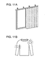
- FIG 11A shows a curtain-shaped lighting system.
- a thin and flexible lighting system can be obtained.
- outside light can be let into a room by tying the curtain-shaped lighting system, and at night, the room can be lit by spreading the curtain-shaped lighting system, similarly to the case of letting in outside light.
- the lighting system of the present invention has high luminance, it can light a room more brightly.
- the frequency of replacing lighting systems can be decreased.
- FIG 11B shows clothing using the lighting system of the present invention in part thereof.
- a thin and flexible lighting system can be obtained.
- a power source a solar battery may be used, or a battery may be mounted.
- the lighting system of the present invention can be used for clothing goods such as a bag and a hat, and the like as well as clothing. Since the lighting system of the present invention has high luminance, it enables a person far away to recognize the presence of a wearer.
Landscapes
- Physics & Mathematics (AREA)
- Engineering & Computer Science (AREA)
- Optics & Photonics (AREA)
- Computer Hardware Design (AREA)
- General Physics & Mathematics (AREA)
- Theoretical Computer Science (AREA)
- Electroluminescent Light Sources (AREA)
- Circuit Arrangement For Electric Light Sources In General (AREA)
- Planar Illumination Modules (AREA)
- Illuminated Signs And Luminous Advertising (AREA)
Applications Claiming Priority (1)
| Application Number | Priority Date | Filing Date | Title |
|---|---|---|---|
| JP2005301837 | 2005-10-17 |
Publications (2)
| Publication Number | Publication Date |
|---|---|
| EP1784055A2 true EP1784055A2 (fr) | 2007-05-09 |
| EP1784055A3 EP1784055A3 (fr) | 2009-08-05 |
Family
ID=37635784
Family Applications (1)
| Application Number | Title | Priority Date | Filing Date |
|---|---|---|---|
| EP06021358A Withdrawn EP1784055A3 (fr) | 2005-10-17 | 2006-10-11 | Système d' éclairage |
Country Status (5)
| Country | Link |
|---|---|
| US (2) | US8154192B2 (fr) |
| EP (1) | EP1784055A3 (fr) |
| JP (2) | JP5121989B2 (fr) |
| CN (2) | CN102143622B (fr) |
| TW (2) | TWI625068B (fr) |
Cited By (56)
| Publication number | Priority date | Publication date | Assignee | Title |
|---|---|---|---|---|
| EP2267690A1 (fr) * | 2009-06-16 | 2010-12-29 | Ignis Innovation Inc. | Technique de compensation de la distorsion de couleurs dans des affichages |
| US8743096B2 (en) | 2006-04-19 | 2014-06-03 | Ignis Innovation, Inc. | Stable driving scheme for active matrix displays |
| US8816946B2 (en) | 2004-12-15 | 2014-08-26 | Ignis Innovation Inc. | Method and system for programming, calibrating and driving a light emitting device display |
| US8907991B2 (en) | 2010-12-02 | 2014-12-09 | Ignis Innovation Inc. | System and methods for thermal compensation in AMOLED displays |
| USRE45291E1 (en) | 2004-06-29 | 2014-12-16 | Ignis Innovation Inc. | Voltage-programming scheme for current-driven AMOLED displays |
| US8922544B2 (en) | 2012-05-23 | 2014-12-30 | Ignis Innovation Inc. | Display systems with compensation for line propagation delay |
| US8941697B2 (en) | 2003-09-23 | 2015-01-27 | Ignis Innovation Inc. | Circuit and method for driving an array of light emitting pixels |
| US8994617B2 (en) | 2010-03-17 | 2015-03-31 | Ignis Innovation Inc. | Lifetime uniformity parameter extraction methods |
| US9059117B2 (en) | 2009-12-01 | 2015-06-16 | Ignis Innovation Inc. | High resolution pixel architecture |
| US9093029B2 (en) | 2011-05-20 | 2015-07-28 | Ignis Innovation Inc. | System and methods for extraction of threshold and mobility parameters in AMOLED displays |
| US9093028B2 (en) | 2009-12-06 | 2015-07-28 | Ignis Innovation Inc. | System and methods for power conservation for AMOLED pixel drivers |
| US9125278B2 (en) | 2006-08-15 | 2015-09-01 | Ignis Innovation Inc. | OLED luminance degradation compensation |
| US9171504B2 (en) | 2013-01-14 | 2015-10-27 | Ignis Innovation Inc. | Driving scheme for emissive displays providing compensation for driving transistor variations |
| US9171500B2 (en) | 2011-05-20 | 2015-10-27 | Ignis Innovation Inc. | System and methods for extraction of parasitic parameters in AMOLED displays |
| US9275579B2 (en) | 2004-12-15 | 2016-03-01 | Ignis Innovation Inc. | System and methods for extraction of threshold and mobility parameters in AMOLED displays |
| US9280933B2 (en) | 2004-12-15 | 2016-03-08 | Ignis Innovation Inc. | System and methods for extraction of threshold and mobility parameters in AMOLED displays |
| US9305488B2 (en) | 2013-03-14 | 2016-04-05 | Ignis Innovation Inc. | Re-interpolation with edge detection for extracting an aging pattern for AMOLED displays |
| US9311859B2 (en) | 2009-11-30 | 2016-04-12 | Ignis Innovation Inc. | Resetting cycle for aging compensation in AMOLED displays |
| US9324268B2 (en) | 2013-03-15 | 2016-04-26 | Ignis Innovation Inc. | Amoled displays with multiple readout circuits |
| US9336717B2 (en) | 2012-12-11 | 2016-05-10 | Ignis Innovation Inc. | Pixel circuits for AMOLED displays |
| US9343006B2 (en) | 2012-02-03 | 2016-05-17 | Ignis Innovation Inc. | Driving system for active-matrix displays |
| US9384698B2 (en) | 2009-11-30 | 2016-07-05 | Ignis Innovation Inc. | System and methods for aging compensation in AMOLED displays |
| US9430958B2 (en) | 2010-02-04 | 2016-08-30 | Ignis Innovation Inc. | System and methods for extracting correlation curves for an organic light emitting device |
| US9437137B2 (en) | 2013-08-12 | 2016-09-06 | Ignis Innovation Inc. | Compensation accuracy |
| US9466240B2 (en) | 2011-05-26 | 2016-10-11 | Ignis Innovation Inc. | Adaptive feedback system for compensating for aging pixel areas with enhanced estimation speed |
| US9530349B2 (en) | 2011-05-20 | 2016-12-27 | Ignis Innovations Inc. | Charged-based compensation and parameter extraction in AMOLED displays |
| US9741282B2 (en) | 2013-12-06 | 2017-08-22 | Ignis Innovation Inc. | OLED display system and method |
| US9747834B2 (en) | 2012-05-11 | 2017-08-29 | Ignis Innovation Inc. | Pixel circuits including feedback capacitors and reset capacitors, and display systems therefore |
| US9761170B2 (en) | 2013-12-06 | 2017-09-12 | Ignis Innovation Inc. | Correction for localized phenomena in an image array |
| US9773439B2 (en) | 2011-05-27 | 2017-09-26 | Ignis Innovation Inc. | Systems and methods for aging compensation in AMOLED displays |
| US9786209B2 (en) | 2009-11-30 | 2017-10-10 | Ignis Innovation Inc. | System and methods for aging compensation in AMOLED displays |
| US9786223B2 (en) | 2012-12-11 | 2017-10-10 | Ignis Innovation Inc. | Pixel circuits for AMOLED displays |
| US9799246B2 (en) | 2011-05-20 | 2017-10-24 | Ignis Innovation Inc. | System and methods for extraction of threshold and mobility parameters in AMOLED displays |
| US9830857B2 (en) | 2013-01-14 | 2017-11-28 | Ignis Innovation Inc. | Cleaning common unwanted signals from pixel measurements in emissive displays |
| US9881532B2 (en) | 2010-02-04 | 2018-01-30 | Ignis Innovation Inc. | System and method for extracting correlation curves for an organic light emitting device |
| US9947293B2 (en) | 2015-05-27 | 2018-04-17 | Ignis Innovation Inc. | Systems and methods of reduced memory bandwidth compensation |
| US10013907B2 (en) | 2004-12-15 | 2018-07-03 | Ignis Innovation Inc. | Method and system for programming, calibrating and/or compensating, and driving an LED display |
| US10012678B2 (en) | 2004-12-15 | 2018-07-03 | Ignis Innovation Inc. | Method and system for programming, calibrating and/or compensating, and driving an LED display |
| US10019941B2 (en) | 2005-09-13 | 2018-07-10 | Ignis Innovation Inc. | Compensation technique for luminance degradation in electro-luminance devices |
| US10074304B2 (en) | 2015-08-07 | 2018-09-11 | Ignis Innovation Inc. | Systems and methods of pixel calibration based on improved reference values |
| US10078984B2 (en) | 2005-02-10 | 2018-09-18 | Ignis Innovation Inc. | Driving circuit for current programmed organic light-emitting diode displays |
| US10089921B2 (en) | 2010-02-04 | 2018-10-02 | Ignis Innovation Inc. | System and methods for extracting correlation curves for an organic light emitting device |
| US10089924B2 (en) | 2011-11-29 | 2018-10-02 | Ignis Innovation Inc. | Structural and low-frequency non-uniformity compensation |
| US10163401B2 (en) | 2010-02-04 | 2018-12-25 | Ignis Innovation Inc. | System and methods for extracting correlation curves for an organic light emitting device |
| US10176736B2 (en) | 2010-02-04 | 2019-01-08 | Ignis Innovation Inc. | System and methods for extracting correlation curves for an organic light emitting device |
| US10181282B2 (en) | 2015-01-23 | 2019-01-15 | Ignis Innovation Inc. | Compensation for color variations in emissive devices |
| US10192479B2 (en) | 2014-04-08 | 2019-01-29 | Ignis Innovation Inc. | Display system using system level resources to calculate compensation parameters for a display module in a portable device |
| US10235933B2 (en) | 2005-04-12 | 2019-03-19 | Ignis Innovation Inc. | System and method for compensation of non-uniformities in light emitting device displays |
| US10311780B2 (en) | 2015-05-04 | 2019-06-04 | Ignis Innovation Inc. | Systems and methods of optical feedback |
| US10319307B2 (en) | 2009-06-16 | 2019-06-11 | Ignis Innovation Inc. | Display system with compensation techniques and/or shared level resources |
| US10388221B2 (en) | 2005-06-08 | 2019-08-20 | Ignis Innovation Inc. | Method and system for driving a light emitting device display |
| US10439159B2 (en) | 2013-12-25 | 2019-10-08 | Ignis Innovation Inc. | Electrode contacts |
| US10573231B2 (en) | 2010-02-04 | 2020-02-25 | Ignis Innovation Inc. | System and methods for extracting correlation curves for an organic light emitting device |
| US10867536B2 (en) | 2013-04-22 | 2020-12-15 | Ignis Innovation Inc. | Inspection system for OLED display panels |
| US10996258B2 (en) | 2009-11-30 | 2021-05-04 | Ignis Innovation Inc. | Defect detection and correction of pixel circuits for AMOLED displays |
| EP3203138B1 (fr) * | 2016-02-04 | 2021-11-17 | Valeo Vision | Didpositif d'eclairage ou de de signalisation pour vehicule automobile |
Families Citing this family (12)
| Publication number | Priority date | Publication date | Assignee | Title |
|---|---|---|---|---|
| CN100544535C (zh) * | 2004-04-28 | 2009-09-23 | 株式会社半导体能源研究所 | 发光元件及其制造方法,以及利用该发光元件的发光器件 |
| EP1784055A3 (fr) * | 2005-10-17 | 2009-08-05 | Semiconductor Energy Laboratory Co., Ltd. | Système d' éclairage |
| WO2010062643A1 (fr) * | 2008-10-28 | 2010-06-03 | The Regents Of The University Of Michigan | Oled blanche empilée présentant des sous-éléments rouges, verts et bleus séparés |
| DE102013208844A1 (de) | 2012-06-01 | 2013-12-05 | Semiconductor Energy Laboratory Co., Ltd. | Lichtemittierendes Element, lichtemittierende Vorrichtung, Anzeigevorrichtung, elektronisches Gerät und Beleuchtungsvorrichtung |
| US10032834B2 (en) * | 2012-08-09 | 2018-07-24 | Sony Corporation | Light receiving/emitting element and light receiving/emitting apparatus |
| US9420662B2 (en) | 2012-09-05 | 2016-08-16 | Pioneer Corporation | Light-emitting device |
| JP6091166B2 (ja) * | 2012-11-08 | 2017-03-08 | 株式会社カネカ | 有機el装置 |
| CN103730586B (zh) * | 2013-12-31 | 2015-12-02 | 京东方科技集团股份有限公司 | 层叠式有机发光二极体及其制备方法 |
| DE102014111346B4 (de) * | 2014-08-08 | 2022-11-03 | Pictiva Displays International Limited | Optoelektronische Bauelementevorrichtung und Verfahren zum Herstellen einer optoelektronischen Bauelementevorrichtung |
| WO2019050939A1 (fr) * | 2017-09-08 | 2019-03-14 | Lumileds Llc | Dispositif optoélectronique et système d'éclairage adaptatif l'utilisant |
| US9974135B1 (en) | 2017-09-08 | 2018-05-15 | Lumileds Llc | Optoelectronic device and adaptive illumination system using the same |
| JP7307535B2 (ja) * | 2018-10-26 | 2023-07-12 | シーシーエス株式会社 | Oled駆動システム |
Family Cites Families (58)
| Publication number | Priority date | Publication date | Assignee | Title |
|---|---|---|---|---|
| JP3366401B2 (ja) | 1992-11-20 | 2003-01-14 | 出光興産株式会社 | 白色有機エレクトロルミネッセンス素子 |
| US5703436A (en) * | 1994-12-13 | 1997-12-30 | The Trustees Of Princeton University | Transparent contacts for organic devices |
| JP4477150B2 (ja) * | 1996-01-17 | 2010-06-09 | 三星モバイルディスプレイ株式會社 | 有機薄膜el素子 |
| JP4486713B2 (ja) | 1997-01-27 | 2010-06-23 | 淳二 城戸 | 有機エレクトロルミネッセント素子 |
| JPH10270171A (ja) * | 1997-01-27 | 1998-10-09 | Junji Kido | 有機エレクトロルミネッセント素子 |
| US5932895A (en) * | 1997-05-20 | 1999-08-03 | The Trustees Of Princeton University | Saturated full color stacked organic light emitting devices |
| JP3884564B2 (ja) * | 1998-05-20 | 2007-02-21 | 出光興産株式会社 | 有機el発光素子およびそれを用いた発光装置 |
| JP2000057935A (ja) * | 1998-08-10 | 2000-02-25 | Pioneer Electron Corp | 電子放出発光素子及びこれを用いた表示装置 |
| JP3287344B2 (ja) * | 1998-10-09 | 2002-06-04 | 株式会社デンソー | 有機el素子 |
| JP2000349345A (ja) * | 1999-06-04 | 2000-12-15 | Matsushita Electronics Industry Corp | 半導体発光装置 |
| JP2001135479A (ja) * | 1999-11-08 | 2001-05-18 | Canon Inc | 発光素子、並びにそれを用いた画像読取装置、情報処理装置及びディスプレイ装置 |
| JP2001188513A (ja) * | 1999-12-28 | 2001-07-10 | Matsushita Electric Ind Co Ltd | 表示装置 |
| JP2002260859A (ja) | 2001-02-28 | 2002-09-13 | Matsushita Electric Ind Co Ltd | 照明装置 |
| JP2002278506A (ja) | 2001-03-19 | 2002-09-27 | Sharp Corp | 発光輝度調整手段を備えた発光装置及び該発光装置を用いた表示装置 |
| EP1393293B1 (fr) * | 2001-04-04 | 2010-11-17 | Siemens Aktiengesellschaft | Compensation du vieillissement dans des ecrans a diodes electroluminescentes organiques (oled) |
| JP4611578B2 (ja) | 2001-07-26 | 2011-01-12 | 淳二 城戸 | 有機エレクトロルミネッセント素子 |
| US6456016B1 (en) * | 2001-07-30 | 2002-09-24 | Intel Corporation | Compensating organic light emitting device displays |
| US6555967B2 (en) * | 2001-09-19 | 2003-04-29 | Supertex, Inc. | Low noise method and apparatus for driving electroluminescent panels |
| TW519852B (en) * | 2001-10-18 | 2003-02-01 | Opto Tech Corp | Organic light emitting device capable of projecting white light source and its manufacturing method |
| JP2003264085A (ja) | 2001-12-05 | 2003-09-19 | Semiconductor Energy Lab Co Ltd | 有機半導体素子、有機エレクトロルミネッセンス素子及び有機太陽電池 |
| SG142163A1 (en) * | 2001-12-05 | 2008-05-28 | Semiconductor Energy Lab | Organic semiconductor element |
| US6872472B2 (en) * | 2002-02-15 | 2005-03-29 | Eastman Kodak Company | Providing an organic electroluminescent device having stacked electroluminescent units |
| JP3933591B2 (ja) * | 2002-03-26 | 2007-06-20 | 淳二 城戸 | 有機エレクトロルミネッセント素子 |
| JP2003303683A (ja) * | 2002-04-09 | 2003-10-24 | Semiconductor Energy Lab Co Ltd | 発光装置 |
| JP4211291B2 (ja) | 2002-06-03 | 2009-01-21 | 株式会社豊田自動織機 | 有機エレクトロルミネッセンス素子 |
| TWI272874B (en) * | 2002-08-09 | 2007-02-01 | Semiconductor Energy Lab | Organic electroluminescent device |
| EP1388903B1 (fr) * | 2002-08-09 | 2016-03-16 | Semiconductor Energy Laboratory Co., Ltd. | Dispositif électroluminescent organique |
| US6747618B2 (en) * | 2002-08-20 | 2004-06-08 | Eastman Kodak Company | Color organic light emitting diode display with improved lifetime |
| JP3717879B2 (ja) * | 2002-09-30 | 2005-11-16 | 三洋電機株式会社 | 発光素子 |
| CN100580753C (zh) * | 2002-11-29 | 2010-01-13 | 株式会社半导体能源研究所 | 显示装置和电子装置 |
| US7230594B2 (en) * | 2002-12-16 | 2007-06-12 | Eastman Kodak Company | Color OLED display with improved power efficiency |
| JP4069745B2 (ja) * | 2002-12-26 | 2008-04-02 | 株式会社デンソー | 有機elパネル |
| CN1742518B (zh) * | 2003-01-29 | 2010-09-29 | 株式会社半导体能源研究所 | 发光装置 |
| US7161566B2 (en) * | 2003-01-31 | 2007-01-09 | Eastman Kodak Company | OLED display with aging compensation |
| JP4531342B2 (ja) * | 2003-03-17 | 2010-08-25 | 株式会社半導体エネルギー研究所 | 白色有機発光素子および発光装置 |
| JP4477400B2 (ja) | 2003-04-07 | 2010-06-09 | 株式会社半導体エネルギー研究所 | 発光装置及び電子機器 |
| TWI363573B (en) * | 2003-04-07 | 2012-05-01 | Semiconductor Energy Lab | Electronic apparatus |
| JP4578846B2 (ja) | 2003-04-09 | 2010-11-10 | 株式会社半導体エネルギー研究所 | 白色発光素子および発光装置 |
| US7862906B2 (en) * | 2003-04-09 | 2011-01-04 | Semiconductor Energy Laboratory Co., Ltd. | Electroluminescent element and light-emitting device |
| US6771028B1 (en) * | 2003-04-30 | 2004-08-03 | Eastman Kodak Company | Drive circuitry for four-color organic light-emitting device |
| US6936961B2 (en) * | 2003-05-13 | 2005-08-30 | Eastman Kodak Company | Cascaded organic electroluminescent device having connecting units with N-type and P-type organic layers |
| US6909233B2 (en) * | 2003-06-11 | 2005-06-21 | Eastman Kodak Company | Stacked OLED display having improved efficiency |
| US7019662B2 (en) * | 2003-07-29 | 2006-03-28 | Universal Lighting Technologies, Inc. | LED drive for generating constant light output |
| US7504049B2 (en) * | 2003-08-25 | 2009-03-17 | Semiconductor Energy Laboratory Co., Ltd. | Electrode device for organic device, electronic device having electrode device for organic device, and method of forming electrode device for organic device |
| US7511421B2 (en) * | 2003-08-25 | 2009-03-31 | Semiconductor Energy Laboratory Co., Ltd. | Mixed metal and organic electrode for organic device |
| KR100552968B1 (ko) * | 2003-09-23 | 2006-02-15 | 삼성에스디아이 주식회사 | 액티브 매트릭스 유기전계 발광표시장치 |
| US7015504B2 (en) * | 2003-11-03 | 2006-03-21 | Advanced Micro Devices, Inc. | Sidewall formation for high density polymer memory element array |
| JP4431379B2 (ja) | 2003-12-19 | 2010-03-10 | 東北パイオニア株式会社 | 有機el素子及びその形成方法 |
| US7333080B2 (en) * | 2004-03-29 | 2008-02-19 | Eastman Kodak Company | Color OLED display with improved power efficiency |
| CN100557667C (zh) * | 2004-04-22 | 2009-11-04 | 株式会社半导体能源研究所 | 发光装置及其驱动方法 |
| US20050242712A1 (en) * | 2004-04-29 | 2005-11-03 | Chao-Chin Sung | Multicolor electroluminescent display |
| WO2005115062A1 (fr) * | 2004-05-20 | 2005-12-01 | Semiconductor Energy Laboratory Co., Ltd. | Élément luminescent et dispositif d’affichage |
| KR101215279B1 (ko) * | 2004-05-21 | 2012-12-26 | 가부시키가이샤 한도오따이 에네루기 켄큐쇼 | 조명 장치 |
| KR101152935B1 (ko) * | 2004-05-21 | 2012-06-08 | 가부시키가이샤 한도오따이 에네루기 켄큐쇼 | 발광소자 및 발광장치 |
| US7528810B2 (en) * | 2004-05-25 | 2009-05-05 | Victor Company Of Japan, Limited | Display with multiple emission layers |
| US7227305B2 (en) * | 2004-06-18 | 2007-06-05 | General Electric Company | Stacked organic electroluminescent devices |
| US7737626B2 (en) * | 2004-09-30 | 2010-06-15 | Semiconductor Energy Laboratory Co., Ltd. | Light emitting element |
| EP1784055A3 (fr) * | 2005-10-17 | 2009-08-05 | Semiconductor Energy Laboratory Co., Ltd. | Système d' éclairage |
-
2006
- 2006-10-11 EP EP06021358A patent/EP1784055A3/fr not_active Withdrawn
- 2006-10-12 US US11/580,200 patent/US8154192B2/en not_active Expired - Fee Related
- 2006-10-14 TW TW102126645A patent/TWI625068B/zh not_active IP Right Cessation
- 2006-10-14 TW TW095137907A patent/TWI429324B/zh not_active IP Right Cessation
- 2006-10-17 CN CN2010105868421A patent/CN102143622B/zh not_active Expired - Fee Related
- 2006-10-17 CN CN2006101318958A patent/CN1953625B/zh not_active Expired - Fee Related
-
2011
- 2011-08-02 JP JP2011168964A patent/JP5121989B2/ja not_active Expired - Fee Related
-
2012
- 2012-04-09 US US13/442,100 patent/US8441184B2/en not_active Expired - Fee Related
- 2012-09-26 JP JP2012211714A patent/JP5393861B2/ja not_active Expired - Fee Related
Cited By (124)
| Publication number | Priority date | Publication date | Assignee | Title |
|---|---|---|---|---|
| US10089929B2 (en) | 2003-09-23 | 2018-10-02 | Ignis Innovation Inc. | Pixel driver circuit with load-balance in current mirror circuit |
| US9472139B2 (en) | 2003-09-23 | 2016-10-18 | Ignis Innovation Inc. | Circuit and method for driving an array of light emitting pixels |
| US9472138B2 (en) | 2003-09-23 | 2016-10-18 | Ignis Innovation Inc. | Pixel driver circuit with load-balance in current mirror circuit |
| US9852689B2 (en) | 2003-09-23 | 2017-12-26 | Ignis Innovation Inc. | Circuit and method for driving an array of light emitting pixels |
| US8941697B2 (en) | 2003-09-23 | 2015-01-27 | Ignis Innovation Inc. | Circuit and method for driving an array of light emitting pixels |
| USRE47257E1 (en) | 2004-06-29 | 2019-02-26 | Ignis Innovation Inc. | Voltage-programming scheme for current-driven AMOLED displays |
| USRE45291E1 (en) | 2004-06-29 | 2014-12-16 | Ignis Innovation Inc. | Voltage-programming scheme for current-driven AMOLED displays |
| US9275579B2 (en) | 2004-12-15 | 2016-03-01 | Ignis Innovation Inc. | System and methods for extraction of threshold and mobility parameters in AMOLED displays |
| US9280933B2 (en) | 2004-12-15 | 2016-03-08 | Ignis Innovation Inc. | System and methods for extraction of threshold and mobility parameters in AMOLED displays |
| US10013907B2 (en) | 2004-12-15 | 2018-07-03 | Ignis Innovation Inc. | Method and system for programming, calibrating and/or compensating, and driving an LED display |
| US9970964B2 (en) | 2004-12-15 | 2018-05-15 | Ignis Innovation Inc. | Method and system for programming, calibrating and driving a light emitting device display |
| US8994625B2 (en) | 2004-12-15 | 2015-03-31 | Ignis Innovation Inc. | Method and system for programming, calibrating and driving a light emitting device display |
| US10012678B2 (en) | 2004-12-15 | 2018-07-03 | Ignis Innovation Inc. | Method and system for programming, calibrating and/or compensating, and driving an LED display |
| US10699624B2 (en) | 2004-12-15 | 2020-06-30 | Ignis Innovation Inc. | Method and system for programming, calibrating and/or compensating, and driving an LED display |
| US8816946B2 (en) | 2004-12-15 | 2014-08-26 | Ignis Innovation Inc. | Method and system for programming, calibrating and driving a light emitting device display |
| US10078984B2 (en) | 2005-02-10 | 2018-09-18 | Ignis Innovation Inc. | Driving circuit for current programmed organic light-emitting diode displays |
| US10235933B2 (en) | 2005-04-12 | 2019-03-19 | Ignis Innovation Inc. | System and method for compensation of non-uniformities in light emitting device displays |
| US10388221B2 (en) | 2005-06-08 | 2019-08-20 | Ignis Innovation Inc. | Method and system for driving a light emitting device display |
| US10019941B2 (en) | 2005-09-13 | 2018-07-10 | Ignis Innovation Inc. | Compensation technique for luminance degradation in electro-luminance devices |
| US10127860B2 (en) | 2006-04-19 | 2018-11-13 | Ignis Innovation Inc. | Stable driving scheme for active matrix displays |
| US10453397B2 (en) | 2006-04-19 | 2019-10-22 | Ignis Innovation Inc. | Stable driving scheme for active matrix displays |
| US9633597B2 (en) | 2006-04-19 | 2017-04-25 | Ignis Innovation Inc. | Stable driving scheme for active matrix displays |
| US8743096B2 (en) | 2006-04-19 | 2014-06-03 | Ignis Innovation, Inc. | Stable driving scheme for active matrix displays |
| US9842544B2 (en) | 2006-04-19 | 2017-12-12 | Ignis Innovation Inc. | Stable driving scheme for active matrix displays |
| US9530352B2 (en) | 2006-08-15 | 2016-12-27 | Ignis Innovations Inc. | OLED luminance degradation compensation |
| US10325554B2 (en) | 2006-08-15 | 2019-06-18 | Ignis Innovation Inc. | OLED luminance degradation compensation |
| US9125278B2 (en) | 2006-08-15 | 2015-09-01 | Ignis Innovation Inc. | OLED luminance degradation compensation |
| US9117400B2 (en) | 2009-06-16 | 2015-08-25 | Ignis Innovation Inc. | Compensation technique for color shift in displays |
| US10553141B2 (en) | 2009-06-16 | 2020-02-04 | Ignis Innovation Inc. | Compensation technique for color shift in displays |
| US9111485B2 (en) | 2009-06-16 | 2015-08-18 | Ignis Innovation Inc. | Compensation technique for color shift in displays |
| US9418587B2 (en) | 2009-06-16 | 2016-08-16 | Ignis Innovation Inc. | Compensation technique for color shift in displays |
| EP2267690A1 (fr) * | 2009-06-16 | 2010-12-29 | Ignis Innovation Inc. | Technique de compensation de la distorsion de couleurs dans des affichages |
| US10319307B2 (en) | 2009-06-16 | 2019-06-11 | Ignis Innovation Inc. | Display system with compensation techniques and/or shared level resources |
| US10699613B2 (en) | 2009-11-30 | 2020-06-30 | Ignis Innovation Inc. | Resetting cycle for aging compensation in AMOLED displays |
| US10996258B2 (en) | 2009-11-30 | 2021-05-04 | Ignis Innovation Inc. | Defect detection and correction of pixel circuits for AMOLED displays |
| US9786209B2 (en) | 2009-11-30 | 2017-10-10 | Ignis Innovation Inc. | System and methods for aging compensation in AMOLED displays |
| US10679533B2 (en) | 2009-11-30 | 2020-06-09 | Ignis Innovation Inc. | System and methods for aging compensation in AMOLED displays |
| US10304390B2 (en) | 2009-11-30 | 2019-05-28 | Ignis Innovation Inc. | System and methods for aging compensation in AMOLED displays |
| US9311859B2 (en) | 2009-11-30 | 2016-04-12 | Ignis Innovation Inc. | Resetting cycle for aging compensation in AMOLED displays |
| US9384698B2 (en) | 2009-11-30 | 2016-07-05 | Ignis Innovation Inc. | System and methods for aging compensation in AMOLED displays |
| US9059117B2 (en) | 2009-12-01 | 2015-06-16 | Ignis Innovation Inc. | High resolution pixel architecture |
| US9262965B2 (en) | 2009-12-06 | 2016-02-16 | Ignis Innovation Inc. | System and methods for power conservation for AMOLED pixel drivers |
| US9093028B2 (en) | 2009-12-06 | 2015-07-28 | Ignis Innovation Inc. | System and methods for power conservation for AMOLED pixel drivers |
| US10032399B2 (en) | 2010-02-04 | 2018-07-24 | Ignis Innovation Inc. | System and methods for extracting correlation curves for an organic light emitting device |
| US10176736B2 (en) | 2010-02-04 | 2019-01-08 | Ignis Innovation Inc. | System and methods for extracting correlation curves for an organic light emitting device |
| US10971043B2 (en) | 2010-02-04 | 2021-04-06 | Ignis Innovation Inc. | System and method for extracting correlation curves for an organic light emitting device |
| US9773441B2 (en) | 2010-02-04 | 2017-09-26 | Ignis Innovation Inc. | System and methods for extracting correlation curves for an organic light emitting device |
| US9430958B2 (en) | 2010-02-04 | 2016-08-30 | Ignis Innovation Inc. | System and methods for extracting correlation curves for an organic light emitting device |
| US11200839B2 (en) | 2010-02-04 | 2021-12-14 | Ignis Innovation Inc. | System and methods for extracting correlation curves for an organic light emitting device |
| US10395574B2 (en) | 2010-02-04 | 2019-08-27 | Ignis Innovation Inc. | System and methods for extracting correlation curves for an organic light emitting device |
| US10573231B2 (en) | 2010-02-04 | 2020-02-25 | Ignis Innovation Inc. | System and methods for extracting correlation curves for an organic light emitting device |
| US9881532B2 (en) | 2010-02-04 | 2018-01-30 | Ignis Innovation Inc. | System and method for extracting correlation curves for an organic light emitting device |
| US10163401B2 (en) | 2010-02-04 | 2018-12-25 | Ignis Innovation Inc. | System and methods for extracting correlation curves for an organic light emitting device |
| US10089921B2 (en) | 2010-02-04 | 2018-10-02 | Ignis Innovation Inc. | System and methods for extracting correlation curves for an organic light emitting device |
| US8994617B2 (en) | 2010-03-17 | 2015-03-31 | Ignis Innovation Inc. | Lifetime uniformity parameter extraction methods |
| US8907991B2 (en) | 2010-12-02 | 2014-12-09 | Ignis Innovation Inc. | System and methods for thermal compensation in AMOLED displays |
| US9489897B2 (en) | 2010-12-02 | 2016-11-08 | Ignis Innovation Inc. | System and methods for thermal compensation in AMOLED displays |
| US9997110B2 (en) | 2010-12-02 | 2018-06-12 | Ignis Innovation Inc. | System and methods for thermal compensation in AMOLED displays |
| US10460669B2 (en) | 2010-12-02 | 2019-10-29 | Ignis Innovation Inc. | System and methods for thermal compensation in AMOLED displays |
| US10475379B2 (en) | 2011-05-20 | 2019-11-12 | Ignis Innovation Inc. | Charged-based compensation and parameter extraction in AMOLED displays |
| US10127846B2 (en) | 2011-05-20 | 2018-11-13 | Ignis Innovation Inc. | System and methods for extraction of threshold and mobility parameters in AMOLED displays |
| US9355584B2 (en) | 2011-05-20 | 2016-05-31 | Ignis Innovation Inc. | System and methods for extraction of threshold and mobility parameters in AMOLED displays |
| US10580337B2 (en) | 2011-05-20 | 2020-03-03 | Ignis Innovation Inc. | System and methods for extraction of threshold and mobility parameters in AMOLED displays |
| US9093029B2 (en) | 2011-05-20 | 2015-07-28 | Ignis Innovation Inc. | System and methods for extraction of threshold and mobility parameters in AMOLED displays |
| US9799246B2 (en) | 2011-05-20 | 2017-10-24 | Ignis Innovation Inc. | System and methods for extraction of threshold and mobility parameters in AMOLED displays |
| US9799248B2 (en) | 2011-05-20 | 2017-10-24 | Ignis Innovation Inc. | System and methods for extraction of threshold and mobility parameters in AMOLED displays |
| US9171500B2 (en) | 2011-05-20 | 2015-10-27 | Ignis Innovation Inc. | System and methods for extraction of parasitic parameters in AMOLED displays |
| US10325537B2 (en) | 2011-05-20 | 2019-06-18 | Ignis Innovation Inc. | System and methods for extraction of threshold and mobility parameters in AMOLED displays |
| US9589490B2 (en) | 2011-05-20 | 2017-03-07 | Ignis Innovation Inc. | System and methods for extraction of threshold and mobility parameters in AMOLED displays |
| US9530349B2 (en) | 2011-05-20 | 2016-12-27 | Ignis Innovations Inc. | Charged-based compensation and parameter extraction in AMOLED displays |
| US10032400B2 (en) | 2011-05-20 | 2018-07-24 | Ignis Innovation Inc. | System and methods for extraction of threshold and mobility parameters in AMOLED displays |
| US9466240B2 (en) | 2011-05-26 | 2016-10-11 | Ignis Innovation Inc. | Adaptive feedback system for compensating for aging pixel areas with enhanced estimation speed |
| US9978297B2 (en) | 2011-05-26 | 2018-05-22 | Ignis Innovation Inc. | Adaptive feedback system for compensating for aging pixel areas with enhanced estimation speed |
| US10706754B2 (en) | 2011-05-26 | 2020-07-07 | Ignis Innovation Inc. | Adaptive feedback system for compensating for aging pixel areas with enhanced estimation speed |
| US9640112B2 (en) | 2011-05-26 | 2017-05-02 | Ignis Innovation Inc. | Adaptive feedback system for compensating for aging pixel areas with enhanced estimation speed |
| US10417945B2 (en) | 2011-05-27 | 2019-09-17 | Ignis Innovation Inc. | Systems and methods for aging compensation in AMOLED displays |
| US9773439B2 (en) | 2011-05-27 | 2017-09-26 | Ignis Innovation Inc. | Systems and methods for aging compensation in AMOLED displays |
| US10089924B2 (en) | 2011-11-29 | 2018-10-02 | Ignis Innovation Inc. | Structural and low-frequency non-uniformity compensation |
| US10380944B2 (en) | 2011-11-29 | 2019-08-13 | Ignis Innovation Inc. | Structural and low-frequency non-uniformity compensation |
| US10043448B2 (en) | 2012-02-03 | 2018-08-07 | Ignis Innovation Inc. | Driving system for active-matrix displays |
| US9792857B2 (en) | 2012-02-03 | 2017-10-17 | Ignis Innovation Inc. | Driving system for active-matrix displays |
| US10453394B2 (en) | 2012-02-03 | 2019-10-22 | Ignis Innovation Inc. | Driving system for active-matrix displays |
| US9343006B2 (en) | 2012-02-03 | 2016-05-17 | Ignis Innovation Inc. | Driving system for active-matrix displays |
| US9747834B2 (en) | 2012-05-11 | 2017-08-29 | Ignis Innovation Inc. | Pixel circuits including feedback capacitors and reset capacitors, and display systems therefore |
| US9940861B2 (en) | 2012-05-23 | 2018-04-10 | Ignis Innovation Inc. | Display systems with compensation for line propagation delay |
| US9368063B2 (en) | 2012-05-23 | 2016-06-14 | Ignis Innovation Inc. | Display systems with compensation for line propagation delay |
| US9741279B2 (en) | 2012-05-23 | 2017-08-22 | Ignis Innovation Inc. | Display systems with compensation for line propagation delay |
| US10176738B2 (en) | 2012-05-23 | 2019-01-08 | Ignis Innovation Inc. | Display systems with compensation for line propagation delay |
| US8922544B2 (en) | 2012-05-23 | 2014-12-30 | Ignis Innovation Inc. | Display systems with compensation for line propagation delay |
| US9536460B2 (en) | 2012-05-23 | 2017-01-03 | Ignis Innovation Inc. | Display systems with compensation for line propagation delay |
| US9336717B2 (en) | 2012-12-11 | 2016-05-10 | Ignis Innovation Inc. | Pixel circuits for AMOLED displays |
| US9685114B2 (en) | 2012-12-11 | 2017-06-20 | Ignis Innovation Inc. | Pixel circuits for AMOLED displays |
| US10311790B2 (en) | 2012-12-11 | 2019-06-04 | Ignis Innovation Inc. | Pixel circuits for amoled displays |
| US9786223B2 (en) | 2012-12-11 | 2017-10-10 | Ignis Innovation Inc. | Pixel circuits for AMOLED displays |
| US10140925B2 (en) | 2012-12-11 | 2018-11-27 | Ignis Innovation Inc. | Pixel circuits for AMOLED displays |
| US10847087B2 (en) | 2013-01-14 | 2020-11-24 | Ignis Innovation Inc. | Cleaning common unwanted signals from pixel measurements in emissive displays |
| US9171504B2 (en) | 2013-01-14 | 2015-10-27 | Ignis Innovation Inc. | Driving scheme for emissive displays providing compensation for driving transistor variations |
| US11875744B2 (en) | 2013-01-14 | 2024-01-16 | Ignis Innovation Inc. | Cleaning common unwanted signals from pixel measurements in emissive displays |
| US9830857B2 (en) | 2013-01-14 | 2017-11-28 | Ignis Innovation Inc. | Cleaning common unwanted signals from pixel measurements in emissive displays |
| US10198979B2 (en) | 2013-03-14 | 2019-02-05 | Ignis Innovation Inc. | Re-interpolation with edge detection for extracting an aging pattern for AMOLED displays |
| US9536465B2 (en) | 2013-03-14 | 2017-01-03 | Ignis Innovation Inc. | Re-interpolation with edge detection for extracting an aging pattern for AMOLED displays |
| US9305488B2 (en) | 2013-03-14 | 2016-04-05 | Ignis Innovation Inc. | Re-interpolation with edge detection for extracting an aging pattern for AMOLED displays |
| US9818323B2 (en) | 2013-03-14 | 2017-11-14 | Ignis Innovation Inc. | Re-interpolation with edge detection for extracting an aging pattern for AMOLED displays |
| US9324268B2 (en) | 2013-03-15 | 2016-04-26 | Ignis Innovation Inc. | Amoled displays with multiple readout circuits |
| US10460660B2 (en) | 2013-03-15 | 2019-10-29 | Ingis Innovation Inc. | AMOLED displays with multiple readout circuits |
| US9997107B2 (en) | 2013-03-15 | 2018-06-12 | Ignis Innovation Inc. | AMOLED displays with multiple readout circuits |
| US9721512B2 (en) | 2013-03-15 | 2017-08-01 | Ignis Innovation Inc. | AMOLED displays with multiple readout circuits |
| US10867536B2 (en) | 2013-04-22 | 2020-12-15 | Ignis Innovation Inc. | Inspection system for OLED display panels |
| US9990882B2 (en) | 2013-08-12 | 2018-06-05 | Ignis Innovation Inc. | Compensation accuracy |
| US10600362B2 (en) | 2013-08-12 | 2020-03-24 | Ignis Innovation Inc. | Compensation accuracy |
| US9437137B2 (en) | 2013-08-12 | 2016-09-06 | Ignis Innovation Inc. | Compensation accuracy |
| US9741282B2 (en) | 2013-12-06 | 2017-08-22 | Ignis Innovation Inc. | OLED display system and method |
| US10395585B2 (en) | 2013-12-06 | 2019-08-27 | Ignis Innovation Inc. | OLED display system and method |
| US9761170B2 (en) | 2013-12-06 | 2017-09-12 | Ignis Innovation Inc. | Correction for localized phenomena in an image array |
| US10186190B2 (en) | 2013-12-06 | 2019-01-22 | Ignis Innovation Inc. | Correction for localized phenomena in an image array |
| US10439159B2 (en) | 2013-12-25 | 2019-10-08 | Ignis Innovation Inc. | Electrode contacts |
| US10192479B2 (en) | 2014-04-08 | 2019-01-29 | Ignis Innovation Inc. | Display system using system level resources to calculate compensation parameters for a display module in a portable device |
| US10181282B2 (en) | 2015-01-23 | 2019-01-15 | Ignis Innovation Inc. | Compensation for color variations in emissive devices |
| US10311780B2 (en) | 2015-05-04 | 2019-06-04 | Ignis Innovation Inc. | Systems and methods of optical feedback |
| US10403230B2 (en) | 2015-05-27 | 2019-09-03 | Ignis Innovation Inc. | Systems and methods of reduced memory bandwidth compensation |
| US9947293B2 (en) | 2015-05-27 | 2018-04-17 | Ignis Innovation Inc. | Systems and methods of reduced memory bandwidth compensation |
| US10339860B2 (en) | 2015-08-07 | 2019-07-02 | Ignis Innovation, Inc. | Systems and methods of pixel calibration based on improved reference values |
| US10074304B2 (en) | 2015-08-07 | 2018-09-11 | Ignis Innovation Inc. | Systems and methods of pixel calibration based on improved reference values |
| EP3203138B1 (fr) * | 2016-02-04 | 2021-11-17 | Valeo Vision | Didpositif d'eclairage ou de de signalisation pour vehicule automobile |
Also Published As
| Publication number | Publication date |
|---|---|
| CN1953625B (zh) | 2011-01-26 |
| US20070085070A1 (en) | 2007-04-19 |
| US8154192B2 (en) | 2012-04-10 |
| TWI429324B (zh) | 2014-03-01 |
| JP2013048097A (ja) | 2013-03-07 |
| CN102143622A (zh) | 2011-08-03 |
| JP2011253824A (ja) | 2011-12-15 |
| TW200746890A (en) | 2007-12-16 |
| CN102143622B (zh) | 2013-03-27 |
| JP5393861B2 (ja) | 2014-01-22 |
| US20120257382A1 (en) | 2012-10-11 |
| TW201347603A (zh) | 2013-11-16 |
| TWI625068B (zh) | 2018-05-21 |
| EP1784055A3 (fr) | 2009-08-05 |
| JP5121989B2 (ja) | 2013-01-16 |
| CN1953625A (zh) | 2007-04-25 |
| US8441184B2 (en) | 2013-05-14 |
Similar Documents
| Publication | Publication Date | Title |
|---|---|---|
| US8154192B2 (en) | Lighting system | |
| JP3236332B2 (ja) | 有機エレクトロルミネッセンス素子 | |
| CN100487776C (zh) | 可调节色度的有机电致发光装置 | |
| KR101262758B1 (ko) | 발광소자 | |
| EP2276088B1 (fr) | Elément électroluminescent, et dispositif électroluminescent utilisant cet élément électroluminescent | |
| US9263645B2 (en) | Light-emitting element, light-emitting device, and electronic device | |
| JPH1131590A (ja) | 有機el素子 | |
| US8248392B2 (en) | Light emitting device using light emitting element and driving method of light emitting element, and lighting apparatus | |
| KR20030086428A (ko) | 전계 발광 소자의 구동 방법 | |
| JP4406951B2 (ja) | 薄膜発光素子の駆動方法および駆動回路 | |
| KR20040044066A (ko) | 유기 전계 발광 소자 및 발광 장치 | |
| JP5078241B2 (ja) | 発光素子を用いた発光装置および発光素子の駆動方法並びに照明器具 | |
| JP4824521B2 (ja) | 照明装置 | |
| JPH11312584A (ja) | 有機el素子 | |
| EP0818943B1 (fr) | Dispositif électroluminescent | |
| JP3399048B2 (ja) | 有機電界発光パネル | |
| JP2715620B2 (ja) | 複合発光体薄膜及び薄膜el素子 | |
| US20090040241A1 (en) | Method for driving light-emitting panel | |
| JPH0428196A (ja) | 有機薄膜型電界発光素子 |
Legal Events
| Date | Code | Title | Description |
|---|---|---|---|
| PUAI | Public reference made under article 153(3) epc to a published international application that has entered the european phase |
Free format text: ORIGINAL CODE: 0009012 |
|
| AK | Designated contracting states |
Kind code of ref document: A2 Designated state(s): AT BE BG CH CY CZ DE DK EE ES FI FR GB GR HU IE IS IT LI LT LU LV MC NL PL PT RO SE SI SK TR |
|
| AX | Request for extension of the european patent |
Extension state: AL BA HR MK YU |
|
| PUAL | Search report despatched |
Free format text: ORIGINAL CODE: 0009013 |
|
| AK | Designated contracting states |
Kind code of ref document: A3 Designated state(s): AT BE BG CH CY CZ DE DK EE ES FI FR GB GR HU IE IS IT LI LT LU LV MC NL PL PT RO SE SI SK TR |
|
| AX | Request for extension of the european patent |
Extension state: AL BA HR MK RS |
|
| RIC1 | Information provided on ipc code assigned before grant |
Ipc: G09G 3/32 20060101ALI20090626BHEP Ipc: H05B 33/08 20060101AFI20070122BHEP Ipc: H05B 33/14 20060101ALI20090626BHEP |
|
| 17P | Request for examination filed |
Effective date: 20100125 |
|
| AKX | Designation fees paid |
Designated state(s): DE FI FR GB NL |
|
| 17Q | First examination report despatched |
Effective date: 20130808 |
|
| STAA | Information on the status of an ep patent application or granted ep patent |
Free format text: STATUS: THE APPLICATION IS DEEMED TO BE WITHDRAWN |
|
| 18D | Application deemed to be withdrawn |
Effective date: 20180501 |