EP1785498A2 - Lötlegierung, Lötkugel und Lötverbindung bestehend aus solcher Legierung - Google Patents
Lötlegierung, Lötkugel und Lötverbindung bestehend aus solcher Legierung Download PDFInfo
- Publication number
- EP1785498A2 EP1785498A2 EP06023584A EP06023584A EP1785498A2 EP 1785498 A2 EP1785498 A2 EP 1785498A2 EP 06023584 A EP06023584 A EP 06023584A EP 06023584 A EP06023584 A EP 06023584A EP 1785498 A2 EP1785498 A2 EP 1785498A2
- Authority
- EP
- European Patent Office
- Prior art keywords
- solder
- mass
- alloy
- joint
- comparative example
- Prior art date
- Legal status (The legal status is an assumption and is not a legal conclusion. Google has not performed a legal analysis and makes no representation as to the accuracy of the status listed.)
- Withdrawn
Links
Images




Classifications
-
- C—CHEMISTRY; METALLURGY
- C22—METALLURGY; FERROUS OR NON-FERROUS ALLOYS; TREATMENT OF ALLOYS OR NON-FERROUS METALS
- C22C—ALLOYS
- C22C13/00—Alloys based on tin
-
- B—PERFORMING OPERATIONS; TRANSPORTING
- B23—MACHINE TOOLS; METAL-WORKING NOT OTHERWISE PROVIDED FOR
- B23K—SOLDERING OR UNSOLDERING; WELDING; CLADDING OR PLATING BY SOLDERING OR WELDING; CUTTING BY APPLYING HEAT LOCALLY, e.g. FLAME CUTTING; WORKING BY LASER BEAM
- B23K35/00—Rods, electrodes, materials, or media, for use in soldering, welding, or cutting
- B23K35/22—Rods, electrodes, materials, or media, for use in soldering, welding, or cutting characterised by the composition or nature of the material
- B23K35/24—Selection of soldering or welding materials proper
- B23K35/26—Selection of soldering or welding materials proper with the principal constituent melting at less than 400°C
- B23K35/262—Sn as the principal constituent
-
- H—ELECTRICITY
- H05—ELECTRIC TECHNIQUES NOT OTHERWISE PROVIDED FOR
- H05K—PRINTED CIRCUITS; CASINGS OR CONSTRUCTIONAL DETAILS OF ELECTRIC APPARATUS; MANUFACTURE OF ASSEMBLAGES OF ELECTRICAL COMPONENTS
- H05K3/00—Apparatus or processes for manufacturing printed circuits
- H05K3/30—Assembling printed circuits with electric components, e.g. with resistors
- H05K3/32—Assembling printed circuits with electric components, e.g. with resistors electrically connecting electric components or wires to printed circuits
- H05K3/34—Assembling printed circuits with electric components, e.g. with resistors electrically connecting electric components or wires to printed circuits by soldering
- H05K3/341—Surface mounted components
- H05K3/3431—Leadless components
- H05K3/3436—Leadless components having an array of bottom contacts, e.g. pad grid array or ball grid array components
-
- H—ELECTRICITY
- H05—ELECTRIC TECHNIQUES NOT OTHERWISE PROVIDED FOR
- H05K—PRINTED CIRCUITS; CASINGS OR CONSTRUCTIONAL DETAILS OF ELECTRIC APPARATUS; MANUFACTURE OF ASSEMBLAGES OF ELECTRICAL COMPONENTS
- H05K3/00—Apparatus or processes for manufacturing printed circuits
- H05K3/30—Assembling printed circuits with electric components, e.g. with resistors
- H05K3/32—Assembling printed circuits with electric components, e.g. with resistors electrically connecting electric components or wires to printed circuits
- H05K3/34—Assembling printed circuits with electric components, e.g. with resistors electrically connecting electric components or wires to printed circuits by soldering
- H05K3/346—Solder materials or compositions specially adapted therefor
Definitions
- the present invention relates to a solder alloy used in soldering of electronic parts, etc., a solder ball, and a solder joint.
- a mount configuration in which a semiconductor package is connected to a mother board, has undergone changes to a type in which electrodes are formed area array package, from a peripheral type in which conventional lead-frame is used.
- BGA Ball Grid Array
- solder is a typical one and its electrodes are joined to a mother board by means of spherically formed solder, that is, solder balls.
- a drop impact is listed as an external force peculiar to mobile devices. This is because a mobile device is carelessly dropped when it is used or carried. With conventional peripheral type packages, lead-frame is deformed to thereby enable lessening such external force.
- BGA is joined directly to a mother board by means of solder balls without lead-frame, it is required that solder joints absorb an external force in order to prevent a semiconductor package and a mother board from being broken. Consequently, reliability in solder joints when a drop impact is applied is very important in extending a mobile device in service life.
- Sn-Pb eutectic solder which has been conventionally used, is being inhibited.
- Sn alloys such as Sn-3Ag-0.5Cu, Sn-3.5Ag-0.75Cu, etc., which contains 3 to 4 mass% of Ag and 0.5 to 0.75 mass% of Cu, are listed as a main one of alternate solders. While Sn has a melting point of 232°C, the melting point can be lowered to around 220°C by addition of Ag and Cu whereby a soldering temperature is made low to enable suppressing thermal damage to semiconductor packages.
- the following two approaches are conceived as a method of improving a solder joint in impact strength.
- One of them is to improve solder in ductility to be well deformed, which is achieved by reducing the amount of Ag and Cu in Sn.
- An eutectic composition having a lowest melting point is provided by adding 3.5 mass% of Ag and 0.75 mass% of Cu to Sn respectively. Addition of a larger amount of Ag than that of Cu greatly acts to harden the solder.
- JP-A-11-221695 and JP-A-2000-190090 improve mechanical properties of solder by the use of a Sn-Cu alloy containing no Ag.
- Sn-Cu alloys have an advantage that they have lower melting point than Sn, so that they can suppress thermal damage to semiconductor packages at the time of soldering, and exhibit a stable joint strength when joined to Ni electrodes and Cu electrodes.
- Sn-Cu alloys As a result of examination of Sn-Cu alloys by the inventors of the present application, however, there have been caused a problem that failure is observed in a high probability at the time of visual examination since large irregularities are present on solder surfaces and a favorable metallic luster disappears.
- Solder balls used in joining of BGA are mounted on electrodes of BGA and then heated and melted. When irregularities are present on their surfaces, they cannot be favorably mounted on electrodes of BGA, which greatly mar productivity. Furthermore, even in the case where solder balls can be mounted and joined somehow, there are frequently caused problems that failure is judged in visual examination since irregularities are severely present on solder surface structures after joining in the same manner as on balls, and that correct values cannot be measured since laser beams are not reflected well in measuring dispersion in solder level. Consequently, semiconductor packages are greatly decreased in productivity and yield ratio.
- the invention provides a lead-free solder alloy, which is excellent in drop impact strength and suppresses a decrease in joint strength in high-temperature environment, a solder ball, and a solder joint.
- the inventors of the present application have found that addition of a strictly controlled amount of Ag to a Sn-Cu alloy makes it possible to decrease irregularities on solder surfaces with little degradation in ductility. It has been also found that addition of a slight amount of Ge improves a surface texture and heightens metallic luster. In addition, the inventors of the present application have found that addition of Ag and Ge can delay growth of a Cu-Ni-Sn compound on a Ni electrode in high-temperature environment and the joint strength can be maintained, thus having reached the invention.
- the invention provides a solder alloy consists of, by mass%: 0.6 to 0.75% of Cu; 0.3 to 1.5% of Ag; more than 0.01% but not more than 0.1% of Ge; and the balance being Sn and incidental impurities.
- the solder alloy contains 0.5 to 1% of Ag by mass%.
- the solder alloy contains more than 0.01% but not more than 0.06% of Ge by mass%.
- the solder alloy is spherically formed into a solder ball.
- the invention also provides a solder joint, in which the solder alloy is joined to a Ni electrode.
- the invention greatly solve problems of a decrease in metallic luster attributable to a bad surface texture and failure in mounting of solder balls, without impairing ductility of a Sn-Cu alloy. It can suppress a decrease in joint strength attributable to growth of a compound in high-temperature environment, and ensure reliability in solder joints over a long term after soldering.
- the invention has an important feature in an amount of Ag, which does not lower ductility of a Sn-Cu alloy and can improve a surface texture. It is an important advantage that addition of a slight amount of Ge further improves a surface texture and can restrain a decrease in metallic luster. In addition, it is also an advantage that addition of Ag and Ge suppresses growth of a Cu-Ni-Sn compound formed on a solder joint interface to enable maintaining an adequate joint strength also in case of being annealed in high-temperature environment for a long time after being joined to a Ni electrode.
- composition of the invention will be described below.
- Cu has an amount of 0.6 to 0.75 mass%.
- the reason for this is that while addition of Cu to Sn leads to a decrease in melting point, such effect is small in case of being less than 0.6 mass%.
- the Cu electrode dissolves into Sn solder up to 0.8 mass% or so at the time of soldering.
- the amount of Cu as solder becomes not less than 0.6 mass% the Cu electrode is less corroded so that decrease in joint strength is suppressed.
- the dendrite structure is liable to form cavities among the structures.
- Such surface irregularities and cavities not only decrease metallic luster but also increase the rate of exposing to an outside air, so that oxidation of solder advances and a further decrease in metallic luster is brought about.
- addition of Ge alone is very effective in reducing the degree of supercooling. Furthermore, addition of Ag and Ge in combination enables further widening the solid-liquid coexistent zone, so that solder having a favorable surface texture is obtained. Thereby, it is possible to greatly improve the problem of metallic luster in visual examination and the problem of failure in mounting of solder balls.
- the reason why the amount of Ag is made 0.3 to 1.5 mass% is as follows. Addition of Ag leads to a decrease in melting point and can make the solid-liquid coexistent zone wide. In the case where the amount of Ag is less than 0.3 mass%, the effects described above can be hardly expected, but it can be produced when the amount of Ag is not less than 0.3 mass%. On the other hand, when Ag is added in excess of 1.5 mass%, an intermetallic compound with Sn are formed in solder, so that the alloy is hardened, and the drop impact strength is impaired, and that the solid-liquid coexistent zone is decreased because the resulting composition becomes similar to a Sn-Ag-Cu ternary eutectic composition.
- a further preferred amount of Ag is 0.5 to 1.0 mass%, which enables adequately widening a solid-liquid coexistent zone without impairing the ductility of solder and is effective in improving a surface texture. Furthermore, a pinning effect which slows growth of a Cu-Ni-Sn compound on a Ni electrode is effectively demonstrated so that a decrease in strength in high-temperature environment is suppressed.
- the reason why the amount of Ge is made more than 0.01 mass% but not more than 0.1 mass% is as follows. In the case where the amount of Ge as solder is not more than 0.01 mass%, an effect of reducing a degree of supercooling is small, so that an improvement of the alloy surface texture cannot be expected so much. Besides, little effect of suppressing a decrease in strength is produced, since such amount of addition does not sufficiently suppress growth by concentrating on grain boundaries of the Cu-Ni-Sn compound on a Ni electrode.
- a preferable amount of Ge is more than 0.01 mass% but not more than 0.06 mass%. The reason for this is that when the amount of Ge is not more than 0.06 mass%, a sufficient degree of supercooling for improvement in surface texture is obtained and a decrease in ductility of solder, which is caused by Ge, can be restricted to a minimum, so that an effect of improving the impact strength is easily obtained.
- solder alloy according to the invention described above is very effective in case of being made spherical-shaped to be used as solder balls.
- solder balls are mounted on electrodes of BGA to be heated and melted to form solder bumps, while the solder alloy according to the invention can be formed into balls, which have a good surface texture, thus enabling greatly reducing failure in mounting of balls.
- balls having a good surface texture have small ratio of surface to volume, so that it has small surface exposing to an outside air. A probability of mounting itself is high, so that oxidation is inhibited from going on. Since a favorable surface texture is maintained even when the balls are melted to make bumps, it has a favorable look in visual examination and when a laser microscope is used to measure solder bump height, laser beams are stably reflected, so that no measurement error is generated.
- the solder alloy and the solder balls according to the invention are further effective in case of being joined to a Ni electrode.
- the reason therefor is that in the case where a Cu-Ni-Sn compound formed on a Ni electrode is exposed to a high-temperature environment, Ag together with Sn forms a compound to demonstrate a pinning effect Ge concentrates on grain boundaries of the Cu-Ni-Sn compound to suppress its growth thereof, thus enabling lessening a decrease in joint strength in high-temperature environment.
- a metallic layer of Au, Pd, etc. is in some cases formed on a surface of the Ni electrode with a view to suppressing oxidation of Ni and improving wettability of solder. The same effect is also produced in this case.
- solder compositions As examined.
- a uniform droplet spray method was used in forming.
- the uniform droplet spray method is one, in which solder alloy is melted in a crucible and melted solder is sprayed from the crucible to manufacture fine balls, and in which the melted solder is vibrated at the time of spray to form the melted metal as sprayed into fine balls having a uniform volume.
- the rate of cooling in the forming method was about 100°C/s.
- the fabricated balls were measured with respect to reflectance and the degree of metallic luster. Table 1 Alloy No.
- FIG. 1 shows results of observation of surfaces of solder balls according to Sample No. 2 in the invention with the use of a scanning electron microscope. Comparative example No. 11 was very bad in formability, so that sufficient solder balls for measurement of reflectance could not be obtained.
- addition of Ag enables widening a solid-liquid coexistent zone. However, when an addition exceeds 1 mass% as in Comparative example No. 15, the effect decreases and the degree of supercooling becomes larger than that in case of 1 mass%.
- solder balls having a diameter of 0.3 mm were used to form solder bumps on an electrode (referred below to as Ni electrode), which was provided by performing electrolytic Ni/Au plating on a Cu substrate, and reliability in solder joint was evaluated.
- the electrode had a diameter of 0.25 mm.
- Soldering was performed by heating to 240°C and in order to evaluate a deterioration behavior in high-temperature environment, samples, which were annealed at 150°C for 100 hours after soldering, were also fabricated. With respect to the samples fabricated in this manner, spalling of a Cu-Ni-Sn compound formed on a joint interface was confirmed and a cross-sectional structure was observed for measurement of a thickness of the compound. An area of an interface compound in a cross-sectional structure photograph was measured by means of image processing, and a thickness of a Cu-Ni-Sn compound was calculated as a thickness per unit length of a joint interface. TABLE 3 indicates the results.
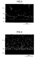
- Fig. 2 shows a cross-sectional structure of Sample No. 2 in the invention after soldering
- Fig. 3 shows a cross-sectional structure of Comparative example No. 13.
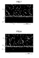
- Reference number "1" denotes a Cu substrate
- "2" denotes a Ni layer
- "3” denotes a Cu-Ni-Sn compound layer
- "4" denotes solder
- "5" denotes spalling of the compound.
- Figs. 4, 6, 8, and 10 show respective cross-sectional structures of Samples Nos. 3, 5, and 6 in the invention and of Comparative example No. 16 after soldering
- Figs. 5, 7, 9, and 11 show respective cross-sectional structures of Samples Nos. 3, 5, and 6 in the invention and of Comparative example No. 16, which were annealed at 150°C for 100 hours.
- Comparative examples Nos. 13 and 15 a thickness of the compound could not be measured since spalling of the compound 5 as shown in Fig. 3 was generated.
- a miniature Charpy impact tester was used in a evaluating method of reliability in joint, in which method a pendulum having a weight of 20 g was caused to strike against a solder bump at a speed of 1 m/s, and the probability of solder joint interfacial fracture was found. Measurement was made for 25 solder bumps. TABLE 3 indicates presence of spalling of a Cu-Ni-Sn compound at the time of soldering and results of measurement of the probability that an interface broke in impact test.
- Test substrates for the drop test were fabricated by using solder balls having a diameter of 0.3 mm to form solder bumps on BGA having 345 Ni electrodes and then using a solder paste to join the solder bumps to a mother board.
- Sn-3Ag-0.5Cu (by mass%) as generally used was used for the solder paste. Subsequently, after a test substrate was fixed horizontally to a drop table, it was dropped 30 times from a level, at which level a drop impact applied to the drop table was 1500 G to form a half-sine wave of 0.5 ms, while being maintained in a horizontal posture. In the drop test, bias of a daisy-chain circuit formed between BGA and the mother board was measured to find electrical failure. For respective compositions of solder, two test substrates, that is 30 BGAs in total, were evaluated, since 15 BGAs were mounted every test substrate.
- Times of drop corresponding to the 5% probability of failure were found from results of the test by weibull plotting the relationship between the number of cumulative failures of BGA and times of drop. TABLE 4 indicates results of times of drop corresponding to the 5% probability of failure in the drop test.
- the drop impact strength is greatly improved owing to a decrease in Ag content
- solder according to the invention is improved relative to Comparative example No. 13 in drop life by strictly controlling additions of Cu, Ag, and Ge.
- solder capable of withstanding drops of not less than 40 times is obtained by making an addition of Ge in excess of 0.01 mass% but not more than 0.06 mass%, such as Samples Nos. 3, 5, and 6 in the invention.
Landscapes
- Engineering & Computer Science (AREA)
- Chemical & Material Sciences (AREA)
- Mechanical Engineering (AREA)
- Materials Engineering (AREA)
- Metallurgy (AREA)
- Organic Chemistry (AREA)
- Manufacturing & Machinery (AREA)
- Microelectronics & Electronic Packaging (AREA)
- Electric Connection Of Electric Components To Printed Circuits (AREA)
Applications Claiming Priority (1)
| Application Number | Priority Date | Filing Date | Title |
|---|---|---|---|
| JP2005330578 | 2005-11-15 |
Publications (2)
| Publication Number | Publication Date |
|---|---|
| EP1785498A2 true EP1785498A2 (de) | 2007-05-16 |
| EP1785498A3 EP1785498A3 (de) | 2007-11-28 |
Family
ID=37837233
Family Applications (1)
| Application Number | Title | Priority Date | Filing Date |
|---|---|---|---|
| EP06023584A Withdrawn EP1785498A3 (de) | 2005-11-15 | 2006-11-13 | Lötlegierung, Lötkugel und Lötverbindung bestehend aus solcher Legierung |
Country Status (4)
| Country | Link |
|---|---|
| EP (1) | EP1785498A3 (de) |
| JP (1) | JP2007160401A (de) |
| KR (1) | KR100813574B1 (de) |
| TW (1) | TW200726567A (de) |
Cited By (1)
| Publication number | Priority date | Publication date | Assignee | Title |
|---|---|---|---|---|
| EP3315245A4 (de) * | 2015-06-29 | 2018-11-21 | Senju Metal Industry Co., Ltd | Lötmaterial, lötverbindung und verfahren zur prüfung von lötmaterial |
Families Citing this family (9)
| Publication number | Priority date | Publication date | Assignee | Title |
|---|---|---|---|---|
| CN101848787B (zh) * | 2007-08-14 | 2013-10-23 | 株式会社爱科草英 | 无铅焊料组合物及使用它的印刷电路板与电子器件 |
| CN101780608B (zh) * | 2010-04-12 | 2011-09-21 | 天津市恒固科技有限公司 | 一种含Si和Ge的SnAgCu系无铅焊料 |
| CN103028863B (zh) * | 2011-09-29 | 2016-01-20 | 郴州金箭焊料有限公司 | 一种高抗氧化无铅焊料 |
| JP6004254B2 (ja) * | 2012-05-17 | 2016-10-05 | 三菱マテリアル株式会社 | ペースト用はんだ合金粉末、ペースト及びこれを用いたはんだバンプ |
| JP6004253B2 (ja) * | 2012-05-17 | 2016-10-05 | 三菱マテリアル株式会社 | ペースト用はんだ合金粉末、ペースト及びこれを用いたはんだバンプ |
| US20150336216A1 (en) * | 2013-01-11 | 2015-11-26 | Senju Metal lndustry Co., Ltd. | Cu BALL |
| JP2016068123A (ja) * | 2014-09-30 | 2016-05-09 | 住友金属鉱山株式会社 | Au−Sn−Ag系はんだ合金及びこれを用いて封止若しくは接合された電子機器並びに該電子機器を搭載した電子装置 |
| JP6892568B2 (ja) * | 2015-12-21 | 2021-06-23 | ニホンハンダ株式会社 | 表面性に優れたSnを主成分とするはんだ合金の選別方法 |
| JP6928284B1 (ja) * | 2020-02-14 | 2021-09-01 | 千住金属工業株式会社 | 鉛フリーかつアンチモンフリーのはんだ合金、はんだボール、およびはんだ継手 |
Citations (3)
| Publication number | Priority date | Publication date | Assignee | Title |
|---|---|---|---|---|
| JPH106075A (ja) | 1996-06-13 | 1998-01-13 | Nippon Handa Kk | 無鉛ハンダ合金 |
| JPH11226776A (ja) | 1997-12-12 | 1999-08-24 | Topy Ind Ltd | 耐酸化性に優れた無鉛はんだ |
| US6179935B1 (en) | 1997-04-16 | 2001-01-30 | Fuji Electric Co., Ltd. | Solder alloys |
Family Cites Families (6)
| Publication number | Priority date | Publication date | Assignee | Title |
|---|---|---|---|---|
| JP4445046B2 (ja) * | 1998-02-06 | 2010-04-07 | 株式会社日本スペリア社 | 無鉛はんだ合金 |
| JP2000343273A (ja) * | 1999-06-01 | 2000-12-12 | Fuji Electric Co Ltd | はんだ合金 |
| JP2001071173A (ja) * | 1999-09-06 | 2001-03-21 | Ishikawa Kinzoku Kk | 無鉛はんだ |
| US6517602B2 (en) * | 2000-03-14 | 2003-02-11 | Hitachi Metals, Ltd | Solder ball and method for producing same |
| US20050100474A1 (en) * | 2003-11-06 | 2005-05-12 | Benlih Huang | Anti-tombstoning lead free alloys for surface mount reflow soldering |
| JP2005103645A (ja) * | 2004-10-29 | 2005-04-21 | Hitachi Metals Ltd | はんだボールおよびその製造方法 |
-
2006
- 2006-11-06 JP JP2006300629A patent/JP2007160401A/ja active Pending
- 2006-11-13 EP EP06023584A patent/EP1785498A3/de not_active Withdrawn
- 2006-11-14 KR KR1020060112138A patent/KR100813574B1/ko not_active Expired - Fee Related
- 2006-11-14 TW TW095141999A patent/TW200726567A/zh unknown
Patent Citations (3)
| Publication number | Priority date | Publication date | Assignee | Title |
|---|---|---|---|---|
| JPH106075A (ja) | 1996-06-13 | 1998-01-13 | Nippon Handa Kk | 無鉛ハンダ合金 |
| US6179935B1 (en) | 1997-04-16 | 2001-01-30 | Fuji Electric Co., Ltd. | Solder alloys |
| JPH11226776A (ja) | 1997-12-12 | 1999-08-24 | Topy Ind Ltd | 耐酸化性に優れた無鉛はんだ |
Cited By (2)
| Publication number | Priority date | Publication date | Assignee | Title |
|---|---|---|---|---|
| EP3315245A4 (de) * | 2015-06-29 | 2018-11-21 | Senju Metal Industry Co., Ltd | Lötmaterial, lötverbindung und verfahren zur prüfung von lötmaterial |
| US10888957B2 (en) | 2015-06-29 | 2021-01-12 | Senju Metal Industry Co., Ltd. | Soldering material |
Also Published As
| Publication number | Publication date |
|---|---|
| JP2007160401A (ja) | 2007-06-28 |
| EP1785498A3 (de) | 2007-11-28 |
| KR100813574B1 (ko) | 2008-03-17 |
| KR20070051729A (ko) | 2007-05-18 |
| TW200726567A (en) | 2007-07-16 |
Similar Documents
| Publication | Publication Date | Title |
|---|---|---|
| US9221131B2 (en) | Solder alloy | |
| US6689488B2 (en) | Lead-free solder and solder joint | |
| US9227258B2 (en) | Lead-free solder alloy having reduced shrinkage cavities | |
| KR101455966B1 (ko) | 납프리 땜납 볼 | |
| KR100833113B1 (ko) | 무연솔더합금 및 그 제조방법 | |
| EP1088615B1 (de) | Sn-Ag-Cu Lot und dessen Anwendung zur Oberfläschebehandlung und Bestückung von Bauteilen | |
| US20090197114A1 (en) | Modification of pb-free solder alloy compositions to improve interlayer dielectric delamination in silicon devices and electromigration resistance in solder joints | |
| US20090232696A1 (en) | Lead-free solder alloy | |
| US20070128068A1 (en) | Solder alloy, solder ball, and solder joint using the same | |
| US9773721B2 (en) | Lead-free solder alloy, connecting member and a method for its manufacture, and electronic part | |
| KR101345940B1 (ko) | 땜납, 납땜 방법 및 반도체 장치 | |
| EP1974850B1 (de) | Lötlegierung, lötkugel und diese verwendende lötverbindung | |
| EP1785498A2 (de) | Lötlegierung, Lötkugel und Lötverbindung bestehend aus solcher Legierung | |
| US20090197103A1 (en) | Modification of pb-free solder alloy compositions to improve interlayer dielectric delamination in silicon devices and electromigration resistance in solder joints | |
| JP3833829B2 (ja) | はんだ合金及び電子部品の実装方法 | |
| KR100904656B1 (ko) | 웨이브 및 디핑용 무연 솔더 조성물과 이를 이용한 전자기기 및 인쇄회로기판 | |
| US20040096688A1 (en) | Lead-free joining material and joining method using the same | |
| JP2005296983A (ja) | はんだ合金およびはんだボール | |
| KR20170097283A (ko) | 무연 솔더 합금 조성물 및 그의 제조 방법 |
Legal Events
| Date | Code | Title | Description |
|---|---|---|---|
| PUAI | Public reference made under article 153(3) epc to a published international application that has entered the european phase |
Free format text: ORIGINAL CODE: 0009012 |
|
| AK | Designated contracting states |
Kind code of ref document: A2 Designated state(s): AT BE BG CH CY CZ DE DK EE ES FI FR GB GR HU IE IS IT LI LT LU LV MC NL PL PT RO SE SI SK TR |
|
| AX | Request for extension of the european patent |
Extension state: AL BA HR MK YU |
|
| PUAL | Search report despatched |
Free format text: ORIGINAL CODE: 0009013 |
|
| AK | Designated contracting states |
Kind code of ref document: A3 Designated state(s): AT BE BG CH CY CZ DE DK EE ES FI FR GB GR HU IE IS IT LI LT LU LV MC NL PL PT RO SE SI SK TR |
|
| AX | Request for extension of the european patent |
Extension state: AL BA HR MK YU |
|
| 17P | Request for examination filed |
Effective date: 20080331 |
|
| 17Q | First examination report despatched |
Effective date: 20080528 |
|
| AKX | Designation fees paid |
Designated state(s): DE FI FR NL |
|
| STAA | Information on the status of an ep patent application or granted ep patent |
Free format text: STATUS: THE APPLICATION IS DEEMED TO BE WITHDRAWN |
|
| 18D | Application deemed to be withdrawn |
Effective date: 20100601 |