EP1786032A2 - Präge-Halterung die es ermöglicht Wafer einfach davon zu lösen - Google Patents
Präge-Halterung die es ermöglicht Wafer einfach davon zu lösen Download PDFInfo
- Publication number
- EP1786032A2 EP1786032A2 EP06023493A EP06023493A EP1786032A2 EP 1786032 A2 EP1786032 A2 EP 1786032A2 EP 06023493 A EP06023493 A EP 06023493A EP 06023493 A EP06023493 A EP 06023493A EP 1786032 A2 EP1786032 A2 EP 1786032A2
- Authority
- EP
- European Patent Office
- Prior art keywords
- embossing
- chuck
- wafer
- embossing part
- charge
- Prior art date
- Legal status (The legal status is an assumption and is not a legal conclusion. Google has not performed a legal analysis and makes no representation as to the accuracy of the status listed.)
- Withdrawn
Links
Images




Classifications
-
- H—ELECTRICITY
- H10—SEMICONDUCTOR DEVICES; ELECTRIC SOLID-STATE DEVICES NOT OTHERWISE PROVIDED FOR
- H10P—GENERIC PROCESSES OR APPARATUS FOR THE MANUFACTURE OR TREATMENT OF DEVICES COVERED BY CLASS H10
- H10P72/00—Handling or holding of wafers, substrates or devices during manufacture or treatment thereof
- H10P72/50—Handling or holding of wafers, substrates or devices during manufacture or treatment thereof for positioning, orientation or alignment
-
- H—ELECTRICITY
- H10—SEMICONDUCTOR DEVICES; ELECTRIC SOLID-STATE DEVICES NOT OTHERWISE PROVIDED FOR
- H10P—GENERIC PROCESSES OR APPARATUS FOR THE MANUFACTURE OR TREATMENT OF DEVICES COVERED BY CLASS H10
- H10P72/00—Handling or holding of wafers, substrates or devices during manufacture or treatment thereof
- H10P72/70—Handling or holding of wafers, substrates or devices during manufacture or treatment thereof for supporting or gripping
- H10P72/72—Handling or holding of wafers, substrates or devices during manufacture or treatment thereof for supporting or gripping using electrostatic chucks
- H10P72/722—Details of electrostatic chucks
-
- H—ELECTRICITY
- H02—GENERATION; CONVERSION OR DISTRIBUTION OF ELECTRIC POWER
- H02N—ELECTRIC MACHINES NOT OTHERWISE PROVIDED FOR
- H02N13/00—Clutches or holding devices using electrostatic attraction, e.g. using Johnson-Rahbek effect
Definitions
- the present invention relates to an embossing chuck, and more specifically, to an embossing chuck enabling a wafer to be easily detached from the chuck after putting off the plasma.
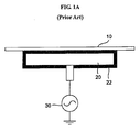
- FIGs. 1A and 1B illustrate a conventional wafer chuck 20, wherein Fig. 1A shows a detailed shape of the wafer chuck 20 and Fig. 1B shows an equivalent circuit of a case where a wafer 10 is put on the wafer chuck 20.
- a body of the wafer chuck 20 on which the wafer 10 is put on consists of aluminum and a periphery of the body is anodized and is surrounded by a dielectric layer 22 made of alumina (Al 2 O 3 ). Therefore, the wafer 10 is put on the dielectric layer 22.
- a resistance of the plasma 40 becomes infinite, so that the charges cannot flow. Accordingly, the flow of the charges as described above occurs for a short time until the plasma 40 is completely vanished. At this time, if the charges do not completely escape and remain at the wafer 10 due to surface resistances (R11, R12, R13...) of the wafer 10, the wafer 10 is not detached well from the chuck 20 due to the residual charge.
- the reference numerals C11, C12, C 13 and C 14 indicate capacitances between the chuck 20 and the wafer 10, and a reference numeral C21 indicates a capacitance between the chuck 20 and an external applying power 30.
- the charges accumulated on the wafer 10 cannot properly escape to the exterior due to a resistance (R41) of the plasma and the resistances (R11, R12, ...) of the wafer after the plasma 40 is put off, so that the wafer 10 is not detached well from the chuck 20. As a result, it is difficult to take out the wafer 10 having completed the process from a chamber.
- An object of the invention is to provide an embossing chuck having an embossing part protruding from an upper surface of a body of the chuck so as to enable charges accumulated at a wafer to easily escape to an exterior after putting off the plasma.
- an embossing chuck having an embossing part protruding, in a uniform height, from an upper surface of a body on which a wafer is put on, wherein an area of the embossing part is 5-30% for a total area of the body, viewed from the above.
- the embossing part is preferably formed along an edge of the body.
- the embossing part may be discrete and thus consist of plural segments each of which having a predetermined length.
- the embossing part consists of plural segments having an arc shape along an edge of the body.
- the embossing part preferably has a height of 0.05-0.5 mm.
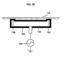
- Figs. 2A and 2B illustrate an embossing chuck 20 according to an embodiment of the invention, wherein Fig. 2A is a plan view of an embossing chuck 120 and Fig. 2B is a sectional view of a case where a wafer 110 is put on the embossing chuck 120.
- an embossing part 124 protruding, in a uniform height, from an upper surface of a body of an embossing chuck 120 is formed along an edge of the body.
- an area of the embossing part 124 is preferably 5-30% for a total area of the body.
- the embossing part 124 may consist of plural segments 124a, 124b, ... each of which having an arc shape along the edge of the body of the chuck 120.
- the invention is not limited thereto.
- the segments 124a, 124b, ... may be continuously connected to each other, thereby forming a single circle shape.
- the plasma may be formed at a back surface of the wafer 100. Accordingly, it is preferable to make the height of the embossing part 124 0.05-0.5 mm so that it is not too high.
- the body of the embossing chuck 120 consists of a metal material such as aluminum and a dielectric layer 122 such as alumina is formed at a periphery thereof.
- Fig. 3 is a circuit diagram for illustrating distribution of charges at an embossing chuck according to an embodiment of the invention.
- Q1, C1 and A1 are charge, capacitance and area of the embossing part 124 and Q2, C2 and A2 are charge, capacitance and area of a part in which the embossing part 124 is not provided.
- d1 is a vacuum thickness and d2 is a thickness of the dielectric layer 122.
- ⁇ 0 is a vacuum permittivity and ⁇ 1 is a permittivity of the dielectric layer 122.
- C2 can be assumed as a series connection of the dielectric layer 122 and a vacuum layer
- 1 C ⁇ 2 1 C dielectric layer + 1 C vacuum layer therefore
- Q1 is 93% of the overall Q and Q2 is 7% of the overall Q. This means that about 93% of the overall charge exists at the embossing part 124 and 7% of the charge exits at the part in which the embossing part is not provided.
- the area of the embossing part 124 is only 6.8% of the overall area, but the capacitance (C1/A1) per unit area of the embossing part 124 is 181 times as large as the capacitance (C2/A2) per unit area of the part in which the embossing part is not provided.
- the electrostatic force of the case where the embossing part 124 is provided is only about 7.2%, as compared to the electrostatic force of the case where the embossing part 124 is not provided as shown in Fig. 1A.
- Fig. 4 is a view for illustrating another example of an embossing chuck 120 according to an embodiment of the invention. Since only the edge of the wafer 110 is supported by the embossing part 124, a center part of the wafer 100 may be sagged down when the wafer 110 is large. Accordingly, it is preferable to additionally provide embossing parts 150 for supporting the wafer in a circle pattern.
- the electrostatic force attracting the wafer 110 becomes weak, as compared to a case where the embossing part 124 is not provided to the chuck. Therefore, it is possible to easily detach the wafer 110 from the chuck 120.
Landscapes
- Container, Conveyance, Adherence, Positioning, Of Wafer (AREA)
Applications Claiming Priority (1)
| Application Number | Priority Date | Filing Date | Title |
|---|---|---|---|
| KR1020050108585A KR100709589B1 (ko) | 2005-11-14 | 2005-11-14 | 웨이퍼를 용이하게 탈착시킬 수 있는 엠보싱 척 |
Publications (2)
| Publication Number | Publication Date |
|---|---|
| EP1786032A2 true EP1786032A2 (de) | 2007-05-16 |
| EP1786032A3 EP1786032A3 (de) | 2008-02-06 |
Family
ID=37682613
Family Applications (1)
| Application Number | Title | Priority Date | Filing Date |
|---|---|---|---|
| EP06023493A Withdrawn EP1786032A3 (de) | 2005-11-14 | 2006-11-11 | Präge-Halterung die es ermöglicht Wafer einfach davon zu lösen |
Country Status (3)
| Country | Link |
|---|---|
| US (1) | US20070109714A1 (de) |
| EP (1) | EP1786032A3 (de) |
| KR (1) | KR100709589B1 (de) |
Families Citing this family (14)
| Publication number | Priority date | Publication date | Assignee | Title |
|---|---|---|---|---|
| US8422193B2 (en) * | 2006-12-19 | 2013-04-16 | Axcelis Technologies, Inc. | Annulus clamping and backside gas cooled electrostatic chuck |
| US20080156772A1 (en) * | 2006-12-29 | 2008-07-03 | Yunsang Kim | Method and apparatus for wafer edge processing |
| US9036326B2 (en) * | 2008-04-30 | 2015-05-19 | Axcelis Technologies, Inc. | Gas bearing electrostatic chuck |
| US9558980B2 (en) * | 2008-04-30 | 2017-01-31 | Axcelis Technologies, Inc. | Vapor compression refrigeration chuck for ion implanters |
| TWI475594B (zh) | 2008-05-19 | 2015-03-01 | 恩特格林斯公司 | 靜電夾頭 |
| US8861170B2 (en) | 2009-05-15 | 2014-10-14 | Entegris, Inc. | Electrostatic chuck with photo-patternable soft protrusion contact surface |
| SG10201402319QA (en) | 2009-05-15 | 2014-07-30 | Entegris Inc | Electrostatic chuck with polymer protrusions |
| JP2013532354A (ja) | 2010-05-28 | 2013-08-15 | アクセリス テクノロジーズ, インコーポレイテッド | 冷却されるイオン注入システムのための加熱回転式のシールおよび軸受け |
| CN105196094B (zh) | 2010-05-28 | 2018-01-26 | 恩特格林斯公司 | 高表面电阻率静电吸盘 |
| US8481969B2 (en) | 2010-06-04 | 2013-07-09 | Axcelis Technologies, Inc. | Effective algorithm for warming a twist axis for cold ion implantations |
| US9711324B2 (en) | 2012-05-31 | 2017-07-18 | Axcelis Technologies, Inc. | Inert atmospheric pressure pre-chill and post-heat |
| CN103852711B (zh) * | 2012-11-30 | 2017-02-15 | 上海华虹宏力半导体制造有限公司 | 利用探针台测试晶圆的方法 |
| US9101038B2 (en) | 2013-12-20 | 2015-08-04 | Lam Research Corporation | Electrostatic chuck including declamping electrode and method of declamping |
| US10002782B2 (en) | 2014-10-17 | 2018-06-19 | Lam Research Corporation | ESC assembly including an electrically conductive gasket for uniform RF power delivery therethrough |
Citations (3)
| Publication number | Priority date | Publication date | Assignee | Title |
|---|---|---|---|---|
| WO1998057418A1 (en) | 1997-06-09 | 1998-12-17 | Applied Materials, Inc. | Cover layer for a substrate support chuck and method of fabricating same |
| US20040040665A1 (en) | 2002-06-18 | 2004-03-04 | Anelva Corporation | Electrostatic chuck device |
| WO2007005925A1 (en) | 2005-06-30 | 2007-01-11 | Varian Semiconductor Equipment Associates, Inc. | Clamp for use in processing semiconductor workpieces |
Family Cites Families (4)
| Publication number | Priority date | Publication date | Assignee | Title |
|---|---|---|---|---|
| JPH07153825A (ja) * | 1993-11-29 | 1995-06-16 | Toto Ltd | 静電チャック及びこの静電チャックを用いた被吸着体の処理方法 |
| US5583736A (en) * | 1994-11-17 | 1996-12-10 | The United States Of America As Represented By The Department Of Energy | Micromachined silicon electrostatic chuck |
| JP2003115442A (ja) * | 2001-10-04 | 2003-04-18 | Nikon Corp | 荷電粒子線露光装置におけるレチクル又はウエハの静電チャック方法 |
| KR20030067815A (ko) * | 2002-02-08 | 2003-08-19 | 삼성전자주식회사 | 온도보상기능을 갖는 노광설비용 척 |
-
2005
- 2005-11-14 KR KR1020050108585A patent/KR100709589B1/ko not_active Expired - Lifetime
-
2006
- 2006-11-11 EP EP06023493A patent/EP1786032A3/de not_active Withdrawn
- 2006-11-14 US US11/559,655 patent/US20070109714A1/en not_active Abandoned
Patent Citations (3)
| Publication number | Priority date | Publication date | Assignee | Title |
|---|---|---|---|---|
| WO1998057418A1 (en) | 1997-06-09 | 1998-12-17 | Applied Materials, Inc. | Cover layer for a substrate support chuck and method of fabricating same |
| US20040040665A1 (en) | 2002-06-18 | 2004-03-04 | Anelva Corporation | Electrostatic chuck device |
| WO2007005925A1 (en) | 2005-06-30 | 2007-01-11 | Varian Semiconductor Equipment Associates, Inc. | Clamp for use in processing semiconductor workpieces |
Also Published As
| Publication number | Publication date |
|---|---|
| EP1786032A3 (de) | 2008-02-06 |
| KR100709589B1 (ko) | 2007-04-20 |
| US20070109714A1 (en) | 2007-05-17 |
Similar Documents
| Publication | Publication Date | Title |
|---|---|---|
| EP1786032A2 (de) | Präge-Halterung die es ermöglicht Wafer einfach davon zu lösen | |
| DE10003066B4 (de) | Halbleitersensor für eine physikalische Größe und Verfahren zum Herstellen desselben | |
| DE102007060878B4 (de) | Mikromechanisches System | |
| US8039922B2 (en) | Variable capacitor employing MEMS technology | |
| EP2474372A2 (de) | Superhydrophobe Mikrostruktur | |
| US20010019029A1 (en) | Micromachined membrane particle filter using parylene reinforcement | |
| EP1022783A3 (de) | Integrierte Schaltungsvorrichtung mit einer Doppel-Damascene-Kondensator und deren Herstellungsverfahren | |
| EP1398811B1 (de) | Geschaltete Kapazität | |
| WO1998033032B1 (en) | Method for preparing hollow microchannels and product | |
| FI127231B (fi) | Mikrosähkömekaaninen kytkinkokoonpano ja menetelmä mikrosähkömekaanisen kytkinkokoonpanon valmistamiseksi | |
| EP0928959A3 (de) | Variabler Halbleiterkondensator und Herstellungsverfahren | |
| EP2202783A3 (de) | Kondensator und Verfahren zu dessen Herstellung | |
| EP0924077A3 (de) | Als Teil eines Heizelementes zum Beseitigen von Flüssigkeitsverunreinigungen ausgebildetes Filter und Verfahren zum Herstellen desselben | |
| WO2005117085A3 (en) | Gap-type conductive interconnect structures in semiconductor device | |
| EP0924078A3 (de) | Zum Beseitigen von Flüssigkeitsverunreinigungen Filter und Verfahren zum Herstellen desselben | |
| JP4737440B2 (ja) | チップ状電子部品用冶具 | |
| EP1005077A3 (de) | Substratträgervorrichtung und Verfahren zu ihrer Herstellung | |
| EP0849789A3 (de) | Methode zum Ätzen einer mehrschichtigen Dielektrikumsstruktur eines ICs | |
| EP1018699A3 (de) | Topographisches Gitter zur elektrostatischen Beschützung von Sensoren | |
| DE19735155A1 (de) | Beschleunigungssensor | |
| CN108373135A (zh) | 包括体积减少的压电致动器的mems设备 | |
| EP1156522A3 (de) | Elektrostatischer Scheibenhalter mit einer isolierenden Schicht | |
| DE10141867B4 (de) | Halbleitersensor für dynamische Grössen mit beweglichen Elektroden und Festelektroden auf einem Unterstützungssubstrat | |
| EP1286187A3 (de) | Optische Vorrichtung zur Filterung und Detektierung | |
| WO2007038778A3 (en) | Ballast circuit for electrostastic particle collection systems |
Legal Events
| Date | Code | Title | Description |
|---|---|---|---|
| PUAI | Public reference made under article 153(3) epc to a published international application that has entered the european phase |
Free format text: ORIGINAL CODE: 0009012 |
|
| AK | Designated contracting states |
Kind code of ref document: A2 Designated state(s): AT BE BG CH CY CZ DE DK EE ES FI FR GB GR HU IE IS IT LI LT LU LV MC NL PL PT RO SE SI SK TR |
|
| AX | Request for extension of the european patent |
Extension state: AL BA HR MK YU |
|
| PUAL | Search report despatched |
Free format text: ORIGINAL CODE: 0009013 |
|
| AK | Designated contracting states |
Kind code of ref document: A3 Designated state(s): AT BE BG CH CY CZ DE DK EE ES FI FR GB GR HU IE IS IT LI LT LU LV MC NL PL PT RO SE SI SK TR |
|
| AX | Request for extension of the european patent |
Extension state: AL BA HR MK YU |
|
| 17P | Request for examination filed |
Effective date: 20080804 |
|
| 17Q | First examination report despatched |
Effective date: 20080909 |
|
| AKX | Designation fees paid |
Designated state(s): DE FR IT |
|
| STAA | Information on the status of an ep patent application or granted ep patent |
Free format text: STATUS: THE APPLICATION IS DEEMED TO BE WITHDRAWN |
|
| 18D | Application deemed to be withdrawn |
Effective date: 20100601 |