EP1786046A2 - Nichtflüchtige Speichervorrichtung und deren Herstellungsverfahren - Google Patents
Nichtflüchtige Speichervorrichtung und deren Herstellungsverfahren Download PDFInfo
- Publication number
- EP1786046A2 EP1786046A2 EP06123835A EP06123835A EP1786046A2 EP 1786046 A2 EP1786046 A2 EP 1786046A2 EP 06123835 A EP06123835 A EP 06123835A EP 06123835 A EP06123835 A EP 06123835A EP 1786046 A2 EP1786046 A2 EP 1786046A2
- Authority
- EP
- European Patent Office
- Prior art keywords
- electrode
- data storage
- layer
- contact layer
- volatile memory
- Prior art date
- Legal status (The legal status is an assumption and is not a legal conclusion. Google has not performed a legal analysis and makes no representation as to the accuracy of the status listed.)
- Granted
Links
Images


Classifications
-
- H—ELECTRICITY
- H10—SEMICONDUCTOR DEVICES; ELECTRIC SOLID-STATE DEVICES NOT OTHERWISE PROVIDED FOR
- H10B—ELECTRONIC MEMORY DEVICES
- H10B63/00—Resistance change memory devices, e.g. resistive RAM [ReRAM] devices
- H10B63/30—Resistance change memory devices, e.g. resistive RAM [ReRAM] devices comprising selection components having three or more electrodes, e.g. transistors
-
- H—ELECTRICITY
- H10—SEMICONDUCTOR DEVICES; ELECTRIC SOLID-STATE DEVICES NOT OTHERWISE PROVIDED FOR
- H10N—ELECTRIC SOLID-STATE DEVICES NOT OTHERWISE PROVIDED FOR
- H10N70/00—Solid-state devices having no potential barriers, and specially adapted for rectifying, amplifying, oscillating or switching
- H10N70/20—Multistable switching devices, e.g. memristors
-
- H—ELECTRICITY
- H10—SEMICONDUCTOR DEVICES; ELECTRIC SOLID-STATE DEVICES NOT OTHERWISE PROVIDED FOR
- H10N—ELECTRIC SOLID-STATE DEVICES NOT OTHERWISE PROVIDED FOR
- H10N70/00—Solid-state devices having no potential barriers, and specially adapted for rectifying, amplifying, oscillating or switching
- H10N70/801—Constructional details of multistable switching devices
- H10N70/821—Device geometry
- H10N70/826—Device geometry adapted for essentially vertical current flow, e.g. sandwich or pillar type devices
-
- H—ELECTRICITY
- H10—SEMICONDUCTOR DEVICES; ELECTRIC SOLID-STATE DEVICES NOT OTHERWISE PROVIDED FOR
- H10N—ELECTRIC SOLID-STATE DEVICES NOT OTHERWISE PROVIDED FOR
- H10N70/00—Solid-state devices having no potential barriers, and specially adapted for rectifying, amplifying, oscillating or switching
- H10N70/801—Constructional details of multistable switching devices
- H10N70/841—Electrodes
-
- H—ELECTRICITY
- H10—SEMICONDUCTOR DEVICES; ELECTRIC SOLID-STATE DEVICES NOT OTHERWISE PROVIDED FOR
- H10N—ELECTRIC SOLID-STATE DEVICES NOT OTHERWISE PROVIDED FOR
- H10N70/00—Solid-state devices having no potential barriers, and specially adapted for rectifying, amplifying, oscillating or switching
- H10N70/801—Constructional details of multistable switching devices
- H10N70/881—Switching materials
- H10N70/882—Compounds of sulfur, selenium or tellurium, e.g. chalcogenides
- H10N70/8825—Selenides, e.g. GeSe
-
- H—ELECTRICITY
- H10—SEMICONDUCTOR DEVICES; ELECTRIC SOLID-STATE DEVICES NOT OTHERWISE PROVIDED FOR
- H10N—ELECTRIC SOLID-STATE DEVICES NOT OTHERWISE PROVIDED FOR
- H10N70/00—Solid-state devices having no potential barriers, and specially adapted for rectifying, amplifying, oscillating or switching
- H10N70/801—Constructional details of multistable switching devices
- H10N70/881—Switching materials
- H10N70/882—Compounds of sulfur, selenium or tellurium, e.g. chalcogenides
- H10N70/8828—Tellurides, e.g. GeSbTe
-
- H—ELECTRICITY
- H10—SEMICONDUCTOR DEVICES; ELECTRIC SOLID-STATE DEVICES NOT OTHERWISE PROVIDED FOR
- H10N—ELECTRIC SOLID-STATE DEVICES NOT OTHERWISE PROVIDED FOR
- H10N70/00—Solid-state devices having no potential barriers, and specially adapted for rectifying, amplifying, oscillating or switching
- H10N70/801—Constructional details of multistable switching devices
- H10N70/881—Switching materials
- H10N70/883—Oxides or nitrides
- H10N70/8833—Binary metal oxides, e.g. TaOx
Definitions
- the present invention relates to a non-volatile memory device using a resistance material, and more particularly, to a non-volatile memory device with an improved structure to have a stable memory switching characteristic in a storage node and a fabrication method thereof.
- Ferroelectric random access memory FRAM
- magnetoresistive RAM MRAM
- phase-change RAM PRAM
- DRAM dynamic RAM
- FRAM, MRAM and PRAM store binary information using a polarization characteristic of a ferroelectric material, a resistance change of a magnetic tunnel junction (MTJ) according to a magnetized state of a strong magnetic material, and a resistance change due to a phase change, respectively.
- MTJ magnetic tunnel junction
- these FRAM, MRAM and PRAM can be integrated in large scale as like DRAM and are also non-volatile as like flash memories.
- FRAM, MRAM and PRAM have been highlighted as potential memories which can replace conventional volatile or non-volatile memories.
- PRAM retrieves binary information using a certain characteristic of a phase-change material such as GeSbTe (GST).
- GST GeSbTe
- This exemplified phase-change material changes its phase into a crystalline or amorphous state by heat generated regionally when an electric pulse is applied to the phase-change material.
- a memory cell which stores binary information includes a phase-change layer, a resistor and a switch transistor.
- the phase-change layer is a GST-based material and is often called chalcogenide.
- the resistor is used to heat the phase-change layer.
- a resistance value varies since the phase-change layer changes its phase into a crystalline or amorphous state. Also, current flowing into the resistor causes a voltage level to vary, and this variable voltage level makes it possible for PRAM to store and read binary information.
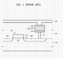
- FIG. 1 is a cross-sectional view briefly illustrating a conventional non-volatile memory device.
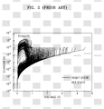
- FIG. 2 is a graph illustrating a switching characteristic of a storage node illustrated in FIG. 1.
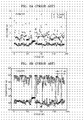
- FIG. 3A is a graph illustrating a distribution of set and reset voltage values applied to the storage node illustrated in FIG. 1.
- FIG. 3B is a graph illustrating a distribution of resistance values of the storage node depending on an on or off state.
- the conventional non-volatile memory device using a thin NiO layer includes a transistor 20 and a storage node 28 coupled with the transistor 20.
- the transistor 20 includes a source 12S, a drain 12D, a channel 12C, and a gate electrode 14.
- the storage node 28 includes an upper electrode 26, a lower electrode 24, and a thin NiO layer 25 disposed therebetween.
- An insulation layer 30 is disposed between the storage node 28 and the transistor 20.
- the storage node 28 is coupled with the transistor 20 through a conductive contact plug 22, and a plate electrode 32 is formed over the upper electrode 27.
- the storage node 28 of the conventional non-volatile memory device has an M-I-M memory cell structure.
- 'M' represents metal-based upper and lower electrodes
- 'I' represents a NiO layer, which is a resistance material.
- set voltage values V set and reset voltage values V reset applied to a storage node during repetitive switchings may be distributed with a large deviation.
- the storage node may have non-uniform resistance values R on and R off depending on an on or off state.
- the conventional storage node structure needs to be improved.
- a non-volatile memory device including: a switching device; and a storage node coupled with the switching device, the storage node including: a first electrode; a second electrode; a data storage layer disposed between the first electrode and the second electrode and including a transition metal oxide or aluminum oxide; and at least one contact layer disposed beneath or above the data storage layer and including a conductive metal oxide to improve interfacial characteristics between the data storage layer and the first electrode and between the data storage layer and the second electrode.
- the conductive metal oxide may be one selected from the group consisting of IrO 2 , RuO 2 , SrRuO 3 , MoO 2 , OsO 2 , ReO 2 , RhO 2 , WO 2 , and indium tin oxide (ITO).
- the at least one contact layer may have a thickness ranging from approximately 10 ⁇ to approximately 500 ⁇ .
- the transition metal oxide may be an oxide of a metal selected from the group consisting of Ni, Nb, Ti, Zr, Hf, Co, Fe, Cu, and Cr.
- Each of the first electrode and the second electrode may be formed of a material selected from the group consisting of Ir, Pt, Ru, W, TiN, and polysilicon.
- the switching device may be a transistor or a diode.
- a method of fabricating a non-volatile memory device including: preparing a switching device; forming a first electrode coupled with the switching device; forming a first contact layer over the first electrode, the first contact layer including a conductive metal oxide; forming a data storage layer formed over the first contact layer, the data storage layer including a transition metal oxide or aluminum oxide; and forming a second electrode over the data storage layer.
- the above method may further include forming a second contact layer on the data storage layer using a conductive metal oxide between the forming of the data storage layer and the forming of the second electrode.
- a method of fabricating a non-volatile memory device including: preparing a switching device; forming a first electrode coupled with the switching device; forming a data storage layer formed over the first electrode, the data storage layer including a transition metal oxide or aluminum oxide; forming a contact layer over the data storage layer, the contact layer including a conductive metal oxide; and forming a second electrode over the contact layer.
- the conductive metal oxide may be one selected from the group consisting of IrO 2 , RuO 2 , SrRuO 3 , MoO 2 , OsO 2 , ReO 2 , RhO 2 , WO 2 , and ITO (indium tin oxide).
- the contact layer may be formed to a thickness ranging from approximately 10 ⁇ to approximately 500 ⁇ .
- the transition metal oxide may be an oxide of a metal selected from the group consisting of Ni, Nb, Ti, Zr, Hf, Co, Fe, Cu, and Cr.
- Each of the first electrode and the second electrode may be formed of a material selected from the group consisting of Ir, Pt, Ru, W, TiN, and polysilicon.
- the switching device may be a transistor or a diode.
- the present invention aims to provide a non-volatile memory device with an improved structure to have a stable memory switching characteristic in a storage node and a fabrication method thereof.
- the non-volatile memory device is implemented with an improved structure, which provides a stable switching characteristic in the storage node.
- FIG. 4 is a cross-sectional view briefly illustrating a non-volatile memory device according to an embodiment of the present invention.
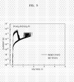
- FIG. 5 is a graph illustrating a switching characteristic of a storage node illustrated in FIG. 4.
- the non-volatile memory device includes a transistor 120 and a storage node 128.
- the transistor 120 is a switching device, and the storage node 128 is coupled with the transistor 120.
- An insulation layer 130 is disposed between the storage node 128 and the transistor 120, and a conductive contact plug 122 couples the storage node 128 with the transistor 120.
- a plate electrode 132 is disposed over the storage node 128 and coupled with the storage node 128.
- the transistor 120 includes a source 112S, a drain 112D, a channel 112C, and a gate electrode 114. Since a structure of the transistor 120 and a fabrication method thereof are well known in the art, detailed description thereof will be omitted.
- transistor 120 instead of the transistor 120, other switching devices, e.g., diodes, can be used.
- a diode structure and a fabrication method thereof are also well known in the art, detailed description thereof will be omitted.
- the exemplary embodiment of the present invention will be described in detail on the basis of the transistor.
- the storage node 128 includes a first electrode 123, a second electrode 127, a data storage layer 125 disposed between the first electrode 123 and the second electrode 127, and first and second contact layers 124 and 126 disposed at least beneath or above the data storage layer 125.
- the data storage layer 125 becomes a reset state or a set state depending on a voltage level applied to the data storage layer 125 (refer to FIG. 5). Since the data storage layer 125 has different resistance values for each state, binary information can be stored and read based on a difference between the resistance values.
- the data storage layer 125 can include a transition metal oxide or aluminum oxide.
- the transition metal oxide is an oxide of a metal selected from the group consisting of nickel (Ni), niobium (Nb), titanium (Ti), zirconium (Zr), hafnium (Hf), cobalt (Co), iron (Fe), copper (Cu), and chrome (Cr).
- the first electrode 123 and the second electrode 127 includes one selected from the group consisting of iridium (Ir), platinum (Pt), ruthenium (Ru), tungsten (W), titanium nitride (TiN), and polysilicon.
- the first and second contact layers 124 and 126 include a conductive metal oxide, and because the first and second contact layers 124 and 126 are formed at least beneath or above the data storage layer 125, the first and second contact layers 124 and 126 can improve interfacial characteristics between the data storage layer 125 and the lower electrode 123 and between the upper electrode 127 and the data storage layer 125.
- the conductive metal oxide is one selected from the group consisting of IrO 2 , RuO 2 , SrRuO 3 , MoO 2 , OsO 2 , ReO 2 , RhO 2 , WO 2 , and indium tin oxide (ITO).
- the first and second contact layers 124 and 126 have a thickness ranging from approximately 10 ⁇ to approximately 500 ⁇ .
- the storage node 128 of the non-volatile memory device can have an M-B-I-B-M, M-B-I-M or M-I-B-M memory cell structure.
- 'M' represents the first electrode 123 and the second electrode 127 both including a metal or conductive material.
- 'I' and 'B' represent the data storage layer 125 and the first and second contact layers 124 and 126, respectively.
- the conventional resistance material based memory device with the M-I-M memory cell structure often has limitations in that set and reset voltage values Vset and Vreset applied to the storage node during repetitive switchings are distributed with a large deviation and resistance values Ron and Roff of the storage node depending on an on or off state are not distributed uniformly.
- these limitations can be improved by improving the interfacial characteristics between the data storage layer 125 and the first electrode 123 and between the data storage layer 125 and the upper electrode 127.
- the resistance values of the storage node 128 can be distributed with a decreased level of deviation due to the improved interfacial characteristics as compared with the conventional resistance material based memory device. Therefore, the storage node 128 can have a stable memory switching characteristic.
- FIGS. 6A through 7B illustrate an improved memory switching characteristic in the non-volatile memory device according to the embodiment of the present invention.
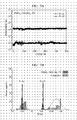
- FIG. 6A is a graph illustrating a distribution of set and reset voltage values applied to the storage node illustrated in FIG. 4, and FIG. 6B is a histogram of the set and reset voltage values illustrated in FIG. 6A.
- FIG. 7A is a graph illustrating a distribution of resistance values of the storage node depending on an on or off state, and FIG. 7B is a histogram of the resistance values of the storage node illustrated in FIG. 7A.
- the storage node 128 has the set and reset voltage values Vset and Vreset with decreased standard deviations.
- Table 1 below exhibits data obtained from measuring set and reset voltage values Vset and Vreset of the conventional M-I-M memory cell structure and the M-B-I-B-M memory cell structure and then comparing average values, standard deviation values, maximum values and minimum values of the measured set voltage values Vset and the reset voltage values Vreset with each other.
- the set voltage values Vset and the reset voltage values Vreset are measured in voltages.
- the storage node 128 has the resistance values Ron and Roff with decreased standard deviations.
- Table 2 exhibits data obtained from measuring resistance values Ron and Roff of the conventional M-I-M memory cell structure and the M-B-I-B-M memory cell structure and then comparing average values, standard deviation values, maximum values and minimum values of the measured resistance values Ron and Roff with each other.
- the resistance values Ron and Roff are measured in ohms.
- Table 3 below exhibits data for a detailed structure of the storage node used in measuring the set and reset voltage values Vset and Vreset and the resistance values Ron and Roff and various sputtering deposition conditions for depositing an IrO 2 contact layer.
- Table 3 Sample Structure NiO thickness IrO 2 thickness Sputter process 1.
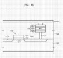
- FIGS. 8A through 8E are cross-sectional views illustrating a method of fabricating a non-volatile memory device according to an embodiment of the present invention.
- a typical vacuum deposition method such as a chemical vapor deposition (CVD) method or a physical vapor deposition (PVD) method can be used to deposit target layers.
- the PVD method includes a sputtering method.
- the non-volatile memory device according to the present embodiment includes a transistor 120, which is a switching device, and a storage node 128 coupled with the transistor 120. Instead of the transistor 120, other switching devices such as diodes can also be used. Since a diode structure and a fabrication method thereof are well known in the art, detailed description thereof will be omitted.
- the present embodiment on a fabrication method of such a non-volatile memory device will be described in detail on the basis of the transistor.
- the transistor 120 which includes a source 112S, a drain 112D, a channel 112C, and a gate electrode 114, is provided.
- An insulation layer 130 is formed over the transistor 120. Since a structure of the transistor 120 and a fabrication method thereof are well known in the art, detailed description thereof will be omitted.
- a contact hole is formed in the insulation layer 130.
- the contact hole exposes the source 112S or the drain 112D.
- a conductive material is then filled into the contact hole to form a contact plug 122.
- a first electrode 123 is formed over a portion of the insulation layer 130 such that the first electrode 123 contacts the contact plug 122.
- the first electrode 123 includes one selected from the group consisting of Ir, Pt, Ru, W, TiN, and polysilicon.
- a first contact layer 124 is formed over the first electrode 123.
- the first contact layer 124 includes a conductive metal oxide selected from the group consisting of IrO 2 , RuO 2 , SrRuO 3 , MoO 2 , OsO 2 , ReO 2 , RhO 2 , WO 2 , and ITO.
- the first contact layer 124 has a thickness of approximately 10 ⁇ to approximately 500 ⁇ .
- a data storage layer 125 is formed over the first contact layer 124.
- the data storage layer 125 includes a transition metal oxide or aluminum oxide.
- the transition metal oxide is an oxide of a metal selected from the group consisting of Ni, Nb, Ti, Zr, Hf, Co, Fe, Cu, and Cr.
- a second contact layer 126 is formed over the data storage layer 125.
- the second contact layer 126 includes a transition metal oxide selected from the group consisting of IrO 2 , RuO 2 , SrRuO 3 , MoO 2 , OsO 2 , ReO 2 , RhO 2 , WO 2 , and ITO.
- the second contact layer 126 has a thickness of approximately 10 ⁇ to approximately 500 ⁇ .
- a second electrode 127 is formed over the second contact layer 126.
- the second electrode 127 is one selected from the group consisting of Ir, Pt, Ru, W, TiN, and polysilicon.
- the insulation layer 130 is formed again over the above resultant structure (refer to FIG. 8D) until the insulation layer 130 buries the storage node 128.
- the non-volatile memory device can have a stable memory switching characteristic in the storage node.
- Using the contact layer formed of a conductive metal oxide such as IrO 2 can improve the interfacial characteristics between the data storage layer and the first electrode and between the data storage layer and the second electrode.
- the improved interfacial characteristics can decrease a deviation of resistance values of the storage node depending on an on or off state, and also a deviation of set and reset voltage values applied to the storage node. Accordingly, a stable memory switching characteristic can be obtained.
Landscapes
- Semiconductor Memories (AREA)
Applications Claiming Priority (1)
| Application Number | Priority Date | Filing Date | Title |
|---|---|---|---|
| KR1020050108125A KR100668348B1 (ko) | 2005-11-11 | 2005-11-11 | 비휘발성 메모리 소자 및 그 제조방법 |
Publications (3)
| Publication Number | Publication Date |
|---|---|
| EP1786046A2 true EP1786046A2 (de) | 2007-05-16 |
| EP1786046A3 EP1786046A3 (de) | 2008-03-26 |
| EP1786046B1 EP1786046B1 (de) | 2012-02-08 |
Family
ID=37672457
Family Applications (1)
| Application Number | Title | Priority Date | Filing Date |
|---|---|---|---|
| EP06123835A Active EP1786046B1 (de) | 2005-11-11 | 2006-11-10 | Nichtflüchtige Speichervorrichtung und deren Herstellungsverfahren |
Country Status (5)
| Country | Link |
|---|---|
| US (1) | US7936044B2 (de) |
| EP (1) | EP1786046B1 (de) |
| JP (1) | JP2007134724A (de) |
| KR (1) | KR100668348B1 (de) |
| CN (1) | CN1964050B (de) |
Cited By (3)
| Publication number | Priority date | Publication date | Assignee | Title |
|---|---|---|---|---|
| EP2239795A1 (de) * | 2009-04-10 | 2010-10-13 | Imec | Verfahren zur Herstellung eines Speicherelements mit widerstandsschaltender NiO-Schicht und daraus erhaltene Vorrichtungen |
| WO2010115924A1 (en) * | 2009-04-10 | 2010-10-14 | Imec | METHOD FOR MANUFACTURING A MEMORY ELEMENT COMPRISING A RESISTIVITY-SWITCHING NiO LAYER AND DEVICES OBTAINED THEREOF |
| WO2018037204A1 (en) * | 2016-08-22 | 2018-03-01 | Arm Ltd | A cem switching device |
Families Citing this family (26)
| Publication number | Priority date | Publication date | Assignee | Title |
|---|---|---|---|---|
| US8003511B2 (en) * | 2008-12-19 | 2011-08-23 | Unity Semiconductor Corporation | Memory cell formation using ion implant isolated conductive metal oxide |
| KR101239962B1 (ko) * | 2006-05-04 | 2013-03-06 | 삼성전자주식회사 | 하부 전극 상에 형성된 버퍼층을 포함하는 가변 저항메모리 소자 |
| KR101206036B1 (ko) * | 2006-11-16 | 2012-11-28 | 삼성전자주식회사 | 전이 금속 고용체를 포함하는 저항성 메모리 소자 및 그제조 방법 |
| KR100898897B1 (ko) | 2007-02-16 | 2009-05-27 | 삼성전자주식회사 | 비휘발성 메모리 소자 및 그 형성방법 |
| US20080273370A1 (en) * | 2007-05-02 | 2008-11-06 | Jan Keller | Integrated Circuit, Method of Operating an Integrated Circuit, Memory Cell Array, and Memory Module |
| US7549695B2 (en) * | 2007-05-24 | 2009-06-23 | Royer Real | Device for manipulating a tarpaulin |
| US8173989B2 (en) * | 2007-05-30 | 2012-05-08 | Samsung Electronics Co., Ltd. | Resistive random access memory device and methods of manufacturing and operating the same |
| TWI402980B (zh) * | 2007-07-20 | 2013-07-21 | Macronix Int Co Ltd | 具有緩衝層之電阻式記憶結構 |
| US8154003B2 (en) | 2007-08-09 | 2012-04-10 | Taiwan Semiconductor Manufacturing Company, Ltd. | Resistive non-volatile memory device |
| KR101326077B1 (ko) | 2007-08-24 | 2013-11-07 | 삼성전자주식회사 | 저항성 메모리 소자 |
| US7652502B2 (en) * | 2007-12-29 | 2010-01-26 | Unity Semiconductor Corporation | Field programmable gate arrays using resistivity sensitive memories |
| WO2009125777A1 (ja) * | 2008-04-07 | 2009-10-15 | 日本電気株式会社 | 抵抗変化素子及びその製造方法 |
| CN101329701B (zh) * | 2008-07-09 | 2010-06-09 | 清华大学 | 一种应用于CeRAM的TMO材料 |
| WO2010029645A1 (ja) * | 2008-09-12 | 2010-03-18 | 株式会社 東芝 | 不揮発性記憶装置及びその製造方法 |
| US8519376B2 (en) * | 2008-10-27 | 2013-08-27 | Seagate Technology Llc | Nonvolatile resistive memory devices |
| KR101004736B1 (ko) | 2009-07-17 | 2011-01-04 | 재단법인대구경북과학기술원 | 비휘발성 저항 메모리소자 및 이의 제조방법 |
| TWI478161B (zh) * | 2010-01-19 | 2015-03-21 | Macronix Int Co Ltd | 具有場增強排列的記憶體裝置 |
| JP5270044B2 (ja) * | 2010-10-01 | 2013-08-21 | パナソニック株式会社 | 不揮発性記憶素子の製造方法および不揮発性記憶素子 |
| JP5674548B2 (ja) * | 2011-04-28 | 2015-02-25 | 株式会社日立製作所 | 半導体記憶装置 |
| CN104078562B (zh) * | 2013-03-25 | 2016-12-28 | 华邦电子股份有限公司 | 电阻式非挥发性内存装置 |
| US9112148B2 (en) * | 2013-09-30 | 2015-08-18 | Taiwan Semiconductor Manufacturing Co., Ltd. | RRAM cell structure with laterally offset BEVA/TEVA |
| US9012878B1 (en) * | 2013-12-23 | 2015-04-21 | Intermolecular, Inc. | MoOx based selector element |
| US9178144B1 (en) | 2014-04-14 | 2015-11-03 | Taiwan Semiconductor Manufacturing Co., Ltd. | RRAM cell with bottom electrode |
| US10611161B2 (en) | 2014-07-24 | 2020-04-07 | Avision Inc. | Image forming agent storage member and laser printer using the same |
| US9209392B1 (en) | 2014-10-14 | 2015-12-08 | Taiwan Semiconductor Manufacturing Co., Ltd. | RRAM cell with bottom electrode |
| TWI559519B (zh) * | 2015-02-16 | 2016-11-21 | 國立清華大學 | 電阻式記憶體 |
Family Cites Families (14)
| Publication number | Priority date | Publication date | Assignee | Title |
|---|---|---|---|---|
| JP3388089B2 (ja) * | 1996-04-25 | 2003-03-17 | シャープ株式会社 | 不揮発性半導体メモリ素子の製造方法 |
| US5825046A (en) * | 1996-10-28 | 1998-10-20 | Energy Conversion Devices, Inc. | Composite memory material comprising a mixture of phase-change memory material and dielectric material |
| KR100343287B1 (ko) * | 1999-09-21 | 2002-07-15 | 윤종용 | 고집적 강유전체 메모리 소자의 형성 방법 |
| KR100351451B1 (ko) * | 1999-12-30 | 2002-09-09 | 주식회사 하이닉스반도체 | 반도체메모리장치의 커패시터제조방법 |
| KR100395766B1 (ko) * | 2001-02-12 | 2003-08-25 | 삼성전자주식회사 | 강유전체 기억 소자 및 그 형성 방법 |
| US6635497B2 (en) * | 2001-12-21 | 2003-10-21 | Texas Instruments Incorporated | Methods of preventing reduction of IrOx during PZT formation by metalorganic chemical vapor deposition or other processing |
| US7067862B2 (en) * | 2002-08-02 | 2006-06-27 | Unity Semiconductor Corporation | Conductive memory device with conductive oxide electrodes |
| KR100773537B1 (ko) | 2003-06-03 | 2007-11-07 | 삼성전자주식회사 | 한 개의 스위칭 소자와 한 개의 저항체를 포함하는비휘발성 메모리 장치 및 그 제조 방법 |
| US7259039B2 (en) * | 2003-07-09 | 2007-08-21 | Spansion Llc | Memory device and methods of using and making the device |
| US7029924B2 (en) * | 2003-09-05 | 2006-04-18 | Sharp Laboratories Of America, Inc. | Buffered-layer memory cell |
| US6849891B1 (en) * | 2003-12-08 | 2005-02-01 | Sharp Laboratories Of America, Inc. | RRAM memory cell electrodes |
| CN1938781B (zh) * | 2004-04-16 | 2011-09-21 | 松下电器产业株式会社 | 具有可变电阻的薄膜存储器件 |
| KR101051704B1 (ko) * | 2004-04-28 | 2011-07-25 | 삼성전자주식회사 | 저항 구배를 지닌 다층막을 이용한 메모리 소자 |
| KR100576369B1 (ko) * | 2004-11-23 | 2006-05-03 | 삼성전자주식회사 | 전이 금속 산화막을 데이타 저장 물질막으로 채택하는비휘발성 기억소자의 프로그램 방법 |
-
2005
- 2005-11-11 KR KR1020050108125A patent/KR100668348B1/ko not_active Expired - Fee Related
-
2006
- 2006-04-10 CN CN2006100753459A patent/CN1964050B/zh not_active Expired - Fee Related
- 2006-04-14 US US11/403,902 patent/US7936044B2/en not_active Expired - Fee Related
- 2006-11-10 JP JP2006305634A patent/JP2007134724A/ja active Pending
- 2006-11-10 EP EP06123835A patent/EP1786046B1/de active Active
Cited By (4)
| Publication number | Priority date | Publication date | Assignee | Title |
|---|---|---|---|---|
| EP2239795A1 (de) * | 2009-04-10 | 2010-10-13 | Imec | Verfahren zur Herstellung eines Speicherelements mit widerstandsschaltender NiO-Schicht und daraus erhaltene Vorrichtungen |
| WO2010115924A1 (en) * | 2009-04-10 | 2010-10-14 | Imec | METHOD FOR MANUFACTURING A MEMORY ELEMENT COMPRISING A RESISTIVITY-SWITCHING NiO LAYER AND DEVICES OBTAINED THEREOF |
| WO2018037204A1 (en) * | 2016-08-22 | 2018-03-01 | Arm Ltd | A cem switching device |
| US10586924B2 (en) | 2016-08-22 | 2020-03-10 | Arm Ltd. | CEM switching device |
Also Published As
| Publication number | Publication date |
|---|---|
| EP1786046B1 (de) | 2012-02-08 |
| KR100668348B1 (ko) | 2007-01-12 |
| CN1964050A (zh) | 2007-05-16 |
| CN1964050B (zh) | 2011-05-04 |
| US20070120580A1 (en) | 2007-05-31 |
| JP2007134724A (ja) | 2007-05-31 |
| EP1786046A3 (de) | 2008-03-26 |
| US7936044B2 (en) | 2011-05-03 |
Similar Documents
| Publication | Publication Date | Title |
|---|---|---|
| EP1786046B1 (de) | Nichtflüchtige Speichervorrichtung und deren Herstellungsverfahren | |
| US20230121892A1 (en) | Ferroelectric Capacitor, Ferroelectric Field Effect Transistor, and Method Used in Forming an Electronic Component Comprising Conductive Material and Ferroelectric Material | |
| US8441838B2 (en) | Resistive-switching nonvolatile memory elements | |
| US8318573B2 (en) | Nonvolatile memory elements | |
| US8154003B2 (en) | Resistive non-volatile memory device | |
| US8525142B2 (en) | Non-volatile variable resistance memory device and method of fabricating the same | |
| KR100682926B1 (ko) | 저항체를 이용한 비휘발성 메모리 소자 및 그 제조방법 | |
| US8502184B2 (en) | Nonvolatile memory device using variable resistive element | |
| US9159914B2 (en) | Nonvolatile memory devices and methods of forming the same | |
| US9019744B2 (en) | Barrier design for steering elements |
Legal Events
| Date | Code | Title | Description |
|---|---|---|---|
| PUAI | Public reference made under article 153(3) epc to a published international application that has entered the european phase |
Free format text: ORIGINAL CODE: 0009012 |
|
| AK | Designated contracting states |
Kind code of ref document: A2 Designated state(s): AT BE BG CH CY CZ DE DK EE ES FI FR GB GR HU IE IS IT LI LT LU LV MC NL PL PT RO SE SI SK TR |
|
| AX | Request for extension of the european patent |
Extension state: AL BA HR MK YU |
|
| PUAL | Search report despatched |
Free format text: ORIGINAL CODE: 0009013 |
|
| AK | Designated contracting states |
Kind code of ref document: A3 Designated state(s): AT BE BG CH CY CZ DE DK EE ES FI FR GB GR HU IE IS IT LI LT LU LV MC NL PL PT RO SE SI SK TR |
|
| AX | Request for extension of the european patent |
Extension state: AL BA HR MK YU |
|
| 17P | Request for examination filed |
Effective date: 20080903 |
|
| 17Q | First examination report despatched |
Effective date: 20081002 |
|
| AKX | Designation fees paid |
Designated state(s): DE FR GB |
|
| GRAP | Despatch of communication of intention to grant a patent |
Free format text: ORIGINAL CODE: EPIDOSNIGR1 |
|
| RIN1 | Information on inventor provided before grant (corrected) |
Inventor name: YOO, IN-KYEONG Inventor name: AHN, SEUNG-EON Inventor name: CHA, YOUNG-KWAN Inventor name: LEE, MYOUNG-JAE Inventor name: PARK, SANG-JIN Inventor name: BAEK, IN-GYU Inventor name: SEO, SUN-AE Inventor name: KIM, DONG-CHUL Inventor name: PARK, BYOUNG-HO |
|
| GRAS | Grant fee paid |
Free format text: ORIGINAL CODE: EPIDOSNIGR3 |
|
| GRAA | (expected) grant |
Free format text: ORIGINAL CODE: 0009210 |
|
| AK | Designated contracting states |
Kind code of ref document: B1 Designated state(s): DE FR GB |
|
| REG | Reference to a national code |
Ref country code: GB Ref legal event code: FG4D |
|
| REG | Reference to a national code |
Ref country code: DE Ref legal event code: R096 Ref document number: 602006027515 Country of ref document: DE Effective date: 20120405 |
|
| RAP2 | Party data changed (patent owner data changed or rights of a patent transferred) |
Owner name: SAMSUNG ELECTRONICS CO., LTD. |
|
| PLBE | No opposition filed within time limit |
Free format text: ORIGINAL CODE: 0009261 |
|
| STAA | Information on the status of an ep patent application or granted ep patent |
Free format text: STATUS: NO OPPOSITION FILED WITHIN TIME LIMIT |
|
| 26N | No opposition filed |
Effective date: 20121109 |
|
| REG | Reference to a national code |
Ref country code: DE Ref legal event code: R097 Ref document number: 602006027515 Country of ref document: DE Effective date: 20121109 |
|
| REG | Reference to a national code |
Ref country code: FR Ref legal event code: PLFP Year of fee payment: 10 |
|
| REG | Reference to a national code |
Ref country code: FR Ref legal event code: PLFP Year of fee payment: 11 |
|
| REG | Reference to a national code |
Ref country code: FR Ref legal event code: PLFP Year of fee payment: 12 |
|
| REG | Reference to a national code |
Ref country code: FR Ref legal event code: PLFP Year of fee payment: 13 |
|
| PGFP | Annual fee paid to national office [announced via postgrant information from national office to epo] |
Ref country code: FR Payment date: 20210930 Year of fee payment: 16 |
|
| REG | Reference to a national code |
Ref country code: DE Ref legal event code: R079 Ref document number: 602006027515 Country of ref document: DE Free format text: PREVIOUS MAIN CLASS: H01L0045000000 Ipc: H10N0070000000 |
|
| PG25 | Lapsed in a contracting state [announced via postgrant information from national office to epo] |
Ref country code: FR Free format text: LAPSE BECAUSE OF NON-PAYMENT OF DUE FEES Effective date: 20221130 |
|
| PGFP | Annual fee paid to national office [announced via postgrant information from national office to epo] |
Ref country code: GB Payment date: 20250925 Year of fee payment: 20 |
|
| PGFP | Annual fee paid to national office [announced via postgrant information from national office to epo] |
Ref country code: DE Payment date: 20250923 Year of fee payment: 20 |