EP1786090A2 - Steuerverfahren für Mehrphasenwechselrichter - Google Patents
Steuerverfahren für Mehrphasenwechselrichter Download PDFInfo
- Publication number
- EP1786090A2 EP1786090A2 EP06115054A EP06115054A EP1786090A2 EP 1786090 A2 EP1786090 A2 EP 1786090A2 EP 06115054 A EP06115054 A EP 06115054A EP 06115054 A EP06115054 A EP 06115054A EP 1786090 A2 EP1786090 A2 EP 1786090A2
- Authority
- EP
- European Patent Office
- Prior art keywords
- error
- vector
- control
- voltage
- inverter
- Prior art date
- Legal status (The legal status is an assumption and is not a legal conclusion. Google has not performed a legal analysis and makes no representation as to the accuracy of the status listed.)
- Granted
Links
Images


Classifications
-
- H—ELECTRICITY
- H02—GENERATION; CONVERSION OR DISTRIBUTION OF ELECTRIC POWER
- H02M—APPARATUS FOR CONVERSION BETWEEN AC AND AC, BETWEEN AC AND DC, OR BETWEEN DC AND DC, AND FOR USE WITH MAINS OR SIMILAR POWER SUPPLY SYSTEMS; CONVERSION OF DC OR AC INPUT POWER INTO SURGE OUTPUT POWER; CONTROL OR REGULATION THEREOF
- H02M7/00—Conversion of AC power input into DC power output; Conversion of DC power input into AC power output
- H02M7/42—Conversion of DC power input into AC power output without possibility of reversal
- H02M7/44—Conversion of DC power input into AC power output without possibility of reversal by static converters
- H02M7/48—Conversion of DC power input into AC power output without possibility of reversal by static converters using discharge tubes with control electrode or semiconductor devices with control electrode
- H02M7/53—Conversion of DC power input into AC power output without possibility of reversal by static converters using discharge tubes with control electrode or semiconductor devices with control electrode using devices of a triode or transistor type requiring continuous application of a control signal
- H02M7/537—Conversion of DC power input into AC power output without possibility of reversal by static converters using discharge tubes with control electrode or semiconductor devices with control electrode using devices of a triode or transistor type requiring continuous application of a control signal using semiconductor devices only, e.g. single switched pulse inverters
- H02M7/5387—Conversion of DC power input into AC power output without possibility of reversal by static converters using discharge tubes with control electrode or semiconductor devices with control electrode using devices of a triode or transistor type requiring continuous application of a control signal using semiconductor devices only, e.g. single switched pulse inverters in a bridge configuration
- H02M7/53871—Conversion of DC power input into AC power output without possibility of reversal by static converters using discharge tubes with control electrode or semiconductor devices with control electrode using devices of a triode or transistor type requiring continuous application of a control signal using semiconductor devices only, e.g. single switched pulse inverters in a bridge configuration with automatic control of output voltage or current
- H02M7/53875—Conversion of DC power input into AC power output without possibility of reversal by static converters using discharge tubes with control electrode or semiconductor devices with control electrode using devices of a triode or transistor type requiring continuous application of a control signal using semiconductor devices only, e.g. single switched pulse inverters in a bridge configuration with automatic control of output voltage or current with analogue control of three-phase output
Definitions
- the invention relates to a method for controlling a polyphase voltage inverter.
- the present invention finds particularly advantageous, but not exclusive, applications in the fields of the automotive sector, the aeronautical sector and the industrial sector.
- An object of the invention is to stabilize the voltage upstream of the inverter to reduce the size of the decoupling capacitor.
- polyphase voltage inverters are used to drive polyphase electrical loads. These electrical charges are, for example, reversible machines such as alternator-starters.
- the polyphase voltage inverter is a DC - AC converter. It is connected upstream to a continuous power source and connected downstream to the phase windings of the load.
- the inverter is powered by the DC power source. It is controlled in pulse width modulation by a control logic.
- the inverter comprises a plurality of bridge arms each comprising, for example, two static switches provided with freewheeling diodes, i.e. two levels.
- the midpoint of each pair of switches of the same bridge arm is connected to a phase winding of the load.
- the control logic makes it possible to control the switches of the same bridge arm to avoid short-circuiting the power source, for example by controlling them in a complementary manner.
- the inverter comprises a decoupling capacitor upstream.
- This decoupling capacitor makes it possible to filter the current, undergoing strong discontinuities, entering the inverter.
- This decoupling capacitor has a high capacity to keep the input voltage of the inverter constant and to avoid oscillating effects.
- the physical size of the decoupling capacitor is very important. Such a decoupling capacitor poses congestion problems for applications in a small space.
- capacitors with a high volume capacity such as electrochemical capacitors
- electrochemical capacitors are currently used.
- these capacitors have a lack of reliability especially in high temperature or wet environments.
- the present invention aims to overcome these problems of expensive technology, congestion, reliability and stabilization of the voltage of the upstream portion of the inverter to reduce the size of the decoupling capacitor.
- the invention proposes a method for controlling the polyphase voltage inverter making it possible to limit the undulations of the voltage of the DC source while ensuring control of the multiphase electrical charge when the filtering capacitance employed does not provide a voltage inertia sufficient to make the DC voltage constant.
- this method allows minimization of losses in the polyphase voltage inverter.
- control techniques of the invention control what happens at the upstream level in addition to what happens at the downstream level. These control techniques allow the control of the ripples of the voltage of the source continues when the decoupling capacitor is of low capacitance.
- a spatial structure is produced taking into account the downstream and upstream constraints of the inverter. More particularly, an upstream constraint relates to the voltage of the power source at the input of the inverter.
- An error vector is also produced. Thus, it is sought to maintain this error vector in the spatial structure by electing a control vector of the inverter capable of correcting the error. This election is made, according to variants, according to different criteria. This correction is made according to a predictive or hysteretic strategy and according to which one wants for example to quickly correct the error or to distance as much as possible the appearance of the following error.
- the invention also relates to a device for implementing said method.
- the device comprises a voltage inverter connected upstream to a DC bus, downstream to an electric load and connected to a control logic, the control logic implementing the method of the invention briefly described herein. above and producing control vectors of the inverter.
- Fig. 1 shows a polyphase inverter 1 connected upstream to a DC bus 2, downstream to a polyphase load 3 and controlled by control vectors produced by a control logic 4.
- the inverter 1 is an electrical device which is intended to convert a DC voltage at several sinusoidal voltages, one per phase.
- the inverter 1 comprises several bridge arms (not shown). Each bridge arm has several switches that can be controlled electronically.
- the inverter 1 is then a three-phase inverter driving the load 3. It therefore comprises three bridge arms. Each bridge arm has two bidirectional current switches with freewheeling diodes.
- the DC bus 2 comprises a DC voltage source 5.
- This DC voltage source 5 is, in a preferred example, a battery or a rectified network.
- This voltage source 5 supplies the load 3 via the inverter 1.
- devices 6, which are in particular electrical connection lines and consumers, are connected in series and in parallel respectively to the voltage source 5.
- These electrical consumers can be inter alia, in the case of a motor vehicle, headlights, radio, air conditioning, the list is not exhaustive.
- the DC bus 2 also comprises a decoupling capacitor 7 connected parallel to the voltage source 5.
- This capacitor 7 is preferably located as close as possible to the inverter 1.
- the capacitor 7 has a small capacitance.
- the capacitance of the capacitor 7 is preferably reduced by 25% with respect to the capacitances of the decoupling capacitors of the state of the art.
- the capacity of the capacitor 7 is of the order of 500 microfarads for a parasitic inductance of the connection line of the order of 10 microHenrys and for a 36V battery, 18milliOhms.
- the capacitor 7 serves to filter the source current entering the inverter 1.
- the capacitor 7 provides the undulatory portion of the source current and allows the voltage source 5 to deliver only the average value from said source current to the inverter 1.
- the equipment combining the DC bus 2 and the inverter 1 is intended to supply the energy necessary for the operation of the load 3.
- the inverter 1 is used for the charge drive 3.
- the load 3 can be a motor to induction or asynchronous.
- the midpoint of each pair of switches of the same bridge arm of the inverter 1 is connected to a phase of the load 3.
- the inverter 1 is driven in pulse width modulation by the control logic 4.
- the control logic 4 defines the open or closed state of all the switches of the inverter.
- the control logic 4 makes it possible to control in a complementary manner the switches of the same bridge arm.
- the control antagonism of the switches of the same bridge arm and the finite number of switches makes the number of possible configurations of the switches of the bridge arms is finite.
- each of these eight configurations can be associated with a vector representation of the output voltages of the inverter, which will be called control vectors of the inverter. These command vectors are commonly called the output vector of the inverter.
- the control vector is a mathematical representation that reflects the resultant of the actual voltages applied to the load 3.
- the control vector produced by the control logic 4 comprises at least as much control as the load 3 comprises phases. In the case of the example taken from a three-phase inverter two levels, controlled in complement, we have three commands.
- the control vectors produced by the control logic 4 can be represented in a stator frame.
- the stator mark is a fixed axis mark ( ⁇ , ⁇ ) linked to the stator.
- the axis ⁇ is horizontal and the axis ⁇ is vertical.
- the control logic 4 is often in the form of an integrated circuit.
- this control logic 4 comprises a microprocessor 8, a program memory 9 and an input-output interface 10.
- the microprocessor 8, the memory 9 and the input-output interface 10 are interconnected by a bus 11.
- control logic 4 is such a device.
- the program memory 9 is divided into several zones, each zone corresponding to instruction codes for performing a function of the device.
- the memory 9 comprises, according to the variants of the invention, a zone 13 comprising instruction codes for the implementation of a predictive model of the continuous bus 2.
- the memory 9 comprises a zone 12 comprising instruction codes to implement a predictive model of the load 3.
- the memory 9 comprises a zone 14 comprising instruction codes for determining a difference between the source voltage and a voltage setpoint.
- the memory 9 comprises a zone 15 comprising instruction codes for determining an error.
- the memory 9 comprises a zone 16 comprising instruction codes for electing a control vector of the inverter.
- the memory 9 includes a zone 17 comprising instruction codes for applying to the inverter the elected control vector.
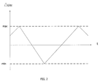
- Fig. 2 shows the regulation of the source voltage.
- the control logic 4 produces a predetermined interval [min, max].
- the predetermined interval is symmetrical and centered on zero, for example [-1V, + 1V]. Note that this interval can also be open.
- the control logic 4 receives on the interface 10 a source setpoint voltage U * DC .
- This source setpoint voltage U * DC is preferably a filtered value of a measurement of the source voltage. It can also be an estimation of the source voltage, for example using a Kalman or Luenberger type state reconstructor. This filtered value or this estimate makes it possible to limit the undulations of the voltage around an average of the source voltage.
- the control logic 4 acquires the measurement of the source voltage U DC .
- the control logic 4 can acquire this measurement of the source voltage U DC , which is also the DC bus voltage, by measuring the voltage near the inverter 1. It can also acquire the measurement of the source voltage U DC by estimates or indirect measures.
- the control logic 4 calculates the instantaneous source voltage error ⁇ U DC .
- ⁇ U DC is the difference between the source voltage U DC and the setpoint voltage U * DC .
- the instantaneous source voltage error ⁇ U DC is maintained by the control logic 4 in the predetermined interval [min, max] otherwise the control of the load could be lost.
- the control logic elects a control vector for which the source voltage U DC is as close as possible to the desired voltage value U * DC . It applies this elected control vector to the inverter.
- the regulation of the source voltage U DC can be carried out, in one example, by two methods. In a first method, the source voltage U DC is regulated according to a predictive strategy. And in a second method, the source voltage U DC is regulated according to a hysteretic strategy.
- the control logic 4 implements a predictive strategy.
- the predictive strategy is based on a predetermined modeling of the impedance of the DC bus. This predetermined modeling of the impedance of the DC bus represents the predictive model of the DC bus.
- the control logic 4 confronts the modeling of the continuous bus with the possible control vectors. From this confrontation, it elects the control vector making it possible to reduce the error in the predetermined interval.
- the modeling of the continuous bus thus makes it possible to simulate the response of the continuous bus to a given control vector. This simulation makes it possible to test the different vectors of possible commands to elect the one that corresponds most to a predetermined criterion.
- the regulation of the source voltage by the predictive strategy is intended to predict the evolution of the voltage U DC when it is necessary to switch the switches of the bridge arms of the inverter so as to choose the best possible switching.
- This source voltage strategy makes it possible to control the ripple of the source voltage when the decoupling capacitance is of low value. Indeed, it will be noted that with low-value capacitors, from the slightest parasitic inductance, there appears a resonant circuit upstream of the inverter, leading to ripples of the voltage of the power source. These ripples can cause the irreversible destruction of the switches of the inverter by exceeding the admissible reverse voltage at their terminals. This disrupts the supply of potential electrical consumers, including the headlights in the case of a motor vehicle, connected in parallel to the voltage source.
- the control logic 4 implements a hysteretic strategy.
- the control logic 4 elects a control vector allowing, when it is applied to the inverter 1, to create a current step to the input of the inverter 1 correcting the direction of variation of the source voltage U DC . If the instantaneous source voltage error ⁇ U DC is greater than the maximum of the predetermined interval then the control logic 4 imposes a positive source current step causing a sufficient break in the slope for the source voltage to change. sense of evolution. Similarly, if the instantaneous source voltage error ⁇ U DC is smaller than the min of the predetermined interval then the control logic 4 imposes a negative source current step.
- the hysteretic strategy makes it possible to dispense with the knowledge of the predictive model of the continuous bus, this model being difficult to obtain because it is necessary to measure parasitic elements, i.e. of very low values.
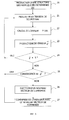
- Fig. 3 shows an embodiment of the invention in which the predictive strategy is coupled to a predictive current control of the load 3 or to a voltage vector control of the load 3 so as to have both a control upstream and downstream of the inverter 1.
- the control logic 4 produces in step 20 a predetermined geometric structure.
- the control logic 4 produces in step 20 a first part of the geometrical structure (necessary for the downstream control) and a second part of this geometrical structure which is the predetermined interval [min, max] (necessary for upstream control).
- the production of the first part of the geometrical structure depends on the control of the load 3.
- the inverter 1 drives the load 3 in current.
- the control logic 4 acquires the measurements of the currents of each phase of the load 3.
- the control logic 4 can acquire these measurements either by taking measurements in the phases of the load 3 or by making estimates or indirect measurements.
- the set of phase currents can be represented by a current vector in I ⁇ the stator mark.
- the control logic 4 receives at the interface 10 a reference current vector I * ⁇ .
- the control logic 4 calculates the current vector error.
- the current vector error ( ⁇ lx, ⁇ ly) is the difference between the current vector I ⁇ and the current vector I * ⁇ .
- the current vector error In order for the current control of the load to be optimal, the current vector error must be as low as possible.
- the current vector error is then circumscribed in a field of the plane, by the control logic 4.
- This area of the plane is the first part of the predetermined geometrical structure produced by the control logic 4 to step 20. In a preferred embodiment, this area of the plane is a disk. This makes it easy to detect the outputs of the plan area.
- control logic 4 When the vector error of current leaves the disk, then the control logic 4 confronts possible control vectors with a modeling of the load 3. From this confrontation, the control logic 4 elects the control vector reducing the vector error of current in the disk.
- the inverter 1 drives the load 3 in voltage.
- the control logic 4 acquires the measurements of the voltages of each phase of the load 3.
- the control logic 4 can acquire these measurements either by taking measurements in the phases of the load 3 or by making estimates or indirect measurements.
- the set of phase voltages can be represented by a voltage vector in the stator reference.
- the control logic 4 receives at the interface 10 a target voltage vector V ⁇ * .
- the control logic 4 calculates the voltage vector error.
- the voltage vector error is the difference between the target voltage vector V ⁇ * and the voltage vector V ⁇ .
- the average value of the standard of the voltage vector error must be as small as possible.
- the control logic 4 then performs a transformation of the voltage vector error which can, in turn, be canceled.
- control logic can cancel the voltage vector error as a mean value.
- the cancellation of the mean value of the voltage vector error is obtained by a time integral of said voltage vector error.
- the transformation of the voltage vector error is a Integral in time of the voltage vector error.
- the control logic 4 In order for the voltage vector control of the load 3 to be of good quality, i.e. optimal, it is necessary that the integral over time of the vector voltage error is as small as possible.
- the control logic 4 then circumscribes the integral vector of the voltage vector error in a domain of the plane, i.e., maintains it within this range of the plane.
- This area of the plane is the first part of the predetermined geometrical structure produced by the control logic 4 in step 20. In a preferred embodiment, this area of the plane is a disk.
- control logic 4 When the integral of the vector error of voltage leaves the disk then the control logic 4 confronts the possible control vectors with the corresponding evolution of the corresponding error vector transform.
- the control logic 4 elects a control vector reducing the integral of the voltage vector error in the disk.
- the vector is elected according to an exemplary embodiment illustrated in FIG. 5, which will be detailed later in the description.
- the predetermined geometric structure comprises at least two dimensions regardless of the number of phases of the charge 3. In the example taken, there are three phases, and the geometric structure has two dimensions because it is a disk.
- the control logic 4 After determining the predetermined geometrical structure by the control logic 4 in step 20, the control logic 4 measures or estimates the source voltage U DC in step 21. In step 22, the control logic 4 calculates the instantaneous source voltage error ⁇ U DC as a function of the setpoint voltage U * DC . This instantaneous source voltage error ⁇ U DC is the difference between the source voltage U DC and the setpoint voltage U * DC .
- the control logic 4 must maintain, on the one hand, the vector error while current in a disk, in the case of current control, or the integral of the voltage vector error in a disk, in the case of voltage control, and secondly the instantaneous source voltage error ⁇ U DC in the predetermined range by a predictive strategy.
- the control logic 4 defines, in step 23, an error vector ⁇ ⁇ representing the concatenation of the current vector error ( ⁇ Ix, ⁇ ly) (downstream control) or the integral of the voltage vector error and the source voltage error ⁇ U DC (upstream control).
- the purpose of the strategy is therefore to define the state of the switches of the polyphase inverter so that the vector error ⁇ ⁇ (( ⁇ lx, ⁇ ly, ⁇ U DC ) remains permanently in the predetermined geometrical structure.
- This predetermined geometrical structure is a volume. This volume represents the first part of the predetermined geometrical structure and the predetermined interval. part of the predetermined geometric structure is a disk then the space domain of the error vector ⁇ ⁇ is a cylinder.
- the first part of the predetermined geometrical structure comprises at least two dimensions regardless of the number of phases of the charge 3. In the example taken, there are three phases, and the first part of the geometric structure has two dimensions. because it's a record. Furthermore, the coupling of the dimensions of the first part of the geometrical structure with the size of the instantaneous source voltage error extends this structure to an additional dimension.
- the predetermined geometrical structure produced in step 20 is therefore a cylinder, a 3-dimensional structure.
- control logic 4 is able at any time to estimate the trajectory of the vector error ⁇ ⁇ in the space.
- the control logic 4 can therefore optimally determine the control vector of the inverter to maintain the error in the cylinder.
- step 24 the control logic 4 constantly polls the error vector ⁇ ⁇ to see if he's in the cylinder. If it is outside the cylinder, then the control logic 4 determines, in step 25, whether the error vector ⁇ ⁇ converges towards the cylinder. In case, the error vector ⁇ ⁇ converges to the cylinder then the control logic 4 maintains the same control vector of the inverter 1. When the error vector ⁇ ⁇ does not converge towards the cylinder, then the control logic 4 elects, in step 26, a new control vector reducing the error vector ⁇ ⁇ in the cylinder. The election criteria of the new control vector, in step 26, are described in FIG. 5. In step 27 the control logic 4 controls the inverter 1 with this new control vector.
- Fig. Figure 5 shows the different steps of an election of a control vector for the predictive strategies.
- the control logic 4 determines in step 61 the accessible control vectors and the non-accessible control vectors of the bridge arms of the inverter 1.
- the accessible control vectors are the command vectors requiring only a single switching on a single bridge arm with respect to the current status of the inverter 1.
- the non-accessible control vectors are the remaining control vectors.
- step 62 the control logic 4 determines in the accessible control vectors those reducing the error in its geometric structure. Then, it determines among these control vectors that maximizing the appearance time of the next error.
- the control logic 4 controls the inverter this accessible control vector.
- control logic 4 checks in step 63 if one of the non-accessible control vectors reduces the error in its geometrical structure. Then, it determines among these control vectors that maximizing the time of occurrence of the next error to reduce switching losses in the inverter.
- the control logic 4 controls the inverter with this non-accessible control vector.
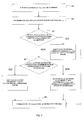
- Fig. 4 shows another embodiment in which the hysteretic strategy is coupled to a current control of the load 3 so as to have both a control upstream and downstream of the inverter 1.
- the inverter 1 drives the load 3 electric polyphase current.
- the control logic 4 produces in step 30 a hysteresis.
- the hysteresis makes it possible to compare a scalar current error of each phase of the load 3 with two predefined and different current error thresholds. To produce a hysteresis is thus to produce an interval [ ⁇ H1, ⁇ H2].
- the hysteresis defines the current error threshold ⁇ H1 for which it produces at its output a control of the phase (here at + U DC ). It also defines the current error threshold ⁇ H2 for which it stops the production of the control of the phase (here at 0).
- step 31 the control logic 4 produces the predetermined interval [min, max]. It measures or estimates the source voltage U DC , in step 32.
- step 33 the control logic 4 calculates the instantaneous source voltage error ⁇ U DC as a function of the reference voltage U * DC .
- step 34 the control logic 4 continuously polls the instantaneous source voltage error ⁇ U DC to check whether it is in the predetermined interval. If the instantaneous source voltage error ⁇ U DC is in the predetermined interval, the control logic 4 applies step 50. If the instantaneous source voltage error ⁇ U DC is outside the predetermined interval, the control logic 4 applies step 35.
- Step 50 corresponds to the control of the load 3, downstream of the inverter 1.
- Step 35 corresponds to the control of the source voltage, upstream of the inverter.
- the control of the upstream part of the inverter has priority over the control of the downstream part of the inverter.
- the result of the election to maintain the instantaneous source voltage error ⁇ U DC in the predetermined interval overrides the output of the hysteresis. Indeed, if we lose control upstream, we lose control downstream, ie if we do not have the necessary voltage upstream, we can not apply the necessary currents downstream.
- step 35 the control logic 4 checks whether the source voltage instantaneous error ⁇ U DC is greater than or equal to the maximum of the predetermined interval. If this is the case, then the control logic 4 determines in step 36 the convergence of the instantaneous source voltage error ⁇ U DC to the predetermined interval. If the instantaneous source voltage error ⁇ U DC converges to the predetermined interval then the control logic 4 maintains the same control vector.
- control logic 4 elects, in step 37, a new control vector, as previously described, returning the instantaneous error of source voltage ⁇ U DC in the predetermined range.
- step 35 the control logic 4 checks, in step 38, whether the instantaneous source voltage error ⁇ U DC is lower or equal to min of the predetermined interval. If this is the case, then the control logic 4 determines, in step 39, the convergence of the instantaneous source voltage error ⁇ U DC to the predetermined interval. If the instantaneous source voltage error ⁇ U DC converges to the predetermined interval then the control logic 4 maintains the same control vector.
- control logic 4 elects, in step 37, a new control vector reducing the instantaneous source voltage error ⁇ U DC in the predetermined interval.
- step 50 the control logic 4 measures or estimates the currents of each phase of the load 3.
- the control logic 4 receives at interface 10 a setpoint current.
- the control logic 4 calculates the current error of each phase of the load 3, in step 51.
- the current error is equal to the difference between the phase current and the reference current.
- step 52 the control logic 4 confronts each error of current of each phase of the charge 3 to the hysteresis.
- the hysteresis produces at its output a control of the phase for each of the phases of the load 3. These phase controls determine the state of each bridge arm of the corresponding inverter.
- the current control of the load defines the state of a bridge arm of the polyphase inverter as a function of the phase current error therein. Depending on this error in the corresponding arm, one chooses to change the control vector according to the principle of hysteresis.
- the output state number of the hysteresis is equal to the number of output levels of the polyphase inverter being controlled.
- the control logic 4 determines, in step 53, the convergence of the current error with respect to the hysteresis.
- the control logic 4 maintains the command controlling this bridge arm. This is valid for all bridge arms of the inverter.
- control logic 4 produces a new control of the phase, in step 54, for this bridge arm. This is valid for all the bridge arms of the inverter, so we have a hysteresis per arm and therefore per phase of the load 3.
- step 40 the control logic 4 controls the inverter 1 with this new control vector
- Load 3 can be controlled by a variant of the hysteretic strategy coupled to the current control of the load.
- This variant is used when the load is isolated neutral, ie the neutral point of the load phases is not connected to a potential.
- one of the hysteresis for the control of the corresponding phases is redundant. Indeed in this case, the sum of the phase currents is always equal to 0.
- one of the bridge arms is no longer really controllable current.
- control logic 4 modifies the operating mode of the hysteresis.
- the control logic 4 performs the current control, by comparing the errors of each phase of the load at hysteresis, on N-1 bridge arm. It performs a voltage check on the remaining bridge arm. N being the number of phases of the charge 3. There is as much phase as there are bridge arms.
- control logic 4 controls in voltage the bridge arm having the largest phase current by blocking the latter.
- Blocking means of a bridge arm maintains said bridge arm in a given state. In other words, the states of the switches of said bridge arm do not change.
- the control logic 4 makes it possible to alternately switch the set of bridge arms of the inverter.
- the gain is to no longer switch the bridge arms when the current in the latter is maximum and thus reduce the losses by switching in the switches.
- the control logic 4 blocks the second bridge arm having the largest phase current. If the latter is not lockable, then the control logic 4 blocks the third bridge arm having the largest phase current, and so on.
- an advantage of coupling with isolated neutral load is to optimally reduce switching losses.
Landscapes
- Engineering & Computer Science (AREA)
- Power Engineering (AREA)
- Inverter Devices (AREA)
Applications Claiming Priority (1)
| Application Number | Priority Date | Filing Date | Title |
|---|---|---|---|
| FR0508189A FR2889370B1 (fr) | 2005-07-29 | 2005-07-29 | Procede de commande d'un onduleur de tension polyphase |
Publications (3)
| Publication Number | Publication Date |
|---|---|
| EP1786090A2 true EP1786090A2 (de) | 2007-05-16 |
| EP1786090A3 EP1786090A3 (de) | 2013-03-13 |
| EP1786090B1 EP1786090B1 (de) | 2014-07-02 |
Family
ID=36182369
Family Applications (1)
| Application Number | Title | Priority Date | Filing Date |
|---|---|---|---|
| EP06115054.6A Not-in-force EP1786090B1 (de) | 2005-07-29 | 2006-06-07 | Steuerverfahren für Mehrphasenwechselrichter |
Country Status (4)
| Country | Link |
|---|---|
| US (1) | US7400102B2 (de) |
| EP (1) | EP1786090B1 (de) |
| JP (1) | JP2007043896A (de) |
| FR (1) | FR2889370B1 (de) |
Families Citing this family (7)
| Publication number | Priority date | Publication date | Assignee | Title |
|---|---|---|---|---|
| US7808195B2 (en) * | 2006-05-15 | 2010-10-05 | Mitsubishi Electric Corporation | Control apparatus for electric train |
| WO2009041157A1 (ja) * | 2007-09-27 | 2009-04-02 | Kabushiki Kaisha Yaskawa Denki | インバータ制御装置及びその制御方法 |
| JP5742110B2 (ja) * | 2010-04-14 | 2015-07-01 | 日産自動車株式会社 | 電力変換装置 |
| GB201114868D0 (en) * | 2011-08-30 | 2011-10-12 | Rolls Royce Plc | Method of controlling an inverter and a controller for controlling an inverter |
| US9484840B2 (en) * | 2013-08-28 | 2016-11-01 | University Of Central Florida Research Foundation, Inc. | Hybrid zero-voltage switching (ZVS) control for power inverters |
| JP6540538B2 (ja) * | 2016-02-24 | 2019-07-10 | 株式会社デンソー | 交流電動機の制御装置 |
| EP3576284A1 (de) | 2018-05-30 | 2019-12-04 | Siemens Aktiengesellschaft | Elektrisches koppeln eines ersten elektrischen netzes mit einem zweiten elektrischen netz |
Family Cites Families (9)
| Publication number | Priority date | Publication date | Assignee | Title |
|---|---|---|---|---|
| JPS5658781A (en) * | 1979-10-19 | 1981-05-21 | Hitachi Ltd | Controlling method of inverter equipment |
| JPS61154483A (ja) * | 1984-12-27 | 1986-07-14 | Mitsubishi Electric Corp | 多重インバ−タ装置 |
| JPS61258677A (ja) * | 1985-05-07 | 1986-11-17 | Mitsubishi Electric Corp | 電圧形インバ−タ制御方法 |
| US4648022A (en) * | 1986-02-14 | 1987-03-03 | Westinghouse Electric Corp. | Matrix converter control system |
| US5010291A (en) * | 1990-05-29 | 1991-04-23 | Westinghouse Electric Corp. | Single quadrant chopper timing control circuit for discontinuous current |
| US5111374A (en) * | 1990-06-22 | 1992-05-05 | The University Of Tennessee Research Corp. | High frequency quasi-resonant DC voltage notching scheme of a PWM voltage fed inverter for AC motor drives |
| US5818192A (en) * | 1995-08-04 | 1998-10-06 | The Boeing Company | Starting of synchronous machine without rotor position of speed measurement |
| US6118680A (en) * | 1999-05-28 | 2000-09-12 | Peco Ii | Methods and apparatus for load sharing between parallel inverters in an AC power supply |
| US6876176B2 (en) * | 2000-12-02 | 2005-04-05 | Ford Global Technologies, Llc | Toroidally wound induction motor-generator with selectable number of poles and vector control |
-
2005
- 2005-07-29 FR FR0508189A patent/FR2889370B1/fr not_active Expired - Fee Related
-
2006
- 2006-06-07 EP EP06115054.6A patent/EP1786090B1/de not_active Not-in-force
- 2006-06-26 US US11/474,327 patent/US7400102B2/en active Active
- 2006-07-26 JP JP2006202693A patent/JP2007043896A/ja active Pending
Also Published As
| Publication number | Publication date |
|---|---|
| JP2007043896A (ja) | 2007-02-15 |
| US20070025130A1 (en) | 2007-02-01 |
| US7400102B2 (en) | 2008-07-15 |
| FR2889370A1 (fr) | 2007-02-02 |
| FR2889370B1 (fr) | 2007-09-07 |
| EP1786090B1 (de) | 2014-07-02 |
| EP1786090A3 (de) | 2013-03-13 |
Similar Documents
| Publication | Publication Date | Title |
|---|---|---|
| EP1632019A1 (de) | Steuergerät mit pulsbreitenmodulation für eine vielseitigeinsetzbare elektrische maschine und eine vielseitigeinsetzbare elektrische maschine ausgesttatet mit einem solchen steuergerät | |
| EP3175528B1 (de) | Verfahren und vorrichtung zum laden einer batterie eines kraftfahrzeugs je nach impedanz eines energieversorgungsnetzes und kraftfahrzeug mit solch einer ladevorrichtung | |
| FR2894735A1 (fr) | Generateur-moteur synchrone a enroulement de champ | |
| EP1786090B1 (de) | Steuerverfahren für Mehrphasenwechselrichter | |
| EP3451525B1 (de) | Verfahren zur identifizierung der magnetischen sättigungsparameter eines asynchronen elektromotors | |
| EP1964257B1 (de) | Mehrphasen-spannungsumsetzer-steuerverfahren | |
| FR2968769A1 (fr) | Procede de determination de l'etat de sante d'une batterie pour l'alimentation d'un vehicule electrique | |
| EP2717409A1 (de) | Regulierung eines elektronischen Spannungsanpassungsmoduls | |
| FR3078050A1 (fr) | Procede de compensation d’un couple frein lors d’une defaillance de type court-circuit dans l’onduleur d’alimentation d’un moteur d’assistance | |
| FR3014263A1 (fr) | Procede de detection d'un defaut de fonctionnement d'un element de commutation actif d'un redresseur en pont de reseau de bord de vehicule automobile | |
| EP2870018B1 (de) | Verfahren zur steuerung eines antriebsstranges und entsprechendes system | |
| FR2733096A1 (fr) | Procede de regulation de vitesse d'un moteur electrique | |
| FR3049788A1 (fr) | Procede de commande d'un moteur electrique asynchrone | |
| FR2920884A1 (fr) | Procede d'estimation de l'etat de sante d'une batterie embarquee dans un vehicule automobile. | |
| EP1964256B1 (de) | Verfahren zur steuerung eines mehrphasen-spannungswechselrichters | |
| EP4551424A1 (de) | Kalibrierung, überprüfung und effizienzverbesserung eines antriebs einer elektrischen maschine | |
| EP4229748A1 (de) | Verfahren und system zur steuerung einer elektrischen maschine zur bestimmung optimaler stromsollwerte | |
| FR2853081A1 (fr) | Systeme et procede de determination de l'etat de charge instantane d'une batterie, et utilisation de ce procede dans un gestionnaire de charge | |
| EP2940849B1 (de) | Elektrische stromversorgung und steuerverfahren einer solchen elektrischen stromversorgung | |
| FR3157034A1 (fr) | Procédé de calcul d’un angle du vecteur flux d’inducteur, et dispositif correspondant | |
| FR2909816A1 (fr) | Appareil de commande de generateur de courant alternatif (ca) pour vehicule | |
| FR2982680A1 (fr) | Procede et systeme de commande pour corriger les tensions a appliquer a une charge electrique | |
| WO2006024802A1 (fr) | Procede d'évaluation de l'etat d'une batterie electrochimique et dispositif de mise en œuvre | |
| EP4047813B1 (de) | Regulierungsmodul für elektrisch umlaufende maschine | |
| FR2854007A1 (fr) | Procede de regulation d'un generateur electrique |
Legal Events
| Date | Code | Title | Description |
|---|---|---|---|
| PUAI | Public reference made under article 153(3) epc to a published international application that has entered the european phase |
Free format text: ORIGINAL CODE: 0009012 |
|
| 17P | Request for examination filed |
Effective date: 20060607 |
|
| AK | Designated contracting states |
Kind code of ref document: A2 Designated state(s): AT BE BG CH CY CZ DE DK EE ES FI FR GB GR HU IE IS IT LI LT LU LV MC NL PL PT RO SE SI SK TR |
|
| AX | Request for extension of the european patent |
Extension state: AL BA HR MK YU |
|
| PUAL | Search report despatched |
Free format text: ORIGINAL CODE: 0009013 |
|
| AK | Designated contracting states |
Kind code of ref document: A3 Designated state(s): AT BE BG CH CY CZ DE DK EE ES FI FR GB GR HU IE IS IT LI LT LU LV MC NL PL PT RO SE SI SK TR |
|
| AX | Request for extension of the european patent |
Extension state: AL BA HR MK RS |
|
| RIC1 | Information provided on ipc code assigned before grant |
Ipc: H02M 7/5387 20070101AFI20130207BHEP |
|
| AKX | Designation fees paid |
Designated state(s): AT BE BG CH CY CZ DE DK EE ES FI FR GB GR HU IE IS IT LI LT LU LV MC NL PL PT RO SE SI SK TR |
|
| GRAJ | Information related to disapproval of communication of intention to grant by the applicant or resumption of examination proceedings by the epo deleted |
Free format text: ORIGINAL CODE: EPIDOSDIGR1 |
|
| GRAP | Despatch of communication of intention to grant a patent |
Free format text: ORIGINAL CODE: EPIDOSNIGR1 |
|
| INTG | Intention to grant announced |
Effective date: 20140121 |
|
| GRAS | Grant fee paid |
Free format text: ORIGINAL CODE: EPIDOSNIGR3 |
|
| GRAA | (expected) grant |
Free format text: ORIGINAL CODE: 0009210 |
|
| AK | Designated contracting states |
Kind code of ref document: B1 Designated state(s): AT BE BG CH CY CZ DE DK EE ES FI FR GB GR HU IE IS IT LI LT LU LV MC NL PL PT RO SE SI SK TR |
|
| REG | Reference to a national code |
Ref country code: GB Ref legal event code: FG4D Free format text: NOT ENGLISH |
|
| REG | Reference to a national code |
Ref country code: CH Ref legal event code: EP |
|
| REG | Reference to a national code |
Ref country code: IE Ref legal event code: FG4D Free format text: LANGUAGE OF EP DOCUMENT: FRENCH |
|
| REG | Reference to a national code |
Ref country code: DE Ref legal event code: R096 Ref document number: 602006042112 Country of ref document: DE Effective date: 20140814 |
|
| REG | Reference to a national code |
Ref country code: NL Ref legal event code: VDEP Effective date: 20140702 |
|
| REG | Reference to a national code |
Ref country code: AT Ref legal event code: REF Ref document number: 700046 Country of ref document: AT Kind code of ref document: T Effective date: 20141215 |
|
| REG | Reference to a national code |
Ref country code: LT Ref legal event code: MG4D |
|
| PG25 | Lapsed in a contracting state [announced via postgrant information from national office to epo] |
Ref country code: SE Free format text: LAPSE BECAUSE OF FAILURE TO SUBMIT A TRANSLATION OF THE DESCRIPTION OR TO PAY THE FEE WITHIN THE PRESCRIBED TIME-LIMIT Effective date: 20140702 Ref country code: GR Free format text: LAPSE BECAUSE OF FAILURE TO SUBMIT A TRANSLATION OF THE DESCRIPTION OR TO PAY THE FEE WITHIN THE PRESCRIBED TIME-LIMIT Effective date: 20141003 Ref country code: FI Free format text: LAPSE BECAUSE OF FAILURE TO SUBMIT A TRANSLATION OF THE DESCRIPTION OR TO PAY THE FEE WITHIN THE PRESCRIBED TIME-LIMIT Effective date: 20140702 Ref country code: PT Free format text: LAPSE BECAUSE OF FAILURE TO SUBMIT A TRANSLATION OF THE DESCRIPTION OR TO PAY THE FEE WITHIN THE PRESCRIBED TIME-LIMIT Effective date: 20141103 Ref country code: LT Free format text: LAPSE BECAUSE OF FAILURE TO SUBMIT A TRANSLATION OF THE DESCRIPTION OR TO PAY THE FEE WITHIN THE PRESCRIBED TIME-LIMIT Effective date: 20140702 Ref country code: CZ Free format text: LAPSE BECAUSE OF FAILURE TO SUBMIT A TRANSLATION OF THE DESCRIPTION OR TO PAY THE FEE WITHIN THE PRESCRIBED TIME-LIMIT Effective date: 20140702 Ref country code: BG Free format text: LAPSE BECAUSE OF FAILURE TO SUBMIT A TRANSLATION OF THE DESCRIPTION OR TO PAY THE FEE WITHIN THE PRESCRIBED TIME-LIMIT Effective date: 20141002 Ref country code: ES Free format text: LAPSE BECAUSE OF FAILURE TO SUBMIT A TRANSLATION OF THE DESCRIPTION OR TO PAY THE FEE WITHIN THE PRESCRIBED TIME-LIMIT Effective date: 20140702 |
|
| PG25 | Lapsed in a contracting state [announced via postgrant information from national office to epo] |
Ref country code: CY Free format text: LAPSE BECAUSE OF FAILURE TO SUBMIT A TRANSLATION OF THE DESCRIPTION OR TO PAY THE FEE WITHIN THE PRESCRIBED TIME-LIMIT Effective date: 20140702 Ref country code: IS Free format text: LAPSE BECAUSE OF FAILURE TO SUBMIT A TRANSLATION OF THE DESCRIPTION OR TO PAY THE FEE WITHIN THE PRESCRIBED TIME-LIMIT Effective date: 20141102 Ref country code: PL Free format text: LAPSE BECAUSE OF FAILURE TO SUBMIT A TRANSLATION OF THE DESCRIPTION OR TO PAY THE FEE WITHIN THE PRESCRIBED TIME-LIMIT Effective date: 20140702 Ref country code: LV Free format text: LAPSE BECAUSE OF FAILURE TO SUBMIT A TRANSLATION OF THE DESCRIPTION OR TO PAY THE FEE WITHIN THE PRESCRIBED TIME-LIMIT Effective date: 20140702 Ref country code: NL Free format text: LAPSE BECAUSE OF FAILURE TO SUBMIT A TRANSLATION OF THE DESCRIPTION OR TO PAY THE FEE WITHIN THE PRESCRIBED TIME-LIMIT Effective date: 20140702 |
|
| REG | Reference to a national code |
Ref country code: AT Ref legal event code: MK05 Ref document number: 700046 Country of ref document: AT Kind code of ref document: T Effective date: 20140702 |
|
| REG | Reference to a national code |
Ref country code: DE Ref legal event code: R097 Ref document number: 602006042112 Country of ref document: DE |
|
| PG25 | Lapsed in a contracting state [announced via postgrant information from national office to epo] |
Ref country code: EE Free format text: LAPSE BECAUSE OF FAILURE TO SUBMIT A TRANSLATION OF THE DESCRIPTION OR TO PAY THE FEE WITHIN THE PRESCRIBED TIME-LIMIT Effective date: 20140702 Ref country code: IT Free format text: LAPSE BECAUSE OF FAILURE TO SUBMIT A TRANSLATION OF THE DESCRIPTION OR TO PAY THE FEE WITHIN THE PRESCRIBED TIME-LIMIT Effective date: 20140702 Ref country code: DK Free format text: LAPSE BECAUSE OF FAILURE TO SUBMIT A TRANSLATION OF THE DESCRIPTION OR TO PAY THE FEE WITHIN THE PRESCRIBED TIME-LIMIT Effective date: 20140702 Ref country code: SK Free format text: LAPSE BECAUSE OF FAILURE TO SUBMIT A TRANSLATION OF THE DESCRIPTION OR TO PAY THE FEE WITHIN THE PRESCRIBED TIME-LIMIT Effective date: 20140702 Ref country code: RO Free format text: LAPSE BECAUSE OF FAILURE TO SUBMIT A TRANSLATION OF THE DESCRIPTION OR TO PAY THE FEE WITHIN THE PRESCRIBED TIME-LIMIT Effective date: 20140702 |
|
| PLBE | No opposition filed within time limit |
Free format text: ORIGINAL CODE: 0009261 |
|
| STAA | Information on the status of an ep patent application or granted ep patent |
Free format text: STATUS: NO OPPOSITION FILED WITHIN TIME LIMIT |
|
| PG25 | Lapsed in a contracting state [announced via postgrant information from national office to epo] |
Ref country code: AT Free format text: LAPSE BECAUSE OF FAILURE TO SUBMIT A TRANSLATION OF THE DESCRIPTION OR TO PAY THE FEE WITHIN THE PRESCRIBED TIME-LIMIT Effective date: 20140702 |
|
| 26N | No opposition filed |
Effective date: 20150407 |
|
| PG25 | Lapsed in a contracting state [announced via postgrant information from national office to epo] |
Ref country code: SI Free format text: LAPSE BECAUSE OF FAILURE TO SUBMIT A TRANSLATION OF THE DESCRIPTION OR TO PAY THE FEE WITHIN THE PRESCRIBED TIME-LIMIT Effective date: 20140702 |
|
| PG25 | Lapsed in a contracting state [announced via postgrant information from national office to epo] |
Ref country code: MC Free format text: LAPSE BECAUSE OF FAILURE TO SUBMIT A TRANSLATION OF THE DESCRIPTION OR TO PAY THE FEE WITHIN THE PRESCRIBED TIME-LIMIT Effective date: 20140702 |
|
| REG | Reference to a national code |
Ref country code: CH Ref legal event code: PL |
|
| GBPC | Gb: european patent ceased through non-payment of renewal fee |
Effective date: 20150607 |
|
| PG25 | Lapsed in a contracting state [announced via postgrant information from national office to epo] |
Ref country code: LU Free format text: LAPSE BECAUSE OF FAILURE TO SUBMIT A TRANSLATION OF THE DESCRIPTION OR TO PAY THE FEE WITHIN THE PRESCRIBED TIME-LIMIT Effective date: 20150607 |
|
| REG | Reference to a national code |
Ref country code: IE Ref legal event code: MM4A |
|
| PG25 | Lapsed in a contracting state [announced via postgrant information from national office to epo] |
Ref country code: GB Free format text: LAPSE BECAUSE OF NON-PAYMENT OF DUE FEES Effective date: 20150607 Ref country code: CH Free format text: LAPSE BECAUSE OF NON-PAYMENT OF DUE FEES Effective date: 20150630 Ref country code: LI Free format text: LAPSE BECAUSE OF NON-PAYMENT OF DUE FEES Effective date: 20150630 Ref country code: IE Free format text: LAPSE BECAUSE OF NON-PAYMENT OF DUE FEES Effective date: 20150607 |
|
| REG | Reference to a national code |
Ref country code: FR Ref legal event code: PLFP Year of fee payment: 11 |
|
| PG25 | Lapsed in a contracting state [announced via postgrant information from national office to epo] |
Ref country code: HU Free format text: LAPSE BECAUSE OF FAILURE TO SUBMIT A TRANSLATION OF THE DESCRIPTION OR TO PAY THE FEE WITHIN THE PRESCRIBED TIME-LIMIT; INVALID AB INITIO Effective date: 20060607 |
|
| REG | Reference to a national code |
Ref country code: FR Ref legal event code: PLFP Year of fee payment: 12 |
|
| PG25 | Lapsed in a contracting state [announced via postgrant information from national office to epo] |
Ref country code: BE Free format text: LAPSE BECAUSE OF NON-PAYMENT OF DUE FEES Effective date: 20150630 |
|
| PG25 | Lapsed in a contracting state [announced via postgrant information from national office to epo] |
Ref country code: TR Free format text: LAPSE BECAUSE OF FAILURE TO SUBMIT A TRANSLATION OF THE DESCRIPTION OR TO PAY THE FEE WITHIN THE PRESCRIBED TIME-LIMIT Effective date: 20140702 |
|
| REG | Reference to a national code |
Ref country code: FR Ref legal event code: PLFP Year of fee payment: 13 |
|
| PGFP | Annual fee paid to national office [announced via postgrant information from national office to epo] |
Ref country code: DE Payment date: 20200612 Year of fee payment: 15 Ref country code: FR Payment date: 20200630 Year of fee payment: 15 |
|
| REG | Reference to a national code |
Ref country code: DE Ref legal event code: R119 Ref document number: 602006042112 Country of ref document: DE |
|
| PG25 | Lapsed in a contracting state [announced via postgrant information from national office to epo] |
Ref country code: DE Free format text: LAPSE BECAUSE OF NON-PAYMENT OF DUE FEES Effective date: 20220101 |
|
| PG25 | Lapsed in a contracting state [announced via postgrant information from national office to epo] |
Ref country code: FR Free format text: LAPSE BECAUSE OF NON-PAYMENT OF DUE FEES Effective date: 20210630 |