EP1786097A1 - Récépteur à compensation du décalage CC pour optimal IP2 - Google Patents
Récépteur à compensation du décalage CC pour optimal IP2 Download PDFInfo
- Publication number
- EP1786097A1 EP1786097A1 EP06123669A EP06123669A EP1786097A1 EP 1786097 A1 EP1786097 A1 EP 1786097A1 EP 06123669 A EP06123669 A EP 06123669A EP 06123669 A EP06123669 A EP 06123669A EP 1786097 A1 EP1786097 A1 EP 1786097A1
- Authority
- EP
- European Patent Office
- Prior art keywords
- offset
- mixer
- phase
- existing
- differential
- Prior art date
- Legal status (The legal status is an assumption and is not a legal conclusion. Google has not performed a legal analysis and makes no representation as to the accuracy of the status listed.)
- Granted
Links
- 238000000034 method Methods 0.000 claims description 32
- 230000008569 process Effects 0.000 claims description 13
- 238000010586 diagram Methods 0.000 description 6
- 230000004044 response Effects 0.000 description 6
- 230000008859 change Effects 0.000 description 3
- 230000003321 amplification Effects 0.000 description 2
- 238000006243 chemical reaction Methods 0.000 description 2
- 229920005994 diacetyl cellulose Polymers 0.000 description 2
- 238000003199 nucleic acid amplification method Methods 0.000 description 2
- 238000012546 transfer Methods 0.000 description 2
- 230000004075 alteration Effects 0.000 description 1
- 230000005540 biological transmission Effects 0.000 description 1
- 238000004891 communication Methods 0.000 description 1
- 230000001143 conditioned effect Effects 0.000 description 1
- 238000010276 construction Methods 0.000 description 1
- 230000007812 deficiency Effects 0.000 description 1
- 230000000694 effects Effects 0.000 description 1
- 230000002708 enhancing effect Effects 0.000 description 1
- 230000006870 function Effects 0.000 description 1
- 238000011065 in-situ storage Methods 0.000 description 1
- 230000000737 periodic effect Effects 0.000 description 1
- 238000012545 processing Methods 0.000 description 1
- 238000006467 substitution reaction Methods 0.000 description 1
- 230000002277 temperature effect Effects 0.000 description 1
- 238000012360 testing method Methods 0.000 description 1
- 238000011144 upstream manufacturing Methods 0.000 description 1
Images

Classifications
-
- H—ELECTRICITY
- H03—ELECTRONIC CIRCUITRY
- H03D—DEMODULATION OR TRANSFERENCE OF MODULATION FROM ONE CARRIER TO ANOTHER
- H03D3/00—Demodulation of angle-, frequency- or phase- modulated oscillations
- H03D3/007—Demodulation of angle-, frequency- or phase- modulated oscillations by converting the oscillations into two quadrature related signals
- H03D3/008—Compensating DC offsets
Definitions
- the invention is directed, in general, to a communication system and, more specifically, to an offset balancer, a method of balancing an offset and a wireless receiver that employs the balancer or the method.
- Receivers employ a mixer to translate a higher input radio frequency (RF) to a lower baseband or intermediate frequency. This process is known as down-conversion when utilizing a difference frequency between the RF input signal and a local oscillator employed by the mixer for conversion.
- the mixer output signal amplitude and phase are proportional only to the RF input signal amplitude and phase and independent of local oscillator characteristics.
- mixer nonlinearities produce undesirable mixing products.
- a second-order nonlinearity associated with the mixer produces an undesirable intermodulation product between two RF input frequencies.
- two RF input signals having different frequencies that are provided to the mixer within its frequency band should not produce a cross-modulation signal since the ideal transfer characteristic of the mixer would be perfectly linear.
- non-ideal mixers have a transfer characteristic that is nonlinear to some degree corresponding to second-order and greater nonlinear terms.
- the second-order nonlinearity will cause a spurious cross-modulation signal to be generated from two in-band RF input signal frequencies applied to the mixer. If this spurious cross-modulation signal is too large, the performance of the mixer and the associated quality of reception are degraded.
- the second-order nonlinearity of the mixer is related to mixer imbalance wherein several mixer attributes typically contribute to this imbalance.
- devices used in the mixer should have identical or perfectly matched characteristics related to switching parameters or properties associated with conducting and not conducting states.
- phase errors associated with multiphase mixers may also contribute to mixer imbalance, as well. That is, if two local oscillator phases employed in the mixer differ from their intended phases, mixer imbalance will typically result.
- each of these characteristics contributes in some degree to increasing the mixer imbalance and its corresponding second-order nonlinearity. Therefore, mismatch contributions from such a broad-based combination of characteristics essentially assures some degree of imbalance in a mixer.
- the invention provides an offset balancer for use with a differential mixer employing a wireless reception and an offset quantifier configured to indicate an existing DC offset of the mixer corresponding to an existing second-order intercept point applicable to the wireless reception.
- the offset balancer includes an offset adjuster coupled to the offset quantifier and configured to provide an offset adjustment to the existing DC offset based on increasing the existing second-order intercept point.
- the invention provides a method of balancing an offset for use with a differential mixer employing a wireless reception and indicating an existing DC offset of the mixer corresponding to an existing second-order intercept point applicable to the wireless reception.
- the method includes providing an offset adjustment to the existing DC offset based on increasing the existing second-order intercept point.
- the invention also provides, in yet another aspect, a wireless receiver that includes a low noise amplifier, which processes a wireless reception and a differential mixer coupled to the low noise amplifier.
- the wireless receiver also includes an offset balancer coupled to the differential mixer and having an offset quantifier that indicates an existing DC offset of the mixer corresponding to an existing second-order intercept point applicable to the wireless reception.
- the offset balancer also has an offset adjuster, coupled to the offset quantifier, which provides an offset adjustment to the existing DC offset based on increasing the existing second-order intercept point.
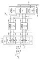
- the wireless receiver 100 includes a low noise amplifier 105 having an RF input 101, a transconductance amplifier 110, an in-phase/quadrature-phase (I/Q) mixer 115 having an in-phase differential mixer portion 120 coupled to an in-phase analog baseband filter 122 and a quadrature differential mixer portion 125 coupled to a quadrature analog baseband filter 127.
- the wireless receiver 100 also includes an offset balancer 130 having an offset quantifier 131 and an offset adjuster 132 that are coupled to a digital bus 135 and a memory 140.
- an alternative embodiment of the invention may employ single-ended mixer portions and baseband filters, as well.
- the low noise amplifier 105 is provided a receive signal at the RF input 101, which is amplified and provided to the transconductance amplifier 110.
- the transconductance amplifier 110 is employed to change a voltage output signal of the low noise amplifier 105 to a proportional current that is then applied to the I/Q mixer 115.
- the in-phase differential mixer portion 120 employs local oscillator phases of zero and 180 degrees to provide positive and negative differential in-phase outputs 121a, 121b to the in-phase analog baseband filter 122.
- the quadrature-phase differential mixer portion 125 employs local oscillator phases of 90 and 270 degrees to provide positive and negative differential quadrature-phase outputs 126a, 126b to the quadrature-phase baseband filter 127.
- the in-phase and quadrature-phase analog baseband filters 122, 127 respectively provide positive and negative, in-phase and quadrature-phase filtered differential outputs 123a, 123b, 128a, 128b to the offset quantifier 131.
- the offset quantifier 131 provides intermediate frequency amplification and digitization of the in-phase and quadrature-phase filtered differential outputs 123a, 123b, 128a, 128b wherein the digitized signals are provided to the digital bus 135 for further processing.
- the offset balancer 130 when the offset balancer 130 is employed to balance the I/Q mixer 115, the intermediate frequency amplification and digitization of the offset quantifier 131 is employed to indicate an existing DC offset of the I/Q mixer 115 that corresponds to an existing second-order intercept point IP2. Then, the offset adjuster 132, which is coupled to the offset quantifier 131, provides an offset adjustment to the existing DC offset based on increasing the existing second-order intercept point IP2.
- the offset adjustment is stored in the memory 140 for use by the offset adjuster 132 and is applied either to the in-phase and quadrature-phase filtered differential outputs 123a, 123b, 128a, 128b, as shown, or to the positive and negative differential in-phase and quadrature-phase outputs 121a, 121b, 126a, 126b as indicated in FIG. 1.
- the second-order intercept point IP2 is generally employed to characterize an amount of second-order nonlinearity that is associated with a mixer.
- the second-order intercept point IP2 is proportional to the linearity of the mixer and therefore, inversely proportional to its second-order nonlinearity.
- a greater value of the second-order intercept point IP2 indicates a lower second-order nonlinearity.
- An imbalance between the positive and negative outputs of a differential mixer degrades the second-order intercept point IP2 associated with the differential mixer. Therefore, imbalances in either the in-phase or quadrature-phase differential mixer portions 120, 125 degrade the performance of the I/Q mixer 115 in this regard.
- Embodiments of the invention are not attempting to force an existing DC offset to be zero, but rather, are establishing a predetermined or target value of DC offset that may be employed to increase the existing second-order intercept point IP2.
- This predetermined value of DC offset creates an "injected imbalance” or a "counter-imbalancing" offset between the positive and negative sides of the I/Q mixer 115, which counteracts and substantially nullifies the effect of a preexisting imbalance in the I/Q mixer 115. Therefore, this injected DC offset may be employed to provide a change in bias points of the I/Q mixer 115 such that it becomes more balanced overall.
- the target value of DC offset may be applied to only one of the in-phase or quadrature-phase differential mixer portions 120, 125 as appropriate to a particular application. Additionally, different predetermined values of DC offset for each of the in-phase or quadrature-phase differential mixer portions 120, 125 may be employed.
- Determination of the DC offset target values may be established through a calibration process.
- Calibration of the I/Q mixer 115 may be accommodated employing an off-line calibration process, such as a factory calibration, wherein the calibrating agents are external to the wireless receiver 100.
- calibration of the I/Q mixer 115 may be accomplished employing an on-line calibration process wherein the calibrating agents are provided in situ to the wireless receiver 100.
- two RF tones may be employed that produce an intermodulation product that falls within an appropriate frequency band.
- the offset adjustment to the existing DC offset is determined by reducing the intermodulation product to an acceptable level, based on existing constraints, to establish DC offset target values.
- These values may be directly employed by the offset adjuster 132, or other digitized values from the offset quantifier 131 may be employed that are directly proportional to the DC offset target values wherein either of these values may be stored for future use in the memory 140.
- the offset adjustment to the existing DC offset established during the initial off-line calibration process may need further adjustment to maintain an established level for the second-order intercept point IP2 due to temperature effects or component drift.
- the on-line calibration process may employ two or more tones (from an associated transmitter, for example) to make continual or periodic offset adjustment updates and thereby maintain or improve the initially established second-order intercept point IP2. Additionally, an analog loop back test employing two or more tones, initiated either digitally or from associated transmissions, may be used to verify proper operation of the wireless receiver 100.
- the offset balancer 200 includes an offset quantifier 210 and an offset adjuster 220.
- the offset quantifier 210 includes an in-phase intermediate frequency (IF) amplifier 211 coupled to an in-phase analog to digital converter (ADC) 212 and a quadrature-phase IF amplifier 213 coupled to a quadrature ADC 214 wherein both the in-phase and the quadrature-phase ADCs 212, 214, are further coupled to a digital bus 235 and a memory 240.
- IF intermediate frequency
- ADC analog to digital converter
- the offset adjuster 220 includes a digital signal processor (DSP) 221 coupled to the digital bus 235 and the memory 240, an in-phase digital to analog converter (DAC) group 222 and a quadrature-phase DAC group 223 coupled to the DSP 221.
- the offset adjuster 220 also includes in-phase positive and negative current sources 224a, 224b, and quadrature-phase positive and negative current sources 225a, 225b coupled to the in-phase and quadrature-phase DAC groups 222, 223, as shown.
- the offset quantifier 210 is coupled to in-phase and quadrature-phase outputs associated with a differential I/Q mixer employing positive and negative in-phase differential outputs 203a, 203b and positive and negative quadrature-phase differential outputs 208a, 208b.
- the offset quantifier 210 conditions and digitizes the differential in-phase and quadrature-phase mixer signals derived from a receive signal. This is accomplished with the in-phase IF amplifier 211 and ADC 212 and the quadrature-phase IF amplifier 213 and ADC 214.
- the offset adjuster 220 employs DC offset target values created by using appropriate offset adjustments to preexisting DC offsets, which were determined during a previous calibration phase and stored in the memory 240.
- the DSP 221 receives four stored digital DC offset target values from the memory 240 and respectively provides an appropriate one to the in-phase or quadrature-phase positive or negative DC offset DACs 222a, 222b, 223a, 223b.
- In-phase and quadrature-phase positive and negative current sources 224a, 224b, 225a, 225b convert the analog voltage outputs from each of the DC offset DACs 222a, 222b, 223a, 223b to corresponding currents for application to respective positive and negative in-phase and quadrature-phase differential outputs 203a, 203b, 208a, 208b, as shown.
- current sources are employed to provide the offsets, which would correspond to employing an upstream transconductance amplifier as was shown in FIG. 1.
- voltage sources may be employed to provide the offsets as appropriate to a particular application.
- Each of the positive and negative in-phase and quadrature-phase differential outputs 203a, 203b, 208a, 208b provide a separate DC offset target value thereby allowing independent adjustment of their offsets.
- In-phase and quadrature-phase applied differential offsets for each of the in-phase and quadrature-phase differential output pairs 203a, 203b and 208a, 208b may be determined as the algebraic difference between the respective separately provided in-phase and quadrature-phase DC offset target values. Therefore, the size and polarity of each of the in-phase and quadrature-phase applied differential offsets are adjusted by the offset balancer 200 to provide as much increase in the second-order intercept point IP2 of the mixer as allowed by other constraining circumstances.
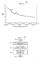
- FIG. 3 illustrated is a chart of an embodiment of a second-order intercept point IP2 response, generally designated 300, showing how mixer IP2 is impacted by DC offset adjustment.
- the chart 300 includes an IP2 response curve 305 associated with a differential mixer.
- the IP2 response curve 305 represents a second-order intercept point IP2 response that has been referred to the input of the differential mixer, which is designated as IIP2 in the chart 300.
- the IP2 response curve 305 shows how the second-order intercept point IP2 varies as a function of applied differential offset.
- An equivalent increase in the second-order intercept point IP2 of about 30 dBm may be observed as the applied differential offset varies from about a positive 4.5 millivolts to about a negative 3.5 millivolts.
- FIG. 4 illustrated is a flow diagram of an embodiment of a method of balancing an offset, generally designated 400, carried out in accordance with the principles of the invention.
- the method 400 is for use with a differential mixer employing a wireless reception and starts in a step 405.
- an existing DC offset of the mixer is indicated corresponding to an existing second-order intercept point IP2 applicable to the wireless reception.
- An offset adjustment is provided to the existing DC offset based on increasing the existing second-order intercept point IP2, in a step 415.
- the offset adjustment is determined in either an off-line or an on-line calibration process and then stored in a memory. Alternatively, a quantity directly proportional to the offset adjustment may be stored in the memory.
- the offset adjustment is employed for operational use with the differential mixer in a step 420.
- the offset adjustment provides a differential offset adjustment wherein at least one of an in-phase adjustment or a quadrature-phase adjustment is applied to the mixer, in the step 420.
- the offset adjustment may be provided to a direct output or a conditioned output of the mixer employing either a current-based or a voltage-based offset adjustment.
- the method 400 ends in a step 425.
- embodiments of the invention employing an offset balancer, a method of balancing an offset and a wireless receiver employing the balancer or the method have been presented.
- Advantages include increasing the second-order intercept point IP2 of a differential mixer by applying a targeted value of DC offset to the output of the mixer thereby enhancing the performance of the mixer. This corresponds to establishing a predetermined value of DC offset that creates an injected imbalance or a counter-imbalancing offset between the positive and negative sides of the differential mixer.
- the predetermined value of DC offset counteracts and substantially nullifies a preexisting imbalance of the mixer that allowed a lower value of the second-order intercept point IP2 to exist.
- This injected DC offset may be employed to provide a change in bias points of the mixer such that it becomes more balanced overall.
Landscapes
- Engineering & Computer Science (AREA)
- Power Engineering (AREA)
- Digital Transmission Methods That Use Modulated Carrier Waves (AREA)
- Amplifiers (AREA)
Applications Claiming Priority (1)
| Application Number | Priority Date | Filing Date | Title |
|---|---|---|---|
| US11/270,122 US7532874B2 (en) | 2005-11-09 | 2005-11-09 | Offset balancer, method of balancing an offset and a wireless receiver employing the balancer and the method |
Publications (2)
| Publication Number | Publication Date |
|---|---|
| EP1786097A1 true EP1786097A1 (fr) | 2007-05-16 |
| EP1786097B1 EP1786097B1 (fr) | 2010-01-13 |
Family
ID=37507851
Family Applications (1)
| Application Number | Title | Priority Date | Filing Date |
|---|---|---|---|
| EP06123669A Ceased EP1786097B1 (fr) | 2005-11-09 | 2006-11-08 | Récépteur à compensation du décalage CC pour optimal IP2 |
Country Status (3)
| Country | Link |
|---|---|
| US (1) | US7532874B2 (fr) |
| EP (1) | EP1786097B1 (fr) |
| DE (1) | DE602006011697D1 (fr) |
Cited By (3)
| Publication number | Priority date | Publication date | Assignee | Title |
|---|---|---|---|---|
| US8867671B2 (en) | 2010-06-15 | 2014-10-21 | Telefonaktiebolaget L M Ericsson (Publ) | Conversion circuit for converting complex analog signal into digital representation |
| US9450538B2 (en) | 2012-04-19 | 2016-09-20 | Telefonaktiebolaget Lm Ericsson (Publ) | Harmonic rejection mixer arrangement |
| US10317535B2 (en) | 2016-03-31 | 2019-06-11 | Samsung Electronics Co., Ltd | Method and apparatus for second order intercept point (IP2) calibration |
Families Citing this family (13)
| Publication number | Priority date | Publication date | Assignee | Title |
|---|---|---|---|---|
| US7826816B2 (en) * | 2006-07-11 | 2010-11-02 | Qualcomm Incorporated | Systems, methods, and apparatus for frequency conversion |
| US7894780B2 (en) * | 2006-12-06 | 2011-02-22 | Broadcom Corporation | Method and system for a linearized transmitter including a power amplifier |
| US7904048B2 (en) * | 2007-06-29 | 2011-03-08 | Texas Instruments Incorporated | Multi-tap direct sub-sampling mixing system for wireless receivers |
| US8010074B2 (en) * | 2008-02-08 | 2011-08-30 | Freescale Semiconductor, Inc. | Mixer circuits for second order intercept point calibration |
| KR101292666B1 (ko) | 2009-11-20 | 2013-08-02 | 한국전자통신연구원 | Dc 오프셋 제거 회로 |
| US8222944B2 (en) * | 2009-11-20 | 2012-07-17 | Electronics And Telecommunications Research Institute | DC offset cancellation circuit |
| US8787503B2 (en) * | 2012-09-18 | 2014-07-22 | Vixs Systems, Inc. | Frequency mixer with compensated DC offset correction to reduce linearity degradation |
| US8942656B2 (en) | 2013-03-15 | 2015-01-27 | Blackberry Limited | Reduction of second order distortion in real time |
| EP2779510B1 (fr) | 2013-03-15 | 2018-10-31 | BlackBerry Limited | Pondération statistique et ajustement de variables d'état dans une radio |
| US8983486B2 (en) | 2013-03-15 | 2015-03-17 | Blackberry Limited | Statistical weighting and adjustment of state variables in a radio |
| US9197279B2 (en) | 2013-03-15 | 2015-11-24 | Blackberry Limited | Estimation and reduction of second order distortion in real time |
| US8811538B1 (en) | 2013-03-15 | 2014-08-19 | Blackberry Limited | IQ error correction |
| US10191454B2 (en) * | 2016-06-13 | 2019-01-29 | William Marsh Rice University | Methods and related systems of ultra-short pulse detection |
Citations (5)
| Publication number | Priority date | Publication date | Assignee | Title |
|---|---|---|---|---|
| WO1998043357A2 (fr) * | 1997-03-21 | 1998-10-01 | Koninklijke Philips Electronics N.V. | Recepteur sans fil a compensation decalee utilisant un numeriseur parallele (adc) |
| US20040002311A1 (en) * | 2002-06-28 | 2004-01-01 | Shen Feng | Offset compensation in a direct-conversion receiver |
| US20040214547A1 (en) * | 2003-04-28 | 2004-10-28 | Samsung Electronics Co., Ltd. | Circuit and method for receiving and mixing radio frequencies in a direct conversion receiver |
| US20040230393A1 (en) * | 2003-05-14 | 2004-11-18 | Peter Andersson | Fast calibration of electronic components |
| WO2004109941A1 (fr) * | 2003-06-04 | 2004-12-16 | Koninklijke Philips Electronics, N.V. | Filtre adaptatif de distorsions d'intermodulation pour recepteurs zero-if |
Family Cites Families (8)
| Publication number | Priority date | Publication date | Assignee | Title |
|---|---|---|---|---|
| US6073002A (en) * | 1998-05-04 | 2000-06-06 | Motorola | Mixer circuit and communication device using the same |
| US6535725B2 (en) * | 2001-03-30 | 2003-03-18 | Skyworks Solutions, Inc. | Interference reduction for direct conversion receivers |
| WO2002084859A1 (fr) * | 2001-04-18 | 2002-10-24 | Nokia Corporation | Agencement de circuit equilibre et procede de linearisation de cet agencement |
| TWI260280B (en) * | 2002-05-31 | 2006-08-21 | Pentel Kk | Applicator |
| US20040087296A1 (en) * | 2002-10-25 | 2004-05-06 | Gct Semiconductor, Inc. | Radio receiver and method for AM suppression and DC-offset removal |
| US7062238B2 (en) * | 2002-12-20 | 2006-06-13 | General Motors Corporation | Radio frequency selection method and system for audio channel output |
| US20060141972A1 (en) * | 2003-02-20 | 2006-06-29 | Nec Corporation | Signal processing device and direct conversion reception device |
| JP4332095B2 (ja) * | 2004-10-01 | 2009-09-16 | パナソニック株式会社 | Dcオフセットキャリブレーションシステム |
-
2005
- 2005-11-09 US US11/270,122 patent/US7532874B2/en active Active
-
2006
- 2006-11-08 DE DE602006011697T patent/DE602006011697D1/de active Active
- 2006-11-08 EP EP06123669A patent/EP1786097B1/fr not_active Ceased
Patent Citations (5)
| Publication number | Priority date | Publication date | Assignee | Title |
|---|---|---|---|---|
| WO1998043357A2 (fr) * | 1997-03-21 | 1998-10-01 | Koninklijke Philips Electronics N.V. | Recepteur sans fil a compensation decalee utilisant un numeriseur parallele (adc) |
| US20040002311A1 (en) * | 2002-06-28 | 2004-01-01 | Shen Feng | Offset compensation in a direct-conversion receiver |
| US20040214547A1 (en) * | 2003-04-28 | 2004-10-28 | Samsung Electronics Co., Ltd. | Circuit and method for receiving and mixing radio frequencies in a direct conversion receiver |
| US20040230393A1 (en) * | 2003-05-14 | 2004-11-18 | Peter Andersson | Fast calibration of electronic components |
| WO2004109941A1 (fr) * | 2003-06-04 | 2004-12-16 | Koninklijke Philips Electronics, N.V. | Filtre adaptatif de distorsions d'intermodulation pour recepteurs zero-if |
Cited By (5)
| Publication number | Priority date | Publication date | Assignee | Title |
|---|---|---|---|---|
| US8867671B2 (en) | 2010-06-15 | 2014-10-21 | Telefonaktiebolaget L M Ericsson (Publ) | Conversion circuit for converting complex analog signal into digital representation |
| US9450538B2 (en) | 2012-04-19 | 2016-09-20 | Telefonaktiebolaget Lm Ericsson (Publ) | Harmonic rejection mixer arrangement |
| US10317535B2 (en) | 2016-03-31 | 2019-06-11 | Samsung Electronics Co., Ltd | Method and apparatus for second order intercept point (IP2) calibration |
| US10775512B2 (en) | 2016-03-31 | 2020-09-15 | Samsung Electronics Co., Ltd | Method and apparatus for second order intercept point (IP2) calibration |
| US11067702B2 (en) | 2016-03-31 | 2021-07-20 | Samsung Electronics Co., Ltd | Method and apparatus for second order intercept point (IP2) calibration |
Also Published As
| Publication number | Publication date |
|---|---|
| US7532874B2 (en) | 2009-05-12 |
| DE602006011697D1 (de) | 2010-03-04 |
| US20070105522A1 (en) | 2007-05-10 |
| EP1786097B1 (fr) | 2010-01-13 |
Similar Documents
| Publication | Publication Date | Title |
|---|---|---|
| EP1786097B1 (fr) | Récépteur à compensation du décalage CC pour optimal IP2 | |
| US6763227B2 (en) | Systems and methods for modulator calibration | |
| US7184740B2 (en) | Direct conversion receiver for calibrating phase and gain mismatch | |
| US7522900B2 (en) | DC offset correction for use in a radio architecture | |
| US8867596B2 (en) | Methods and apparatuses of calibrating I/Q mismatch in communication circuit | |
| JP4901679B2 (ja) | 無線送受信装置及び無線送信方法 | |
| KR100710125B1 (ko) | Iq 불일치 및 반송파 누설을 보상하는 송수신 회로 및 그제어 방법 | |
| US8280327B2 (en) | Receiver capable of reducing local oscillation leakage and in-phase/quadrature-phase (I/Q) mismatch and an adjusting method thereof | |
| US20040002318A1 (en) | Apparatus and method for calibrating image rejection in radio frequency circuitry | |
| CN101442392A (zh) | 补偿同相与正交相位失配的方法、集成电路与装置 | |
| US7587010B2 (en) | Complex filter circuit and receiver circuit | |
| US10111280B2 (en) | Multi-carrier base station receiver | |
| KR20060016271A (ko) | 위상을 조절하여 선형성을 보정하는 주파수 혼합방법 및주파수 혼합장치 | |
| US6771945B1 (en) | Dynamic DC balancing of a direct conversion receiver and method | |
| US7536165B2 (en) | Offset correction for down-conversion mixers | |
| US8630380B2 (en) | Receiver apparatus, image signal attenuating method, and mismatch compensating method | |
| CN106850088A (zh) | 射频接收器及其数字辅助校正方法 | |
| TWI813496B (zh) | 射頻電路及其校正方法 | |
| JP4970449B2 (ja) | Vco粗調整ビットを用いた一体型位相回転器のバンドパスフィルタの中心周波数制御 | |
| US20130015901A1 (en) | Mixer circuit and variation suppressing method | |
| EP1652292B1 (fr) | Correction de decalage pour melangeurs abaisseurs de frequence | |
| TWI543547B (zh) | 多模式射頻接收器以及達成其頻率響應對稱性之方法 | |
| CN100486122C (zh) | 模拟式解调器及减低本地振荡泄漏与消除高次谐波的方法 | |
| US20040066857A1 (en) | Reducing I/Q imbalance through image rejection | |
| US12388700B2 (en) | Circuit for correcting amplitude imbalance and phase imbalance |
Legal Events
| Date | Code | Title | Description |
|---|---|---|---|
| PUAI | Public reference made under article 153(3) epc to a published international application that has entered the european phase |
Free format text: ORIGINAL CODE: 0009012 |
|
| AK | Designated contracting states |
Kind code of ref document: A1 Designated state(s): AT BE BG CH CY CZ DE DK EE ES FI FR GB GR HU IE IS IT LI LT LU LV MC NL PL PT RO SE SI SK TR |
|
| AX | Request for extension of the european patent |
Extension state: AL BA HR MK YU |
|
| 17P | Request for examination filed |
Effective date: 20071116 |
|
| 17Q | First examination report despatched |
Effective date: 20071220 |
|
| AKX | Designation fees paid |
Designated state(s): DE FR GB |
|
| GRAP | Despatch of communication of intention to grant a patent |
Free format text: ORIGINAL CODE: EPIDOSNIGR1 |
|
| GRAS | Grant fee paid |
Free format text: ORIGINAL CODE: EPIDOSNIGR3 |
|
| GRAA | (expected) grant |
Free format text: ORIGINAL CODE: 0009210 |
|
| AK | Designated contracting states |
Kind code of ref document: B1 Designated state(s): DE FR GB |
|
| REG | Reference to a national code |
Ref country code: GB Ref legal event code: FG4D |
|
| REF | Corresponds to: |
Ref document number: 602006011697 Country of ref document: DE Date of ref document: 20100304 Kind code of ref document: P |
|
| PLBE | No opposition filed within time limit |
Free format text: ORIGINAL CODE: 0009261 |
|
| STAA | Information on the status of an ep patent application or granted ep patent |
Free format text: STATUS: NO OPPOSITION FILED WITHIN TIME LIMIT |
|
| 26N | No opposition filed |
Effective date: 20101014 |
|
| REG | Reference to a national code |
Ref country code: FR Ref legal event code: PLFP Year of fee payment: 10 |
|
| REG | Reference to a national code |
Ref country code: FR Ref legal event code: PLFP Year of fee payment: 11 |
|
| REG | Reference to a national code |
Ref country code: FR Ref legal event code: PLFP Year of fee payment: 12 |
|
| REG | Reference to a national code |
Ref country code: FR Ref legal event code: PLFP Year of fee payment: 13 |
|
| PGFP | Annual fee paid to national office [announced via postgrant information from national office to epo] |
Ref country code: GB Payment date: 20211020 Year of fee payment: 16 Ref country code: DE Payment date: 20211020 Year of fee payment: 16 |
|
| PGFP | Annual fee paid to national office [announced via postgrant information from national office to epo] |
Ref country code: FR Payment date: 20211020 Year of fee payment: 16 |
|
| REG | Reference to a national code |
Ref country code: DE Ref legal event code: R082 Ref document number: 602006011697 Country of ref document: DE Representative=s name: ZELLER, ANDREAS, DE |
|
| REG | Reference to a national code |
Ref country code: DE Ref legal event code: R119 Ref document number: 602006011697 Country of ref document: DE |
|
| GBPC | Gb: european patent ceased through non-payment of renewal fee |
Effective date: 20221108 |
|
| PG25 | Lapsed in a contracting state [announced via postgrant information from national office to epo] |
Ref country code: GB Free format text: LAPSE BECAUSE OF NON-PAYMENT OF DUE FEES Effective date: 20221108 Ref country code: DE Free format text: LAPSE BECAUSE OF NON-PAYMENT OF DUE FEES Effective date: 20230601 |
|
| PG25 | Lapsed in a contracting state [announced via postgrant information from national office to epo] |
Ref country code: FR Free format text: LAPSE BECAUSE OF NON-PAYMENT OF DUE FEES Effective date: 20221130 |