EP1786247A2 - Panneau à circuit et procédé de fabrication d'un panneau à circuit et de montage d'un composant électronique sur celui-ci - Google Patents
Panneau à circuit et procédé de fabrication d'un panneau à circuit et de montage d'un composant électronique sur celui-ci Download PDFInfo
- Publication number
- EP1786247A2 EP1786247A2 EP06023447A EP06023447A EP1786247A2 EP 1786247 A2 EP1786247 A2 EP 1786247A2 EP 06023447 A EP06023447 A EP 06023447A EP 06023447 A EP06023447 A EP 06023447A EP 1786247 A2 EP1786247 A2 EP 1786247A2
- Authority
- EP
- European Patent Office
- Prior art keywords
- insulating layer
- conductive pattern
- metal supporting
- electronic component
- supporting layer
- Prior art date
- Legal status (The legal status is an assumption and is not a legal conclusion. Google has not performed a legal analysis and makes no representation as to the accuracy of the status listed.)
- Withdrawn
Links
Images



Classifications
-
- H—ELECTRICITY
- H05—ELECTRIC TECHNIQUES NOT OTHERWISE PROVIDED FOR
- H05K—PRINTED CIRCUITS; CASINGS OR CONSTRUCTIONAL DETAILS OF ELECTRIC APPARATUS; MANUFACTURE OF ASSEMBLAGES OF ELECTRICAL COMPONENTS
- H05K3/00—Apparatus or processes for manufacturing printed circuits
- H05K3/30—Assembling printed circuits with electric components, e.g. with resistors
-
- H—ELECTRICITY
- H05—ELECTRIC TECHNIQUES NOT OTHERWISE PROVIDED FOR
- H05K—PRINTED CIRCUITS; CASINGS OR CONSTRUCTIONAL DETAILS OF ELECTRIC APPARATUS; MANUFACTURE OF ASSEMBLAGES OF ELECTRICAL COMPONENTS
- H05K1/00—Printed circuits
- H05K1/02—Details
- H05K1/0266—Marks, test patterns or identification means
- H05K1/0269—Marks, test patterns or identification means for visual or optical inspection
-
- H—ELECTRICITY
- H05—ELECTRIC TECHNIQUES NOT OTHERWISE PROVIDED FOR
- H05K—PRINTED CIRCUITS; CASINGS OR CONSTRUCTIONAL DETAILS OF ELECTRIC APPARATUS; MANUFACTURE OF ASSEMBLAGES OF ELECTRICAL COMPONENTS
- H05K1/00—Printed circuits
- H05K1/02—Details
-
- H—ELECTRICITY
- H05—ELECTRIC TECHNIQUES NOT OTHERWISE PROVIDED FOR
- H05K—PRINTED CIRCUITS; CASINGS OR CONSTRUCTIONAL DETAILS OF ELECTRIC APPARATUS; MANUFACTURE OF ASSEMBLAGES OF ELECTRICAL COMPONENTS
- H05K1/00—Printed circuits
- H05K1/02—Details
- H05K1/03—Use of materials for the substrate
- H05K1/05—Insulated conductive substrates, e.g. insulated metal substrate
- H05K1/056—Insulated conductive substrates, e.g. insulated metal substrate the metal substrate being covered by an organic insulating layer
-
- H—ELECTRICITY
- H05—ELECTRIC TECHNIQUES NOT OTHERWISE PROVIDED FOR
- H05K—PRINTED CIRCUITS; CASINGS OR CONSTRUCTIONAL DETAILS OF ELECTRIC APPARATUS; MANUFACTURE OF ASSEMBLAGES OF ELECTRICAL COMPONENTS
- H05K3/00—Apparatus or processes for manufacturing printed circuits
- H05K3/30—Assembling printed circuits with electric components, e.g. with resistors
- H05K3/303—Assembling printed circuits with electric components, e.g. with resistors with surface mounted components
-
- H—ELECTRICITY
- H10—SEMICONDUCTOR DEVICES; ELECTRIC SOLID-STATE DEVICES NOT OTHERWISE PROVIDED FOR
- H10W—GENERIC PACKAGES, INTERCONNECTIONS, CONNECTORS OR OTHER CONSTRUCTIONAL DETAILS OF DEVICES COVERED BY CLASS H10
- H10W46/00—Marks applied to devices, e.g. for alignment or identification
-
- H—ELECTRICITY
- H10—SEMICONDUCTOR DEVICES; ELECTRIC SOLID-STATE DEVICES NOT OTHERWISE PROVIDED FOR
- H10W—GENERIC PACKAGES, INTERCONNECTIONS, CONNECTORS OR OTHER CONSTRUCTIONAL DETAILS OF DEVICES COVERED BY CLASS H10
- H10W70/00—Package substrates; Interposers; Redistribution layers [RDL]
- H10W70/01—Manufacture or treatment
- H10W70/05—Manufacture or treatment of insulating or insulated package substrates, or of interposers, or of redistribution layers
-
- H—ELECTRICITY
- H10—SEMICONDUCTOR DEVICES; ELECTRIC SOLID-STATE DEVICES NOT OTHERWISE PROVIDED FOR
- H10W—GENERIC PACKAGES, INTERCONNECTIONS, CONNECTORS OR OTHER CONSTRUCTIONAL DETAILS OF DEVICES COVERED BY CLASS H10
- H10W70/00—Package substrates; Interposers; Redistribution layers [RDL]
- H10W70/60—Insulating or insulated package substrates; Interposers; Redistribution layers
- H10W70/67—Insulating or insulated package substrates; Interposers; Redistribution layers characterised by their insulating layers or insulating parts
- H10W70/688—Flexible insulating substrates
-
- H—ELECTRICITY
- H05—ELECTRIC TECHNIQUES NOT OTHERWISE PROVIDED FOR
- H05K—PRINTED CIRCUITS; CASINGS OR CONSTRUCTIONAL DETAILS OF ELECTRIC APPARATUS; MANUFACTURE OF ASSEMBLAGES OF ELECTRICAL COMPONENTS
- H05K2201/00—Indexing scheme relating to printed circuits covered by H05K1/00
- H05K2201/01—Dielectrics
- H05K2201/0104—Properties and characteristics in general
- H05K2201/0108—Transparent
-
- H—ELECTRICITY
- H05—ELECTRIC TECHNIQUES NOT OTHERWISE PROVIDED FOR
- H05K—PRINTED CIRCUITS; CASINGS OR CONSTRUCTIONAL DETAILS OF ELECTRIC APPARATUS; MANUFACTURE OF ASSEMBLAGES OF ELECTRICAL COMPONENTS
- H05K2201/00—Indexing scheme relating to printed circuits covered by H05K1/00
- H05K2201/09—Shape and layout
- H05K2201/09209—Shape and layout details of conductors
- H05K2201/09654—Shape and layout details of conductors covering at least two types of conductors provided for in H05K2201/09218 - H05K2201/095
- H05K2201/0969—Apertured conductors
-
- H—ELECTRICITY
- H05—ELECTRIC TECHNIQUES NOT OTHERWISE PROVIDED FOR
- H05K—PRINTED CIRCUITS; CASINGS OR CONSTRUCTIONAL DETAILS OF ELECTRIC APPARATUS; MANUFACTURE OF ASSEMBLAGES OF ELECTRICAL COMPONENTS
- H05K2201/00—Indexing scheme relating to printed circuits covered by H05K1/00
- H05K2201/09—Shape and layout
- H05K2201/09818—Shape or layout details not covered by a single group of H05K2201/09009 - H05K2201/09809
- H05K2201/09918—Optically detected marks used for aligning tool relative to the PCB, e.g. for mounting of components
-
- H—ELECTRICITY
- H05—ELECTRIC TECHNIQUES NOT OTHERWISE PROVIDED FOR
- H05K—PRINTED CIRCUITS; CASINGS OR CONSTRUCTIONAL DETAILS OF ELECTRIC APPARATUS; MANUFACTURE OF ASSEMBLAGES OF ELECTRICAL COMPONENTS
- H05K2203/00—Indexing scheme relating to apparatus or processes for manufacturing printed circuits covered by H05K3/00
- H05K2203/16—Inspection; Monitoring; Aligning
- H05K2203/166—Alignment or registration; Control of registration
-
- H—ELECTRICITY
- H10—SEMICONDUCTOR DEVICES; ELECTRIC SOLID-STATE DEVICES NOT OTHERWISE PROVIDED FOR
- H10W—GENERIC PACKAGES, INTERCONNECTIONS, CONNECTORS OR OTHER CONSTRUCTIONAL DETAILS OF DEVICES COVERED BY CLASS H10
- H10W46/00—Marks applied to devices, e.g. for alignment or identification
- H10W46/601—Marks applied to devices, e.g. for alignment or identification for use after dicing
-
- H—ELECTRICITY
- H10—SEMICONDUCTOR DEVICES; ELECTRIC SOLID-STATE DEVICES NOT OTHERWISE PROVIDED FOR
- H10W—GENERIC PACKAGES, INTERCONNECTIONS, CONNECTORS OR OTHER CONSTRUCTIONAL DETAILS OF DEVICES COVERED BY CLASS H10
- H10W70/00—Package substrates; Interposers; Redistribution layers [RDL]
- H10W70/60—Insulating or insulated package substrates; Interposers; Redistribution layers
- H10W70/62—Insulating or insulated package substrates; Interposers; Redistribution layers characterised by their interconnections
- H10W70/65—Shapes or dispositions of interconnections
- H10W70/654—Top-view layouts
- H10W70/655—Fan-out layouts
-
- Y—GENERAL TAGGING OF NEW TECHNOLOGICAL DEVELOPMENTS; GENERAL TAGGING OF CROSS-SECTIONAL TECHNOLOGIES SPANNING OVER SEVERAL SECTIONS OF THE IPC; TECHNICAL SUBJECTS COVERED BY FORMER USPC CROSS-REFERENCE ART COLLECTIONS [XRACs] AND DIGESTS
- Y02—TECHNOLOGIES OR APPLICATIONS FOR MITIGATION OR ADAPTATION AGAINST CLIMATE CHANGE
- Y02P—CLIMATE CHANGE MITIGATION TECHNOLOGIES IN THE PRODUCTION OR PROCESSING OF GOODS
- Y02P70/00—Climate change mitigation technologies in the production process for final industrial or consumer products
- Y02P70/50—Manufacturing or production processes characterised by the final manufactured product
Definitions
- the present invention relates to a wired circuit board and to a method for manufacturing the wired circuit board and mounting an electronic component thereon. More particularly, the present invention relates to a wired circuit board used for a TAB tape carrier or the like and to a method for manufacturing the wired circuit board and mounting an electronic component thereon.
- a flexible wired circuit board on which an electronic component is mounted has been manufactured by forming a conductive pattern made of copper foil on a flexible film.
- an electronic component is mounted on a mounting portion of the flexible wired circuit board by aligning the electronic component with the mounting portion by an optical sensor which includes automatic image recognition implemented by a CCD camera or the like.
- a laminate for a flexible printed circuit board wherein, when a flexible wired circuit board is formed by a method (subtractive method) which forms a conductive pattern by etching a copper foil, a flexible insulating film has a haze (haze value) of 5 to 50% after the copper foil is removed by etching (see, e.g., Japanese Unexamined Patent Publication No. 2003-309336 ).
- TAB tape carrier With regard to a TAB tape carrier, it has been known to reinforce the tape carrier with a metal supporting layer such as a copper foil.
- a metal supporting layer such as a copper foil.
- Such a TAB tape carrier is manufactured by forming an insulating layer on a metal supporting layer, forming a conductive pattern on the insulating layer, and then locally etching away the metal supporting layer except for the portion which needs reinforcement (see, e.g., FIG. 2 of Japanese Unexamined Patent Publication No. 2000-340617 ).
- a defective shape of a conductive pattern 41 is determined by, e.g., irradiating a surface of an insulating layer 32 including the conductive pattern 41 with sensing light (indicated by the solid arrow) and sensing the sensing light reflected from the conductive pattern 41 by an optical sensor.
- the increasing miniaturization of an electronic component in recent years has created a demand for highly-accurate alignment in the mounting of the electronic component.
- the electronic component When an electronic component is mounted, the electronic component is aligned with the mounting portion of a wired circuit board by an optical sensor, as described above, so that the insulating layer 32 is required to be sufficiently transparent.
- the specular gloss of the metal supporting layer 33 is excessively low, it is difficult to impart satisfactory transparency to the portion of the insulating layer 32 from which the metal supporting layer 33 has been etched away. This causes the problem of a reduction in the accuracy of alignment between the electronic component and the mounting portion of the wired circuit board.
- a wired circuit board comprises: a metal supporting layer having a specular gloss of 150 to 500% at an incidence angle of 45° and having an opening formed therein; an insulating layer formed on the metal supporting layer, and including a mounting portion which is exposed from the opening and having a haze value of 20 to 50%; and a conductive pattern formed on the insulating layer.
- a method for manufacturing a wired circuit board and mounting an electronic component thereon comprises the steps of: preparing a metal supporting layer having a specular gloss of 150 to 500% at an incidence angle of 45°; forming an insulating layer including a mounting portion on the metal supporting layer; forming a conductive pattern on the insulating layer; placing an optical sensor so as to reflect a sensing light at the conductive pattern and inspecting a defective shape of the conductive pattern by the optical sensor; etching a portion of the metal supporting layer which is overlapping the mounting portion to form an opening such that the insulating layer of the mounting portion exposed by etching has a haze value of 20 to 50%; and placing an optical sensor to allow transmission of the sensing light through the insulating layer of the mounting portion, aligning the electronic component with the mounting portion by using the optical sensor, and mounting the electronic component on the mounting portion.
- the specular gloss of the metal supporting layer at an incidence angle of 45° is set not more than 500%. Therefore, when the defective shape of the conductive pattern is inspected by an optical sensor, which is performed by reflecting the sensing light by the conductive pattern, the sensing light can be diffused in the metal supporting layer. This can reduce erroneous determinations in the inspection to improve inspection accuracy. As a result, a wired circuit board formed with a high-reliability conductive pattern can be provided.
- the specular gloss of the metal supporting layer at an incidence angle of 45° is set in the range of 150 to 500% in the wired circuit board according to the present invention
- the haze value of the insulating layer of the mounting portion which is exposed from the opening of the metal supporting layer can be set in the range of 20 to 50%, which is optimal for the transmission of the sensing light. This allows excellent transmission of the sensing light for aligning an electronic component through the insulating layer of the mounting portion. As a result, the electronic component can be mounted with accuracy.
- the specular gloss of the metal supporting layer at an incidence angle of 45° is set not more than 500%. Therefore, in the step of reflecting the sensing light by the conductive pattern and thereby inspecting a defective shape of the conductive pattern by the optical sensor, the sensing light from the optical sensor can be diffused in the metal supporting layer. This can reduce erroneous determinations in the inspection to improve inspection accuracy. As a result, a high-reliability conductive pattern can be formed.
- the specular gloss of the metal supporting layer at an incidence angle of 45° is set in the range of 150 to 500% in the method for manufacturing a wired circuit board and mounting an electronic component thereon according to the present invention
- the haze value of the insulating layer of the mounting portion which is exposed from the opening of the metal supporting layer can be set in the range of 20 to 50%, which is optimal for the transmission of the sensing light. This allows excellent transmission of the sensing light through the insulating layer of the mounting portion in the step of mounting the electronic component on the mounting portion. As a result, the electronic component can be mounted with accuracy.
- FIG. 1 is a partial plan view showing a TAB tape carrier as an embodiment of a wired circuit board according to the present invention.
- FIG. 2 is a partially enlarged plan view of the TAB tape carrier shown in FIG. 1.
- FIG. 3 is a partial bottom view of the TAB tape carrier shown in FIG. 1.
- FIGS. 4 and 5 are manufacturing process diagrams of the TAB tape carrier shown in FIG. 1 each for illustrating a method for manufacturing the wired circuit board and mounting an electronic component thereon according to an embodiment of the present invention.
- a TAB tape carrier 1 comprises a metal supporting layer 2 in the form of a tape continuously extending in a longitudinal direction, an insulating layer 3 formed on the metal supporting layer 2 and a conductive pattern 4 formed on the insulating layer 3.
- the insulating layer 3 has a plurality of conductive pattern formation regions 5 which are provided in mutually spaced-apart relation in the longitudinal direction of the metal supporting layer 2 (which is equal to the longitudinal direction of the TAB tape carrier 1. It is occasionally simply referred to as the longitudinal direction thereafter).
- each of the conductive pattern formation regions 5 has a generally rectangular shape when viewed in a plan view.
- a mounting portion 10 having a generally rectangular shape when viewed in a plan view is provided to mount an electronic component 21 (see FIG. 7), such as an IC chip.
- the conductive pattern 4 is formed on both longitudinal sides of the mounting portion 10 in each of the conductive pattern formation regions 5.
- the conductive pattern 4 comprises a plurality of wires 6 arranged in mutually spaced-apart relation.
- Each of the wires 6 comprises an inner lead 7, an outer lead 8 and a relay lead 9 which are provided integrally in continuous relation.
- the inner leads 7 are arranged in mutually spaced-apart relation to face the inside of the mounting portion 10 to extend in the longitudinal direction, and align in parallel in the widthwise direction of the TAB tape carrier 1.
- the pitch i.e., the total sum of the width of each of the inner leads 7 and the distance (spacing) between any two of the adjacent inner leads 7) IP of each of the inner leads 7 is set to a value of not more than 60 ⁇ m, preferably not more than 50 ⁇ m, and normally not less than 10 ⁇ m.
- each of the inner leads 7 is set in the range of 5 to 50 ⁇ m or preferably 10 to 40 ⁇ m.
- the distance (spacing) between any two of the adjacent inner leads 7 is set in the range of 5 to 50 ⁇ m or preferably 10 to 40 ⁇ m.
- the outer leads 8 are arranged at the both longitudinal ends of each of the conductive pattern formation regions 5 to extend longitudinally and align widthwise in mutually spaced-apart relation.
- the pitch i.e., the total sum of the width of each of the outer leads 8 and the distance (spacing) between any two of the adjacent outer leads 8)
- OP of each of the outer leads 8 is set, e.g., about 100 to 1000% of the pitch IP of each of the inner leads 7.
- the pitch OP of each of the outer leads 8 is set larger than or the same as the pitch IP of each of the inner leads 7.
- the relay leads 9 relay the inner leads 7 to the outer leads 8 so as to continue the inner leads 7 and the outer leads 8 each other.
- the relay leads 9 are arranged to expand radially in the longitudinal direction from the inner leads 7 having a smaller pitch toward the outer leads 8 having a larger pitch.
- a covering layer 11 such as a solder resist is provided on the insulating layer 3 to cover the relay leads 9. That is, the covering layer 11 is formed in each of the pattern formation regions 5 to have a generally rectangular frame-like shape so as to surround the mounting portion 10 and is provided to cover all the relay leads 9.
- the inner leads 7 and the outer leads 8 are covered appropriately with a nickel plating layer and a gold plating layer, though they are not shown.
- the TAB tape carrier 1 is also formed with transport portions 12 for transporting the TAB tape carrier 1. As shown in FIG. 1, the transport portions 12 are provided at the both widthwise side ends of the TAB tape carrier 1 to extend in the longitudinal direction. To transport the TAB tape carrier 1, a plurality of feed holes 13 for engagement with a sprocket or the like are formed in the both transport portions 12 such that they are opposed in the widthwise direction. The feed holes 13 are bored at equal spacings in the longitudinal direction of the TAB tape carrier 1 to pierce through the TAB tape carrier 1 (to pierce through the metal supporting layer 2 and the insulating layer 3). Each of the feed holes 13 is bored to have a 1.981 x 1.981 mm quadrilateral hole shape and a space between two adjacent feed holes 13 is set, e.g., 4.75 mm.
- the metal supporting layer 2 is prepared first.
- stainless steel foil, copper foil, copper alloy foil, or the like is used for the metal supporting layer 2.
- the thickness of the metal supporting layer 2 is in the range of, e.g., 3 to 100 ⁇ m, preferably 5 to 30 ⁇ m, or more preferably 8 to 20 ⁇ m.
- the width of the metal supporting layer 2 is in the range of, e.g., 100 to 1000 ⁇ m or preferably 150 to 400 ⁇ m.
- the prepared metal supporting layer 2 has a specular gloss in the range of 150 to 500%, preferably 150 to 450%, or more preferably 150 to 250% at an incidence angle of 45°.
- specular gloss is less than 150%, the alignment of the electronic component 21 when it is mounted becomes difficult, as is described later.
- specular gloss is over 500%, an erroneous determination is likely to develop in the inspection of a defective shape of the conductive pattern 4, which is described later.
- the specular gloss can be measured at an incidence angle of 45° in accordance with JIS Z 8741-1997 "Specular Glossiness-Method of Measurement". Such a specular gloss can be measured by a typical gloss meter.
- the specular gloss of the metal supporting layer 2 can be adjusted to be in the range shown above by adjusting the roughness of the surface of a roll in, e.g., a rolling step in the manufacturing of the metal supporting layer 2.
- the metal supporting layer 2 has a high specular gloss, it can be adjusted to be in the range shown above by performing a surface roughening step using a chemical agent or the like with respect to the metal supporting layer 2.
- FIGS. 4 and 5 shows the single TAB tape carrier 1, it is a normal practice to simultaneously produce a plurality of the TAB tape carriers 1 to be arranged in the widthwise direction of the metal supporting layer 2 and slit them into individual strips.
- the four TAB tape carriers 1 each having a width of 48 mm are simultaneously produced.
- the four TAB tape carrier 1 each having a width of 70 mm are simultaneously produced.
- the insulating layer 3 is formed on the metal supporting layer 2.
- a synthetic resin such as a polyimide resin, an acrylic resin, a polyethernitrile resin, a polyethersulfone resin, a polyethylene terephthalate resin, a polyethylene naphthalate resin, or a polyvinyl chloride resin is used.
- a polyimide resin is used.
- a resin solution e.g., is applied onto the metal supporting layer 2, dried, and then heated to be cured.
- the resin solution can be prepared by dissolving the resin shown above in an organic solvent or the like.
- a solution of, e.g., a polyamic acid resin, which is a precursor of polyimide, or the like is used as the resin solution.
- the application of the resin is performed by a known coating method such as a doctor blade method or a spin coating method. After the resin is dried appropriately by heating, it is heated at 200 to 600 °C to be cured so that the insulating layer 3 made of a resin film having flexibility is formed on the metal supporting layer 2.
- the insulating layer 3 can also be formed by preliminarily forming a resin into a film shape and bonding the resultant resin film to the metal supporting layer 2 via an adhesive agent.
- the insulating layer 3 can also be formed in a specific pattern by, e.g., applying a solution of a photosensitive resin such as a photosensitive polyamic acid resin onto the metal supporting layer 2, exposing the applied solution to light, and then developing it.
- a photosensitive resin such as a photosensitive polyamic acid resin
- the thickness of the insulating layer 3 thus formed is, e.g., not more than 50 ⁇ m, preferably not more than 30 ⁇ m, or more preferably not more than 15 ⁇ m, and normally not less than 3 ⁇ m.
- the conductive pattern 7 is formed in the form of the wired circuit pattern mentioned above on the surface of the insulating layer 3.
- Examples of a conductor used to form the conductive pattern 4 include copper, nickel, gold, a solder, and alloys thereof. Preferably, copper is used.
- the formation of the conductive pattern 4 is not particularly limited.
- the conductive pattern 4 is formed on the surface of the insulating layer 3 by a known patterning method such as a subtractive method or an additive method. Of these patterning methods, the additive method is preferably used as shown in FIGS. 4(c) to 5(h) in terms of enabling the formation of the conductive pattern 4 with a fine pitch.
- a thin film of a conductor serving as a seed film 14 is formed on the entire surface of the insulating layer 3 first.
- a vacuum vapor deposition method preferably a sputter vapor deposition method
- chromium, copper, and the like are preferably used.
- the seed film 14 is formed by, e.g., successively forming a chromium thin film and a copper thin film on the entire surface of the insulating layer 3 by a sputter vapor deposition method.
- the thickness of the chromium thin film is set in the range of, e.g., 100 to 600 ⁇ and the thickness of the copper thin film is set in the range of, e.g., 500 to 2000 ⁇ .
- the plurality of feed holes 13 described above are formed in the both widthwise side ends of the TAB tape carrier 1 such that they are bored in the longitudinal direction and pierce through the metal supporting layer 2, the insulating layer 3, and the seed film 14 along the thickness thereof.
- Examples of a known processing method used to bore the feed holes 13 include drilling, laser processing, punching, and etching. Preferably, punching is used.
- a plating resist 15 is formed in the form of a reversed pattern of the wired circuit pattern mentioned above on the seed film 14.
- the plating resist 15 is formed in a predetermined resist pattern by a known method using, e.g., a dry film resist or the like.
- the plating resist 15 is also formed on the entire surface of the metal supporting layer 2.
- the conductive pattern 4 is formed in the form of wired circuit pattern mentioned above on the portion of the seed film 14 exposed from the plating resist 15 by electrolytic plating.
- electrolytic plating electrolytic copper plating is preferably used.
- the plating resist 15 is removed by, e.g., a known etching method such as a chemical etching (wet etching) or peeling it off.
- a known etching method such as a chemical etching (wet etching) or peeling it off.
- the portion of the seed film 14 exposed from the conductive pattern 4 is similarly removed by a known etching method such as a chemical etching (wet etching).
- the conductive pattern 4 is formed as the wired circuit pattern of the wirings 6 in which the inner leads 7, the outer leads 8, and the relay leads 9 are formed integrally in continuous relation on the insulating layer 3, as described above.
- the thickness of the conductive pattern 4 is in the range of, e.g., 3 to 50 ⁇ m and preferably 5 to 25 ⁇ m.
- optical inspection is conducted for detecting a defective shape of the conductive pattern 4.
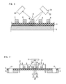
- the inspection detects the defective shape of the conductive pattern 4 by placing a reflection-type optical sensor 24 comprising a light emitting unit 22 and a light receiving unit 23 above the insulating layer 3 including the conductive pattern 4 in opposing relation, emitting sensing light from the light emitting unit 22 toward the insulating layer 3 including the conductive pattern 4 to irradiate it, and sensing the reflected light (sensing light) from the conductive pattern 4 by the light receiving unit 23, as shown in FIG. 6.
- the sensing light emitted from the light emitting unit 22 for irradiation transmits through the insulating layer 3 and is reflected by the metal supporting layer 2, the sensing light can be diffused in the metal supporting layer 2 since the specular gloss of the metal supporting layer 2 at an incidence angle of 45° is set not more than 500%. This can reduce erroneous determinations in the inspection and thereby improves inspection accuracy.
- the covering layer 11 is formed in the form of a rectangular frame-like shape to cover the relay leads 9 of the wires 6 and surround the mounting portion 10.
- the covering layer 11 is formed by a known method using a photosensitive solder resist or the like.
- the exposed portions of the wires 6, i.e., the inner leads 7 and the outer leads 8 are covered with a nickel plated layer and a gold plated layer.
- the nickel plated layer and the gold plated layer are formed by, e.g., nickel plating and gold plating, respectively.
- the opening 16 is formed in the portion of the metal supporting layer 2 which positionally corresponds to each of the conductive pattern formation regions 5, whereby the TAB tape carrier 1 is obtained.
- the portions of the metal supporting layer 2 which are individually overlapping the conductive pattern formation regions 5 are bored by wet etching (chemical etching).
- the etching is accomplished by covering the metal supporting layer 2 except for the portions thereof corresponding to the openings 16 with an etching resist, performing etching using a known etchant solution such as a ferric chloride solution, and then removing the etching resist. Thereafter, when the plurality of TAB tape carriers 1 are produced to be arranged in the widthwise direction of the metal supporting layer 2, the TAB tape carriers 1 are slit into individual strips.
- the slit portions of the metal supporting layer 2, which are located between the TAB tape carries 1, are simultaneously removed with the portions thereof corresponding to the openings 16.
- the specular gloss of the metal supporting layer 2 at an incidence angle of 45° is set not more than 500%, as described above, so that the defective shape of the conductive pattern 4 formed with a fine pitch is precisely and reliably detected.
- the TAB tape carrier 1 formed with the high-reliability conductive pattern 4 can be obtained.
- the electronic component 21 is mounted on the TAB tape carrier 1.
- the electronic component 21 and the surface (the surface on which the conductive pattern 4 is formed) of the mounting portion 10 of the insulating layer 3 are provided with respective marks 25 and 26 for alignment respectively, and a reflection-type optical sensor 29 comprising a light emitting unit 27 and a light receiving unit 28 is placed below the portion of the insulating layer 3 corresponding to the opening 16 in opposing relation, as shown in FIG. 7.
- Sensing light is emitted from the light emitting unit 27 toward each of the marks 25 and 26 to irradiate them and the sensing light transmitted through the insulating layer 3 of the mounting portion 10 and reflected by each of the marks 25 and 26 is received by the light receiving unit 28, so that alignment is performed by recognizing the marks 25 and 26.
- the specular gloss of the metal supporting layer 2 at an incidence angle of 45° is set not less than 150%, as described above. This setting prevents the haze value of the portion of the insulating layer 3 which is exposed from the opening 16 as a result of boring the metal supporting layer 2 from becoming excessively high and thereby allows excellent transmission of the sensing light for aligning the electronic component 21 through the insulating layer 3. As a result, the electronic component 21 can be mounted with accuracy.
- the haze value of the insulating layer 3 in the opening 16 is set in the range of 20 to 50% or preferably 20 to 40%.
- the haze value of the insulating layer 3 in the opening 16 is less than 20%, external light is reflected at the surface of the insulating layer 3, so that the problem of lower inspection accuracy occurs.
- the haze value of the insulating layer 3 in the opening 16 exceeds 50%, the transmission of the sensing light through the insulating layer 3 is inferior.
- the sensing light for aligning the electronic component 21 is excellently transmitted through the insulating layer 3. As a result, the electronic component 21 can be mounted with accuracy.
- the wired circuit board according to the present invention is not limited thereto.
- the present invention is also widely applicable to another wired circuit board.
- a metal supporting layer made of a stainless steel foil (SUS 304 with a thickness of 20 ⁇ m and a width of 250 mm) having a specular gloss of 200% at an incidence angle of 45° was prepared (see FIG. 4(a)).
- a solution of a polyamic acid resin was applied to the metal supporting layer, dried, and then heated to be cured to form an insulating layer made of a polyimide resin having a thickness of 25 ⁇ m (see FIG. 4(b)).
- a chromium thin film with a thickness of 300 ⁇ and a copper thin film with a thickness of 2000 ⁇ were successively formed on a surface of the insulating layer by a sputtering vapor deposition method, thereby forming a seed film (see FIG. 4(c)).
- the plating resist was dipped in an electrolytic copper sulfate plating solution and a surface of the portion of the seed film exposed from the plating resist was subjected to electrolytic copper plating at 2.5 A/dm 2 for abut 20 minutes, whereby a conductive pattern with a thickness of 10 ⁇ m was formed (see FIG. 5(f)).
- the conductive pattern was formed as a pattern of a plurality of wires arranged in mutually spaced-apart relation and comprising inner leads, outer leads, and relay leads which were formed integrally in continued relation.
- the pitch of the inner leads was 30 ⁇ m and the pitch of the outer leads was 100 ⁇ m.
- a photosensitive solder resist was formed to cover the respective relay leads of the wires and to surround each of the conductive pattern formation regions (see FIG. 5(i)). Then, the inner leads and the outer leads were covered by plating with nickel and gold.
- the metal supporting layer except for the portions thereof which positionally correspond to the conductive pattern formation regions and the slit formation regions was covered with an etching resist and etched by using a ferric chloride solution such that the openings and the slit portions between the individual TAB tape carriers were formed (see FIG. 5(j)), whereby the TAB tape carriers were obtained.
- the haze value of the portion of the insulating layer which was exposed from the opening was 40%.
- an IC chip was mounted on each of the obtained TAB tape carriers by using an IC mounting machine (inner lead bonder), while aligning the IC chip by a light reflection method using a position sensing apparatus (optical sensor).
- IC mounting machine inner lead bonder
- position sensing apparatus optical sensor
- TAB tape carriers were obtained in the same manner as in Example 1 except that a stainless steel foil having a specular gloss of 450% at an incidence angle of 45° was used. After inspecting the shape of the conductive patterns of the TAB tape carriers by a light reflection method, it was verified by the subsequent conduction test that there was no erroneous determination in the inspection.
- the haze value of the portion of the insulating layer exposed from the opening was 20%.
- TAB tape carriers were obtained in the same manner as in Example 1 except that a stainless steel foil having a specular gloss of 800% at an incidence angle of 45° was used. After inspecting the shape of the conductive patterns of the TAB tape carriers by a light reflection method, it was verified by the subsequent conduction test that, in products determined non-defective in the inspection, defective products with short-circuits were mixed.
- the haze value of the portion of the insulating layer exposed from the opening was 5%.
- TAB tape carriers were obtained in the same manner as in Example 1 except that a stainless steel foil having a specular gloss of 100% at an incidence angle of 45° was used. After inspecting the shape of the conductive patterns of the TAB tape carriers by a light-reflection method, it was verified by the subsequent conduction test that there was no erroneous determination in the inspection.
- the haze value of the portion of the insulating layer exposed from the opening was 60%.
Landscapes
- Engineering & Computer Science (AREA)
- Microelectronics & Electronic Packaging (AREA)
- Manufacturing & Machinery (AREA)
- Wire Bonding (AREA)
- Parts Printed On Printed Circuit Boards (AREA)
- Photometry And Measurement Of Optical Pulse Characteristics (AREA)
- Manufacturing Of Printed Circuit Boards (AREA)
- Investigating Materials By The Use Of Optical Means Adapted For Particular Applications (AREA)
- Supply And Installment Of Electrical Components (AREA)
Applications Claiming Priority (1)
| Application Number | Priority Date | Filing Date | Title |
|---|---|---|---|
| JP2005329010A JP2007134658A (ja) | 2005-11-14 | 2005-11-14 | 配線回路基板および配線回路基板を製造し電子部品を実装する方法 |
Publications (2)
| Publication Number | Publication Date |
|---|---|
| EP1786247A2 true EP1786247A2 (fr) | 2007-05-16 |
| EP1786247A3 EP1786247A3 (fr) | 2008-11-19 |
Family
ID=37745876
Family Applications (1)
| Application Number | Title | Priority Date | Filing Date |
|---|---|---|---|
| EP06023447A Withdrawn EP1786247A3 (fr) | 2005-11-14 | 2006-11-10 | Panneau à circuit et procédé de fabrication d'un panneau à circuit et de montage d'un composant électronique sur celui-ci |
Country Status (6)
| Country | Link |
|---|---|
| US (2) | US7561434B2 (fr) |
| EP (1) | EP1786247A3 (fr) |
| JP (1) | JP2007134658A (fr) |
| KR (1) | KR20070051723A (fr) |
| CN (1) | CN100552936C (fr) |
| TW (1) | TW200725769A (fr) |
Cited By (3)
| Publication number | Priority date | Publication date | Assignee | Title |
|---|---|---|---|---|
| EP2086297A2 (fr) | 2008-01-31 | 2009-08-05 | Nitto Denko Corporation | Carte à circuit imprimé et procédé de fabrication correspondant |
| EP2086296A2 (fr) | 2008-01-31 | 2009-08-05 | Nitto Denko Corporation | Carte à circuit imprimé et procédé de fabrication correspondant |
| WO2009115796A1 (fr) * | 2008-03-17 | 2009-09-24 | Dek International Gmbh | Système d'imagerie et procédé d'alignement |
Families Citing this family (16)
| Publication number | Priority date | Publication date | Assignee | Title |
|---|---|---|---|---|
| JP5095460B2 (ja) * | 2008-01-17 | 2012-12-12 | シャープ株式会社 | 半導体装置および表示装置 |
| KR20100006448A (ko) * | 2008-07-09 | 2010-01-19 | 엘지전자 주식회사 | 이동식 저장 장치 |
| TWI439945B (zh) * | 2008-11-14 | 2014-06-01 | 凸版印刷股份有限公司 | 非接觸型ic標籤及物品 |
| JP5334617B2 (ja) * | 2009-02-17 | 2013-11-06 | 日東電工株式会社 | 配線回路基板の製造方法 |
| JP5511597B2 (ja) * | 2010-09-06 | 2014-06-04 | 日東電工株式会社 | 配線回路基板の製造方法 |
| KR101148099B1 (ko) * | 2010-10-01 | 2012-05-23 | 엘지이노텍 주식회사 | 탭 테이프 및 그 제조방법 |
| WO2012137926A1 (fr) * | 2011-04-07 | 2012-10-11 | 日産自動車株式会社 | Dispositif et procédé de stratification d'électrodes |
| TWI612691B (zh) * | 2013-09-02 | 2018-01-21 | 古河電氣工業股份有限公司 | 用於光半導體裝置之引線框架用之基體及其製造方法、用有此之用於光半導體裝置之引線框架及其製造方法、及光半導體裝置 |
| JP5695253B1 (ja) * | 2014-06-23 | 2015-04-01 | 株式会社Shカッパープロダクツ | 銅張積層板および該銅張積層板を用いたフレキシブルプリント配線板 |
| JP5732181B1 (ja) * | 2015-02-05 | 2015-06-10 | 株式会社Shカッパープロダクツ | 銅張積層板および該銅張積層板を用いたフレキシブルプリント配線板 |
| JP7101512B2 (ja) * | 2018-03-28 | 2022-07-15 | Fdk株式会社 | 回路基板及びその製造方法 |
| JP7263204B2 (ja) | 2019-10-16 | 2023-04-24 | 日東電工株式会社 | 配線回路基板の製造方法 |
| TWI692278B (zh) * | 2019-11-01 | 2020-04-21 | 頎邦科技股份有限公司 | 軟性線路板 |
| TWI717886B (zh) * | 2019-11-01 | 2021-02-01 | 頎邦科技股份有限公司 | 軟性線路板 |
| TWI744805B (zh) * | 2020-02-24 | 2021-11-01 | 頎邦科技股份有限公司 | 電路板 |
| CN115279951B (zh) * | 2020-03-27 | 2025-04-08 | 古河电气工业株式会社 | 印刷配线板用表面处理铜箔、以及使用其的印刷配线板用覆铜层叠板和印刷配线板 |
Family Cites Families (14)
| Publication number | Priority date | Publication date | Assignee | Title |
|---|---|---|---|---|
| US4806432A (en) * | 1985-11-21 | 1989-02-21 | Shin-Etsu Chemical Co., Ltd. | Copper-foiled laminated sheet for flexible printed circuit board |
| JPH04291109A (ja) * | 1991-03-20 | 1992-10-15 | Fujitsu Ltd | 高さ計測装置 |
| JPH0526821A (ja) * | 1991-07-26 | 1993-02-02 | Fujitsu Ltd | 外観検査装置 |
| US5249576A (en) * | 1991-10-24 | 1993-10-05 | Boc Health Care, Inc. | Universal pulse oximeter probe |
| JPH05249047A (ja) * | 1992-03-04 | 1993-09-28 | Fujitsu Ltd | パターン検査装置 |
| JP2000332062A (ja) * | 1999-05-18 | 2000-11-30 | Shindo Denshi Kogyo Kk | Tab用薄膜テープキャリアの製造法 |
| JP3555502B2 (ja) * | 1999-05-27 | 2004-08-18 | 日立電線株式会社 | Cof用tabテープキャリアの製造方法 |
| JP2002299391A (ja) * | 2001-04-03 | 2002-10-11 | Teijin Ltd | Tabリードテープ用ポリエステルフィルム |
| JP2003309336A (ja) * | 2002-04-15 | 2003-10-31 | Toray Ind Inc | フレキシブルプリント基板用積層板およびフレキシブルプリント基板 |
| US6984456B2 (en) * | 2002-05-13 | 2006-01-10 | Mitsui Mining & Smelting Co., Ltd. | Flexible printed wiring board for chip-on flexibles |
| TWI298988B (en) * | 2002-07-19 | 2008-07-11 | Ube Industries | Copper-clad laminate |
| JP2004098659A (ja) * | 2002-07-19 | 2004-04-02 | Ube Ind Ltd | 銅張積層板及びその製造方法 |
| JP3694286B2 (ja) * | 2002-10-08 | 2005-09-14 | 日東電工株式会社 | Tab用テープキャリア |
| JP2005333028A (ja) * | 2004-05-20 | 2005-12-02 | Nitto Denko Corp | 配線回路基板 |
-
2005
- 2005-11-14 JP JP2005329010A patent/JP2007134658A/ja active Pending
-
2006
- 2006-11-03 TW TW095140700A patent/TW200725769A/zh unknown
- 2006-11-10 EP EP06023447A patent/EP1786247A3/fr not_active Withdrawn
- 2006-11-13 CN CNB2006101464776A patent/CN100552936C/zh not_active Expired - Fee Related
- 2006-11-13 US US11/595,984 patent/US7561434B2/en not_active Expired - Fee Related
- 2006-11-14 KR KR1020060112094A patent/KR20070051723A/ko not_active Withdrawn
-
2009
- 2009-06-03 US US12/457,183 patent/US20090242506A1/en not_active Abandoned
Cited By (9)
| Publication number | Priority date | Publication date | Assignee | Title |
|---|---|---|---|---|
| EP2086297A2 (fr) | 2008-01-31 | 2009-08-05 | Nitto Denko Corporation | Carte à circuit imprimé et procédé de fabrication correspondant |
| EP2086296A2 (fr) | 2008-01-31 | 2009-08-05 | Nitto Denko Corporation | Carte à circuit imprimé et procédé de fabrication correspondant |
| EP2086297A3 (fr) * | 2008-01-31 | 2010-05-26 | Nitto Denko Corporation | Carte à circuit imprimé et procédé de fabrication correspondant |
| EP2086296A3 (fr) * | 2008-01-31 | 2010-05-26 | Nitto Denko Corporation | Carte à circuit imprimé et procédé de fabrication correspondant |
| US8097814B2 (en) | 2008-01-31 | 2012-01-17 | Nitto Denko Corporation | Printed circuit board and method of manufacturing the same |
| US8102664B2 (en) | 2008-01-31 | 2012-01-24 | Nitto Denko Corporation | Printed circuit board and method of manufacturing the same |
| TWI453870B (zh) * | 2008-01-31 | 2014-09-21 | 日東電工股份有限公司 | 配線電路基板及其製造方法 |
| KR101477818B1 (ko) * | 2008-01-31 | 2014-12-30 | 닛토덴코 가부시키가이샤 | 배선 회로 기판 및 그 제조 방법 |
| WO2009115796A1 (fr) * | 2008-03-17 | 2009-09-24 | Dek International Gmbh | Système d'imagerie et procédé d'alignement |
Also Published As
| Publication number | Publication date |
|---|---|
| US20090242506A1 (en) | 2009-10-01 |
| US20070108631A1 (en) | 2007-05-17 |
| US7561434B2 (en) | 2009-07-14 |
| CN100552936C (zh) | 2009-10-21 |
| CN1967831A (zh) | 2007-05-23 |
| KR20070051723A (ko) | 2007-05-18 |
| TW200725769A (en) | 2007-07-01 |
| JP2007134658A (ja) | 2007-05-31 |
| EP1786247A3 (fr) | 2008-11-19 |
Similar Documents
| Publication | Publication Date | Title |
|---|---|---|
| US20090242506A1 (en) | Wired circuit board and method for manufacturing wired circuit board and mounting electronic component thereon | |
| EP1599076A1 (fr) | Panneau à circuit | |
| US8477507B2 (en) | Suspension board assembly sheet with circuits and method for manufacturing the same | |
| TWI417006B (zh) | 配線電路基板的製造方法及檢查方法 | |
| US9313880B2 (en) | Printed circuit board, printed circuit board assembly sheet and method of manufacturing the same | |
| US8037597B2 (en) | Manufacturing method of tape carrier for TAB | |
| CN109195313A (zh) | 一种新型背钻测试孔制作方法 | |
| KR20090013805A (ko) | 플렉서블 프린트 배선 기판의 배선 패턴 검사 방법 및 검사장치 | |
| CN112638043B (zh) | 飞尾式结构的刚挠结合板制作方法 | |
| US7358619B2 (en) | Tape carrier for TAB | |
| US6953989B2 (en) | Film carrier tape for mounting electronic devices thereon and final defect marking method using the same | |
| JP2000223840A (ja) | ビルドアップ多層配線板の製造方法 | |
| CN118549437A (zh) | 柔性线路板中不良盲孔的检测方法 | |
| JP2011171373A (ja) | 配線回路基板の検査方法および製造方法 | |
| TWI239800B (en) | Manufacture method of flexible printed circuit board (PCB) | |
| KR20050055991A (ko) | 마이크로 비아홀의 테스트 쿠폰이 구비된 인쇄회로기판 및그 제조 방법 | |
| JPH11191668A (ja) | 集合基板およびその各分割部分の良否判別方法 | |
| CN108650795B (zh) | 封装基板的打码方法、加工方法及封装基板 | |
| CN121793272A (zh) | 线路板的金手指加工方法及线路板 | |
| JP2004281827A (ja) | 配線板の製造方法 | |
| JP3789383B2 (ja) | 電子部品実装用フィルムキャリアテープの検査方法 | |
| JP4762800B2 (ja) | 配線回路基板の製造方法 | |
| CN116367444A (zh) | 一种厚铜板外层蚀刻的蚀刻补偿方法 | |
| CN109121312A (zh) | 一种基于过孔可精确调节埋阻值的方法 | |
| CN121645721A (zh) | 一种目视化管控涨缩和层偏量的方法 |
Legal Events
| Date | Code | Title | Description |
|---|---|---|---|
| PUAI | Public reference made under article 153(3) epc to a published international application that has entered the european phase |
Free format text: ORIGINAL CODE: 0009012 |
|
| AK | Designated contracting states |
Kind code of ref document: A2 Designated state(s): AT BE BG CH CY CZ DE DK EE ES FI FR GB GR HU IE IS IT LI LT LU LV MC NL PL PT RO SE SI SK TR |
|
| AX | Request for extension of the european patent |
Extension state: AL BA HR MK YU |
|
| PUAL | Search report despatched |
Free format text: ORIGINAL CODE: 0009013 |
|
| AK | Designated contracting states |
Kind code of ref document: A3 Designated state(s): AT BE BG CH CY CZ DE DK EE ES FI FR GB GR HU IE IS IT LI LT LU LV MC NL PL PT RO SE SI SK TR |
|
| AX | Request for extension of the european patent |
Extension state: AL BA HR MK RS |
|
| 17P | Request for examination filed |
Effective date: 20090409 |
|
| AKX | Designation fees paid |
Designated state(s): DE FR GB |
|
| STAA | Information on the status of an ep patent application or granted ep patent |
Free format text: STATUS: THE APPLICATION HAS BEEN WITHDRAWN |
|
| 18W | Application withdrawn |
Effective date: 20100901 |