EP1788546A2 - Appareil et procédé de commande d'un affichage à plasma - Google Patents
Appareil et procédé de commande d'un affichage à plasma Download PDFInfo
- Publication number
- EP1788546A2 EP1788546A2 EP06251141A EP06251141A EP1788546A2 EP 1788546 A2 EP1788546 A2 EP 1788546A2 EP 06251141 A EP06251141 A EP 06251141A EP 06251141 A EP06251141 A EP 06251141A EP 1788546 A2 EP1788546 A2 EP 1788546A2
- Authority
- EP
- European Patent Office
- Prior art keywords
- voltage
- bias voltage
- electrode
- sustain
- period
- Prior art date
- Legal status (The legal status is an assumption and is not a legal conclusion. Google has not performed a legal analysis and makes no representation as to the accuracy of the status listed.)
- Granted
Links
- 238000000034 method Methods 0.000 title claims abstract description 17
- 238000011084 recovery Methods 0.000 claims abstract description 31
- 239000003990 capacitor Substances 0.000 claims description 18
- 238000013459 approach Methods 0.000 claims description 4
- 230000003405 preventing effect Effects 0.000 abstract description 4
- 238000010586 diagram Methods 0.000 description 4
- 230000000630 rising effect Effects 0.000 description 4
- 230000002459 sustained effect Effects 0.000 description 3
- 230000004888 barrier function Effects 0.000 description 2
- 238000010276 construction Methods 0.000 description 2
- 230000003247 decreasing effect Effects 0.000 description 2
- CPBQJMYROZQQJC-UHFFFAOYSA-N helium neon Chemical compound [He].[Ne] CPBQJMYROZQQJC-UHFFFAOYSA-N 0.000 description 2
- AFAUWLCCQOEICZ-UHFFFAOYSA-N helium xenon Chemical compound [He].[Xe] AFAUWLCCQOEICZ-UHFFFAOYSA-N 0.000 description 2
- 239000000758 substrate Substances 0.000 description 2
- OAICVXFJPJFONN-UHFFFAOYSA-N Phosphorus Chemical compound [P] OAICVXFJPJFONN-UHFFFAOYSA-N 0.000 description 1
- 230000015556 catabolic process Effects 0.000 description 1
- 238000006731 degradation reaction Methods 0.000 description 1
- 239000011521 glass Substances 0.000 description 1
- 239000011261 inert gas Substances 0.000 description 1
- 239000011159 matrix material Substances 0.000 description 1
- 238000012986 modification Methods 0.000 description 1
- 230000004048 modification Effects 0.000 description 1
- 230000005855 radiation Effects 0.000 description 1
Images




Classifications
-
- G—PHYSICS
- G09—EDUCATION; CRYPTOGRAPHY; DISPLAY; ADVERTISING; SEALS
- G09G—ARRANGEMENTS OR CIRCUITS FOR CONTROL OF INDICATING DEVICES USING STATIC MEANS TO PRESENT VARIABLE INFORMATION
- G09G3/00—Control arrangements or circuits, of interest only in connection with visual indicators other than cathode-ray tubes
- G09G3/20—Control arrangements or circuits, of interest only in connection with visual indicators other than cathode-ray tubes for presentation of an assembly of a number of characters, e.g. a page, by composing the assembly by combination of individual elements arranged in a matrix no fixed position being assigned to or needed to be assigned to the individual characters or partial characters
- G09G3/22—Control arrangements or circuits, of interest only in connection with visual indicators other than cathode-ray tubes for presentation of an assembly of a number of characters, e.g. a page, by composing the assembly by combination of individual elements arranged in a matrix no fixed position being assigned to or needed to be assigned to the individual characters or partial characters using controlled light sources
- G09G3/28—Control arrangements or circuits, of interest only in connection with visual indicators other than cathode-ray tubes for presentation of an assembly of a number of characters, e.g. a page, by composing the assembly by combination of individual elements arranged in a matrix no fixed position being assigned to or needed to be assigned to the individual characters or partial characters using controlled light sources using luminous gas-discharge panels, e.g. plasma panels
- G09G3/288—Control arrangements or circuits, of interest only in connection with visual indicators other than cathode-ray tubes for presentation of an assembly of a number of characters, e.g. a page, by composing the assembly by combination of individual elements arranged in a matrix no fixed position being assigned to or needed to be assigned to the individual characters or partial characters using controlled light sources using luminous gas-discharge panels, e.g. plasma panels using AC panels
- G09G3/296—Driving circuits for producing the waveforms applied to the driving electrodes
- G09G3/2965—Driving circuits for producing the waveforms applied to the driving electrodes using inductors for energy recovery
-
- G—PHYSICS
- G09—EDUCATION; CRYPTOGRAPHY; DISPLAY; ADVERTISING; SEALS
- G09G—ARRANGEMENTS OR CIRCUITS FOR CONTROL OF INDICATING DEVICES USING STATIC MEANS TO PRESENT VARIABLE INFORMATION
- G09G3/00—Control arrangements or circuits, of interest only in connection with visual indicators other than cathode-ray tubes
- G09G3/20—Control arrangements or circuits, of interest only in connection with visual indicators other than cathode-ray tubes for presentation of an assembly of a number of characters, e.g. a page, by composing the assembly by combination of individual elements arranged in a matrix no fixed position being assigned to or needed to be assigned to the individual characters or partial characters
- G09G3/22—Control arrangements or circuits, of interest only in connection with visual indicators other than cathode-ray tubes for presentation of an assembly of a number of characters, e.g. a page, by composing the assembly by combination of individual elements arranged in a matrix no fixed position being assigned to or needed to be assigned to the individual characters or partial characters using controlled light sources
- G09G3/28—Control arrangements or circuits, of interest only in connection with visual indicators other than cathode-ray tubes for presentation of an assembly of a number of characters, e.g. a page, by composing the assembly by combination of individual elements arranged in a matrix no fixed position being assigned to or needed to be assigned to the individual characters or partial characters using controlled light sources using luminous gas-discharge panels, e.g. plasma panels
- G09G3/288—Control arrangements or circuits, of interest only in connection with visual indicators other than cathode-ray tubes for presentation of an assembly of a number of characters, e.g. a page, by composing the assembly by combination of individual elements arranged in a matrix no fixed position being assigned to or needed to be assigned to the individual characters or partial characters using controlled light sources using luminous gas-discharge panels, e.g. plasma panels using AC panels
- G09G3/296—Driving circuits for producing the waveforms applied to the driving electrodes
-
- G—PHYSICS
- G09—EDUCATION; CRYPTOGRAPHY; DISPLAY; ADVERTISING; SEALS
- G09G—ARRANGEMENTS OR CIRCUITS FOR CONTROL OF INDICATING DEVICES USING STATIC MEANS TO PRESENT VARIABLE INFORMATION
- G09G3/00—Control arrangements or circuits, of interest only in connection with visual indicators other than cathode-ray tubes
- G09G3/20—Control arrangements or circuits, of interest only in connection with visual indicators other than cathode-ray tubes for presentation of an assembly of a number of characters, e.g. a page, by composing the assembly by combination of individual elements arranged in a matrix no fixed position being assigned to or needed to be assigned to the individual characters or partial characters
- G09G3/22—Control arrangements or circuits, of interest only in connection with visual indicators other than cathode-ray tubes for presentation of an assembly of a number of characters, e.g. a page, by composing the assembly by combination of individual elements arranged in a matrix no fixed position being assigned to or needed to be assigned to the individual characters or partial characters using controlled light sources
- G09G3/28—Control arrangements or circuits, of interest only in connection with visual indicators other than cathode-ray tubes for presentation of an assembly of a number of characters, e.g. a page, by composing the assembly by combination of individual elements arranged in a matrix no fixed position being assigned to or needed to be assigned to the individual characters or partial characters using controlled light sources using luminous gas-discharge panels, e.g. plasma panels
- G09G3/288—Control arrangements or circuits, of interest only in connection with visual indicators other than cathode-ray tubes for presentation of an assembly of a number of characters, e.g. a page, by composing the assembly by combination of individual elements arranged in a matrix no fixed position being assigned to or needed to be assigned to the individual characters or partial characters using controlled light sources using luminous gas-discharge panels, e.g. plasma panels using AC panels
- G09G3/291—Control arrangements or circuits, of interest only in connection with visual indicators other than cathode-ray tubes for presentation of an assembly of a number of characters, e.g. a page, by composing the assembly by combination of individual elements arranged in a matrix no fixed position being assigned to or needed to be assigned to the individual characters or partial characters using controlled light sources using luminous gas-discharge panels, e.g. plasma panels using AC panels controlling the gas discharge to control a cell condition, e.g. by means of specific pulse shapes
- G09G3/292—Control arrangements or circuits, of interest only in connection with visual indicators other than cathode-ray tubes for presentation of an assembly of a number of characters, e.g. a page, by composing the assembly by combination of individual elements arranged in a matrix no fixed position being assigned to or needed to be assigned to the individual characters or partial characters using controlled light sources using luminous gas-discharge panels, e.g. plasma panels using AC panels controlling the gas discharge to control a cell condition, e.g. by means of specific pulse shapes for reset discharge, priming discharge or erase discharge occurring in a phase other than addressing
- G09G3/2927—Details of initialising
-
- G—PHYSICS
- G09—EDUCATION; CRYPTOGRAPHY; DISPLAY; ADVERTISING; SEALS
- G09G—ARRANGEMENTS OR CIRCUITS FOR CONTROL OF INDICATING DEVICES USING STATIC MEANS TO PRESENT VARIABLE INFORMATION
- G09G2320/00—Control of display operating conditions
- G09G2320/02—Improving the quality of display appearance
- G09G2320/0238—Improving the black level
-
- G—PHYSICS
- G09—EDUCATION; CRYPTOGRAPHY; DISPLAY; ADVERTISING; SEALS
- G09G—ARRANGEMENTS OR CIRCUITS FOR CONTROL OF INDICATING DEVICES USING STATIC MEANS TO PRESENT VARIABLE INFORMATION
- G09G2330/00—Aspects of power supply; Aspects of display protection and defect management
- G09G2330/02—Details of power systems and of start or stop of display operation
- G09G2330/028—Generation of voltages supplied to electrode drivers in a matrix display other than LCD
Definitions
- the present invention relates to an apparatus and method for driving a plasma display. It more particularly relates to an apparatus and method for driving a plasma display capable of preventing an erroneous discharge by applying a voltage that is about 1/2 of a sustain voltage to a sustain electrode during a set-up period, and precisely and uniformly controlling wall charges during the set-up period.
- a conventional plasma display apparatus is constructed such that barrier ribs formed between upper and lower glass substrates constitute a unit cell, and when an inert gas such as helium-xenon (He-Xe), helium-neon (He-Ne), or the like, in each cell is discharged by a high frequency voltage, vacuum ultraviolet radiation is generated to cause phosphor formed between the barrier ribs to emit visible light, to thereby allow images to be displayed.
- an inert gas such as helium-xenon (He-Xe), helium-neon (He-Ne), or the like
- the plasma display apparatus can be easily manufactured. Due to its thin outer appearance and low power consumption it is receiving much attention as a next-generation display apparatus.
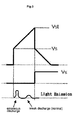
- FIG. 1 is a driving waveform view of an apparatus for driving a plasma display in accordance with the prior art
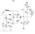
- FIG. 2 is a circuit diagram showing the construction of an apparatus for driving a scan electrode of the plasma display in accordance with the prior art
- FIG. 3 is an exemplary view showing a problem of the apparatus for driving the plasma display in accordance with the prior art.
- a plurality of first and second electrodes are formed in parallel on a front panel and a plurality of third electrodes are formed in a direction perpendicular to the first and second electrodes on a rear panel.
- the electrodes are arranged in a matrix form, forming cells, and a discharge occurs in each cell by a driving waveform.
- the first electrodes are scan electrodes (Y) and the second electrodes are sustain electrodes (Z).
- the third electrodes are address electrodes.
- driving waveforms as shown in FIG. 1 are applied to the scan electrodes and the sustain during one sub-field period.
- One sub-field is divided into a reset period, an address period and a sustain period, and the reset period is divided into a set-up period and a set-down period.
- the voltage applied to the scan electrode is gradually increased to increase the amount of wall charges, and during the set-down period, the voltage is gradually decreased to reduce the generated wall charges to a certain amount without a discharge.
- a set-up waveform applied to the scan electrode becomes a ramp up (rising) waveform during the set-up period and becomes a ramp down (falling) waveform during the set-down period.
- the set-up waveform can be ramp-increased by sustaining its slope from an initial ground level, but since a portion that requires a reset discharge occurs at or above a certain high level voltage, it is not necessary to supply a waveform with a steep slope from the beginning.
- a circuit is constructed and operated such that the set-up waveform can be ramp-increased by using a sustain voltage (Vs) as a-base voltage.
- Vs sustain voltage
- an energy recovery unit and a sustain voltage apply unit 10 are common parts which are also provided in an apparatus for driving a sustain electrode.
- the sustain electrode (Z) is sustained by a ground voltage, and a ramp up waveform, which rises from the sustain voltage (Vs), is applied to the scan electrode (Y).
- the voltage difference between the scan electrode and the sustain electrode may cause an erroneous discharge, which results in a problem of degradation of the contrast of an image or the picture quality.
- the present invention seeks to provide an improved plasma display apparatus.
- Embodiments of the present invention can provide an apparatus and method for driving a plasma display which are capable of preventing occurrence of an erroneous discharge by reducing a difference between a voltage applied to a scan electrode and a voltage applied to a sustain electrode during a set-up period by using an existing driving circuit without constructing an additional circuit device.
- an apparatus for driving a plasma display including first and second electrode driving units for applying a drive signal to first and second electrodes formed in parallel on a front panel, wherein the second electrode driving unit is arranged to apply a first bias voltage having a certain size not greater than a sustain voltage to the second electrode during a set-up period.
- the first bias voltage may have a value of about a half of the sustain voltage.
- the second electrode driving unit may include an energy recovery unit for recovering energy stored in a panel, and may apply an output voltage of the energy recovery unit as the first bias voltage.
- the first bias voltage may be a waveform which approaches a value of about a half of the sustain voltage as free resonance is generated.
- the first bias voltage may be applied substantially simultaneously with a drive voltage which is applied to the first electrode when the set-up period starts.
- an apparatus for driving a plasma display including: first and second electrode driving units for applying a drive signal to first and second electrodes formed in parallel on a front panel, wherein the second electrode driving unit is arranged to apply a first bias voltage to the second electrode during a set-up period and a second bias voltage during an address period, and a difference between the first and second bias voltages is not substantially greater than a half of a sustain voltage.
- Another aspect of the invention provides a method for driving a plasma display in which first and second electrodes are formed in parallel on a front panel and an energy recovery unit recovers/re-supplies energy stored in the panel through the first and second electrodes, including: applying a gradually increased voltage to the first electrode during a set-up period; and applying a first bias voltage having a value not greater than a sustain voltage to the second electrode during the set-up period.
- a plasma display apparatus includes first and second electrodes formed in parallel on an upper substrate, first and second electrode driving units for applying a drive signal to the first and second electrodes, and an energy recovery unit for recovering/re-supplying energy stored in a panel.
- the first electrode may be a scan electrode and the second electrode may be a sustain electrode.
- the first electrode driving unit may apply a driving waveform to the scan electrode of the plasma display panel
- the second electrode driving unit may apply a driving waveform which forms or erases wall charges or generates a discharge in unison with the driving waveform applied to the first electrode
- the applied driving waveforms may be divided into a reset period, an address period and a sustain period, respectively, per each sub-field, and the reset period may be divided into a set-up period and a set-down period.
- a voltage applied to the first electrode may be gradually increased to increase the amount of wall charges within a discharge cell, and during the set-down period, the voltage may be gradually decreased to reduce the generated wall charges to a certain amount without a discharge.
- the first electrode driving unit may apply a waveform which is ramp-increased from a certain base voltage up to a set-up voltage to the scan electrode during the set-up period.
- the first electrode driving unit may apply the waveform which rises from the voltage having the same size as the ground voltage or the sustain voltage to the set-up voltage to the first electrode.
- the second electrode driving unit may apply a first bias voltage (Vb1) having a certain size smaller than the sustain voltage to the second electrode (sustain electrode) during the set-up period.
- Vb1 a first bias voltage having a certain size smaller than the sustain voltage
- a plasma display apparatus in accordance with a first embodiment is characterized in that the first bias voltage (Vb1) has the size of about a half of the sustain voltage (Vs).
- the voltage of about the half (Vs/2) of the sustain voltage can be applied by using an output of the energy recovery unit.
- FIG. 4 is a circuit diagram of a second electrode driving unit. As shown in FIG. 4, the second electrode driving unit includes an energy recovery unit 100 and a sustain voltage applying unit 200.
- the energy recovery unit 100 includes a source capacitor (Cs) having one end connected to ground, an inductor (L1) connected with a contact node (Vz) of the sustain voltage applying unit 200, first and second switching elements (S1,S2) connected in parallel between the inductor (Ll) and the source capacitor (Cs), and a plurality of diodes connected in series with the switching elements.
- Cs source capacitor
- L1 inductor
- Vz contact node
- S1,S2 first and second switching elements
- the sustain voltage applying unit 200 includes a sustain voltage source (Vs) and third and fourth switching elements (S3 and S4) connected to the voltage source, and one end of the inductor (Ll) of the energy recovery unit 100 is connected to a contact node (Vz) of the third and fourth switching elements (S3 and S4).
- a panel capacitor is connected to the contact node (Vz), so that resonance occurs between the panel capacitor and the inductor (L1).
- Charge at a potential of about half the voltage (Vs/2) of the sustain voltage is stored in the source capacitor (Cs) of the energy recovery unit 100, and by controlling the plurality of switching elements provided in the second electrode driving unit, the voltage stored in the source capacitor (Cs) can be applied as the first bias voltage (Vb1) during the set-up period.
- the third switching element (S3) is sustained in an OFF state and so does the fourth switching element (S4).
- a waveform which rises at a certain slope up to a set-up voltage (Vst) by using the sustain voltage (Vs) or the ground voltage as a base voltage is applied to the first electrode.
- the maximum potential becomes higher than half the voltage (Vs/2) of the sustain voltage, further reducing the potential difference between the first and second electrodes, so occurrence of the erroneous discharge can be more effectively prevented.
- the driving waveform applied to the second electrode gradually approaches half the voltage (Vs/2) of the sustain voltage.
- the sustain voltage (Vs) is applied by the sustain voltage applying unit 200 during the set-down period and the address period likewise as in the prior art.
- a voltage lower than the sustain voltage can be applied as the first bias voltage (Vb1) during the set-up period and the address period.
- a plasma display apparatus in accordance with another embodiment includes first and second electrode driving units for applying driving waveforms to first and second electrodes formed in parallel on a front panel, in which the first electrode driving unit applies a first bias voltage (Vb1) to the second electrode during the set-up period and applies a second bias voltage (Vb2) during the address period, and in this case, the difference between the first and second bias voltages is not substantially greater than a half of the sustain voltage.
- Vb1 first bias voltage
- Vb2 second bias voltage
- the first bias voltage is applied by using an additional power source.
- the difference between the first and second bias voltages (Vb1 and Vb2) needs to be controlled to be substantially smaller than half of the sustain voltage.
- the potential difference between a ramp waveform applied to the first electrode and the first bias voltage can be reduced as in the first embodiment, so occurrence of an erroneous discharge can be prevented.
- Vb1 and Vb2 If the difference between the first and second bias voltages (Vb1 and Vb2) exceeds about half (Vs/2) of the sustain voltage, the potential difference between the voltage applied at the initial stage of the set-up period and the first bias voltage (Vb1) applied to the second electrode would be increased to generate the erroneous discharge.
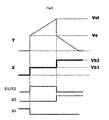
- FIG. 7 is a view showing time points at which a driving waveform is applied in the apparatus for driving a plasma display.
- the first bias voltage (Vb1) is applied to the second electrode at a time point (t2), or as shown in FIG. 5, the first bias voltage (Vb1) is simultaneously applied to the second electrode in synchronization with the time point when the ramp waveform is applied to the first electrode.
- Vb1 the first bias voltage
- FIG. 8 shows a result of a waveform obtained from experimentation as outputted to an oscilloscope.
- a method for driving a plasma display includes a first step of applying a gradually increased voltage to the scan electrode during the set-up period of a driving waveform applied to the plasma display panel, and a second step of applying the first bias voltage (Vb1) having the size not greater than the sustain voltage to the sustain electrode during the set-up period.
- a voltage having the substantially same size as the sustain voltage or a voltage which is gradually increased up to the set-up voltage from the ground voltage is applied.
- the first bias voltage (Vb1) in the second step has the size of about half of the sustain voltage.
- Vb1 a different voltage value is used as the first bias voltage (Vb1), an additional voltage source must be provided, but in the case of using half the voltage (Vs/2) of the sustain voltage, the output value of the energy recovery unit 100 can be used, so it is not necessary to construct an additional device.
- the output value of the energy recovery unit 100 is a voltage value stored in the source capacitor of the energy recover unit 100.
- the first bias voltage (Vb1) is the output voltage of the energy recovery unit 100.
- the recovery voltage value stored in the source capacitor of the energy recovery unit 100 is half (Vs/2) of the sustain voltage.
- Resonance takes place between the inductor (L1 in FIG. 4) of the energy recovery unit 100 and the panel capacitor according to the switching operation, and at the time point when the switching operation is performed, the resonance waveform is generated.
- a set-up waveform is applied to the scan electrode and, at the same time, the first bias voltage (Vb1) is applied to the sustain electrode.
- the first bias voltage (Vb1) starts to be applied, resonance takes place, and thus, the first bias voltage (Vb1) is gradually converges towards a level of about half of the sustain voltage.
- the potential difference between the first and second electrodes can be reduced by using the free resonance waveform which is generated at the initial stage of the set-up period, to thereby reduce an erroneous discharge.
- the second bias voltage has the substantially same size as the sustain voltage.
Landscapes
- Engineering & Computer Science (AREA)
- Physics & Mathematics (AREA)
- Power Engineering (AREA)
- Plasma & Fusion (AREA)
- Computer Hardware Design (AREA)
- General Physics & Mathematics (AREA)
- Theoretical Computer Science (AREA)
- Control Of Indicators Other Than Cathode Ray Tubes (AREA)
- Control Of Gas Discharge Display Tubes (AREA)
- Transforming Electric Information Into Light Information (AREA)
Applications Claiming Priority (1)
| Application Number | Priority Date | Filing Date | Title |
|---|---|---|---|
| KR1020050103126A KR100743708B1 (ko) | 2005-10-31 | 2005-10-31 | 플라즈마 디스플레이 장치 |
Publications (3)
| Publication Number | Publication Date |
|---|---|
| EP1788546A2 true EP1788546A2 (fr) | 2007-05-23 |
| EP1788546A3 EP1788546A3 (fr) | 2009-04-01 |
| EP1788546B1 EP1788546B1 (fr) | 2011-09-07 |
Family
ID=37983869
Family Applications (1)
| Application Number | Title | Priority Date | Filing Date |
|---|---|---|---|
| EP06251141A Expired - Lifetime EP1788546B1 (fr) | 2005-10-31 | 2006-03-02 | Appareil et procédé de commande d'un affichage à plasma |
Country Status (5)
| Country | Link |
|---|---|
| US (1) | US20070097032A1 (fr) |
| EP (1) | EP1788546B1 (fr) |
| JP (1) | JP2007128021A (fr) |
| KR (1) | KR100743708B1 (fr) |
| CN (1) | CN1959782A (fr) |
Cited By (1)
| Publication number | Priority date | Publication date | Assignee | Title |
|---|---|---|---|---|
| EP2113902A3 (fr) * | 2008-04-30 | 2010-02-24 | Samsung SDI Co., Ltd. | Dispositif à écran plasma et procédé de commande associé |
Families Citing this family (2)
| Publication number | Priority date | Publication date | Assignee | Title |
|---|---|---|---|---|
| TW200733043A (en) * | 2006-02-06 | 2007-09-01 | Matsushita Electric Industrial Co Ltd | Plasma display apparatus and driving method of plasma display panel |
| WO2009069175A1 (fr) * | 2007-11-27 | 2009-06-04 | Hitachi, Ltd. | Dispositif d'affichage à plasma |
Citations (2)
| Publication number | Priority date | Publication date | Assignee | Title |
|---|---|---|---|---|
| US20030107532A1 (en) | 2001-12-07 | 2003-06-12 | Lg Electronics Inc. | Method of driving plasma display panel |
| US6803888B1 (en) | 1999-03-31 | 2004-10-12 | Nec Corporation | Drive method and drive circuit for plasma display panel |
Family Cites Families (11)
| Publication number | Priority date | Publication date | Assignee | Title |
|---|---|---|---|---|
| US7053869B2 (en) * | 2000-02-24 | 2006-05-30 | Lg Electronics Inc. | PDP energy recovery apparatus and method and high speed addressing method using the same |
| JP4656742B2 (ja) * | 2001-02-27 | 2011-03-23 | パナソニック株式会社 | プラズマディスプレイパネルの駆動方法 |
| KR100431559B1 (ko) * | 2001-07-03 | 2004-05-12 | 주식회사 유피디 | 에너지 회수 회로를 구비한 교류형 플라즈마 디스플레이패널의 유지 구동 장치 |
| KR100452688B1 (ko) * | 2001-10-10 | 2004-10-14 | 엘지전자 주식회사 | 플라즈마 디스플레이 패널의 구동방법 |
| KR100472505B1 (ko) * | 2001-11-14 | 2005-03-10 | 삼성에스디아이 주식회사 | 리셋기간에서 중간방전모드를 갖는 플라즈마 디스플레이패널의 구동방법 및 그 장치 |
| KR100493912B1 (ko) * | 2001-11-24 | 2005-06-10 | 엘지전자 주식회사 | 플라즈마 디스플레이 패널의 구동장치 및 방법 |
| KR100476338B1 (ko) * | 2002-04-19 | 2005-03-15 | 엘지전자 주식회사 | 플라즈마 디스플레이 패널의 구동방법 |
| KR100484647B1 (ko) * | 2002-11-11 | 2005-04-20 | 삼성에스디아이 주식회사 | 플라즈마 디스플레이 패널의 구동장치 및 구동방법 |
| KR100489276B1 (ko) * | 2003-01-16 | 2005-05-17 | 엘지전자 주식회사 | 플라즈마 디스플레이 패널의 구동방법 |
| KR100508249B1 (ko) * | 2003-05-02 | 2005-08-18 | 엘지전자 주식회사 | 플라즈마 디스플레이 패널의 구동방법 및 장치 |
| US7477209B2 (en) * | 2003-06-24 | 2009-01-13 | Panasonic Corporation | Plasma display apparatus and driving method thereof |
-
2005
- 2005-10-31 KR KR1020050103126A patent/KR100743708B1/ko not_active Expired - Fee Related
-
2006
- 2006-03-02 JP JP2006056583A patent/JP2007128021A/ja not_active Withdrawn
- 2006-03-02 EP EP06251141A patent/EP1788546B1/fr not_active Expired - Lifetime
- 2006-03-03 US US11/366,826 patent/US20070097032A1/en not_active Abandoned
- 2006-03-13 CN CNA2006100678299A patent/CN1959782A/zh active Pending
Patent Citations (2)
| Publication number | Priority date | Publication date | Assignee | Title |
|---|---|---|---|---|
| US6803888B1 (en) | 1999-03-31 | 2004-10-12 | Nec Corporation | Drive method and drive circuit for plasma display panel |
| US20030107532A1 (en) | 2001-12-07 | 2003-06-12 | Lg Electronics Inc. | Method of driving plasma display panel |
Cited By (1)
| Publication number | Priority date | Publication date | Assignee | Title |
|---|---|---|---|---|
| EP2113902A3 (fr) * | 2008-04-30 | 2010-02-24 | Samsung SDI Co., Ltd. | Dispositif à écran plasma et procédé de commande associé |
Also Published As
| Publication number | Publication date |
|---|---|
| EP1788546A3 (fr) | 2009-04-01 |
| KR100743708B1 (ko) | 2007-07-30 |
| US20070097032A1 (en) | 2007-05-03 |
| CN1959782A (zh) | 2007-05-09 |
| EP1788546B1 (fr) | 2011-09-07 |
| JP2007128021A (ja) | 2007-05-24 |
| KR20070046419A (ko) | 2007-05-03 |
Similar Documents
| Publication | Publication Date | Title |
|---|---|---|
| US7006057B2 (en) | Apparatus and method for driving scan electrodes of alternating current plasma display panel | |
| KR100803456B1 (ko) | 화상 표시 장치 | |
| US8031135B2 (en) | Plasma display apparatus and driving method thereof | |
| EP1788546B1 (fr) | Appareil et procédé de commande d'un affichage à plasma | |
| US7567224B2 (en) | Device and method for driving a plasma display panel | |
| KR20050037639A (ko) | 에너지 회수장치 | |
| KR100432648B1 (ko) | 유지 방전 특성을 개선한 플라즈마 디스플레이 패널의구동 장치 및 그 구동 방법 | |
| US7564430B2 (en) | Plasma display apparatus and driving method thereof | |
| US7852292B2 (en) | Plasma display apparatus and driving method thereof | |
| KR100837159B1 (ko) | 플라즈마 디스플레이 패널의 구동 장치 | |
| EP1775705A1 (fr) | Appareil d'affichage à plasma | |
| KR100505981B1 (ko) | 전력회수장치 및 전력회수방법 | |
| US7474278B2 (en) | Plasma display apparatus and method of driving the same | |
| US20060284799A1 (en) | Plasma display apparatus | |
| KR100589378B1 (ko) | 플라즈마 디스플레이 패널의 구동 장치 및 구동 방법과플라즈마 표시 장치 | |
| KR100570680B1 (ko) | 플라즈마 디스플레이 패널의 구동 방법 및 장치 | |
| KR100728685B1 (ko) | 플라즈마 디스플레이 구동 장치 및 구동 방법 | |
| KR100445417B1 (ko) | 어드레스 구간 특성을 개선한 플라즈마 디스플레이 패널구동 장치 및 그 구동 방법 | |
| US20070152918A1 (en) | Plasma display apparatus | |
| JP2006189879A (ja) | プラズマディスプレイ装置およびその駆動方法 | |
| US20060290597A1 (en) | Plasma display apparatus | |
| KR100870689B1 (ko) | 충방전 장치, 플라스마 디스플레이 패널 및 충방전 방법 | |
| EP1791104A1 (fr) | Appareil d'affichage à plasma | |
| KR20090047783A (ko) | 플라즈마 디스플레이 패널 및 그의 구동방법 | |
| EP1947629A2 (fr) | Circuit intégré de commande de données pour panneau d'affichage à plasma et appareil d'affichage à plasma |
Legal Events
| Date | Code | Title | Description |
|---|---|---|---|
| PUAI | Public reference made under article 153(3) epc to a published international application that has entered the european phase |
Free format text: ORIGINAL CODE: 0009012 |
|
| 17P | Request for examination filed |
Effective date: 20060314 |
|
| AK | Designated contracting states |
Kind code of ref document: A2 Designated state(s): AT BE BG CH CY CZ DE DK EE ES FI FR GB GR HU IE IS IT LI LT LU LV MC NL PL PT RO SE SI SK TR |
|
| AX | Request for extension of the european patent |
Extension state: AL BA HR MK YU |
|
| PUAL | Search report despatched |
Free format text: ORIGINAL CODE: 0009013 |
|
| AK | Designated contracting states |
Kind code of ref document: A3 Designated state(s): AT BE BG CH CY CZ DE DK EE ES FI FR GB GR HU IE IS IT LI LT LU LV MC NL PL PT RO SE SI SK TR |
|
| AX | Request for extension of the european patent |
Extension state: AL BA HR MK YU |
|
| AKX | Designation fees paid |
Designated state(s): DE FR GB NL |
|
| GRAP | Despatch of communication of intention to grant a patent |
Free format text: ORIGINAL CODE: EPIDOSNIGR1 |
|
| GRAS | Grant fee paid |
Free format text: ORIGINAL CODE: EPIDOSNIGR3 |
|
| GRAA | (expected) grant |
Free format text: ORIGINAL CODE: 0009210 |
|
| REG | Reference to a national code |
Ref country code: GB Ref legal event code: FG4D |
|
| REG | Reference to a national code |
Ref country code: DE Ref legal event code: R096 Ref document number: 602006024152 Country of ref document: DE Effective date: 20111110 |
|
| REG | Reference to a national code |
Ref country code: NL Ref legal event code: T3 |
|
| PLBE | No opposition filed within time limit |
Free format text: ORIGINAL CODE: 0009261 |
|
| STAA | Information on the status of an ep patent application or granted ep patent |
Free format text: STATUS: NO OPPOSITION FILED WITHIN TIME LIMIT |
|
| 26N | No opposition filed |
Effective date: 20120611 |
|
| REG | Reference to a national code |
Ref country code: DE Ref legal event code: R097 Ref document number: 602006024152 Country of ref document: DE Effective date: 20120611 |
|
| GBPC | Gb: european patent ceased through non-payment of renewal fee |
Effective date: 20120302 |
|
| REG | Reference to a national code |
Ref country code: FR Ref legal event code: ST Effective date: 20121130 |
|
| PG25 | Lapsed in a contracting state [announced via postgrant information from national office to epo] |
Ref country code: GB Free format text: LAPSE BECAUSE OF NON-PAYMENT OF DUE FEES Effective date: 20120302 Ref country code: FR Free format text: LAPSE BECAUSE OF NON-PAYMENT OF DUE FEES Effective date: 20120402 |
|
| PGFP | Annual fee paid to national office [announced via postgrant information from national office to epo] |
Ref country code: DE Payment date: 20130218 Year of fee payment: 8 |
|
| PGFP | Annual fee paid to national office [announced via postgrant information from national office to epo] |
Ref country code: NL Payment date: 20130215 Year of fee payment: 8 |
|
| REG | Reference to a national code |
Ref country code: DE Ref legal event code: R119 Ref document number: 602006024152 Country of ref document: DE |
|
| REG | Reference to a national code |
Ref country code: NL Ref legal event code: V1 Effective date: 20141001 |
|
| REG | Reference to a national code |
Ref country code: DE Ref legal event code: R119 Ref document number: 602006024152 Country of ref document: DE Effective date: 20141001 |
|
| PG25 | Lapsed in a contracting state [announced via postgrant information from national office to epo] |
Ref country code: DE Free format text: LAPSE BECAUSE OF NON-PAYMENT OF DUE FEES Effective date: 20141001 |
|
| PG25 | Lapsed in a contracting state [announced via postgrant information from national office to epo] |
Ref country code: NL Free format text: LAPSE BECAUSE OF NON-PAYMENT OF DUE FEES Effective date: 20141001 |