EP1788607A2 - Vorrichtung zur Lichtemittierung durch Gaserregung - Google Patents
Vorrichtung zur Lichtemittierung durch Gaserregung Download PDFInfo
- Publication number
- EP1788607A2 EP1788607A2 EP06124515A EP06124515A EP1788607A2 EP 1788607 A2 EP1788607 A2 EP 1788607A2 EP 06124515 A EP06124515 A EP 06124515A EP 06124515 A EP06124515 A EP 06124515A EP 1788607 A2 EP1788607 A2 EP 1788607A2
- Authority
- EP
- European Patent Office
- Prior art keywords
- substrate
- electrodes
- gas
- cells
- substrates
- Prior art date
- Legal status (The legal status is an assumption and is not a legal conclusion. Google has not performed a legal analysis and makes no representation as to the accuracy of the status listed.)
- Withdrawn
Links
Images


Classifications
-
- H—ELECTRICITY
- H01—ELECTRIC ELEMENTS
- H01J—ELECTRIC DISCHARGE TUBES OR DISCHARGE LAMPS
- H01J11/00—Gas-filled discharge tubes with alternating current induction of the discharge, e.g. alternating current plasma display panels [AC-PDP]; Gas-filled discharge tubes without any main electrode inside the vessel; Gas-filled discharge tubes with at least one main electrode outside the vessel
- H01J11/20—Constructional details
- H01J11/34—Vessels, containers or parts thereof, e.g. substrates
-
- H—ELECTRICITY
- H01—ELECTRIC ELEMENTS
- H01J—ELECTRIC DISCHARGE TUBES OR DISCHARGE LAMPS
- H01J11/00—Gas-filled discharge tubes with alternating current induction of the discharge, e.g. alternating current plasma display panels [AC-PDP]; Gas-filled discharge tubes without any main electrode inside the vessel; Gas-filled discharge tubes with at least one main electrode outside the vessel
- H01J11/10—AC-PDPs with at least one main electrode being out of contact with the plasma
- H01J11/12—AC-PDPs with at least one main electrode being out of contact with the plasma with main electrodes provided on both sides of the discharge space
-
- H—ELECTRICITY
- H01—ELECTRIC ELEMENTS
- H01J—ELECTRIC DISCHARGE TUBES OR DISCHARGE LAMPS
- H01J17/00—Gas-filled discharge tubes with solid cathode
- H01J17/38—Cold-cathode tubes
- H01J17/48—Cold-cathode tubes with more than one cathode or anode, e.g. sequence-discharge tube, counting tube, dekatron
- H01J17/49—Display panels, e.g. with crossed electrodes, e.g. making use of direct current
- H01J17/492—Display panels, e.g. with crossed electrodes, e.g. making use of direct current with crossed electrodes
-
- H—ELECTRICITY
- H01—ELECTRIC ELEMENTS
- H01J—ELECTRIC DISCHARGE TUBES OR DISCHARGE LAMPS
- H01J5/00—Details relating to vessels or to leading-in conductors common to two or more basic types of discharge tubes or lamps
- H01J5/02—Vessels; Containers; Shields associated therewith; Vacuum locks
- H01J5/04—Vessels or containers characterised by the material thereof
-
- H—ELECTRICITY
- H01—ELECTRIC ELEMENTS
- H01J—ELECTRIC DISCHARGE TUBES OR DISCHARGE LAMPS
- H01J61/00—Gas-discharge or vapour-discharge lamps
- H01J61/02—Details
- H01J61/30—Vessels; Containers
- H01J61/305—Flat vessels or containers
-
- H—ELECTRICITY
- H01—ELECTRIC ELEMENTS
- H01J—ELECTRIC DISCHARGE TUBES OR DISCHARGE LAMPS
- H01J2217/00—Gas-filled discharge tubes
- H01J2217/38—Cold-cathode tubes
- H01J2217/49—Display panels, e.g. not making use of alternating current
- H01J2217/492—Details
- H01J2217/49264—Vessels
Definitions
- the present invention relates to a device for emitting light by gas excitation and a flat panel display apparatus including the same.
- Flat panel display apparatuses for example, plasma display panels form images using electric discharge, and have been widely used because of desired display properties such as high brightness and wide viewing angle.
- a gas discharge occurs between electrodes by a direct current (DC) voltage or an alternating current (AC) voltage applied to the electrodes, and a phosphor material is excited by ultraviolet rays that are generated during the gas discharge and emits visible light.
- DC direct current
- AC alternating current
- Plasma display panels can be classified as facing discharge plasma display panels and surface discharge plasma display panels according to the arrangements of the electrodes.
- a facing discharge plasma display panel pairs of sustain electrodes are disposed on an upper substrate and a lower substrate, and thus, a discharge occurs perpendicularly to the substrate.
- a surface discharge plasma display panel pairs of sustain electrodes are disposed on the same substrate, and thus, a discharge occurs in parallel to the substrate.
- FIG. 1 illustrates a conventional AC surface discharge plasma display panel according to the conventional art.
- FIG. 2 is a cross-sectional view of a part of the plasma display panel of FIG. 1.
- a lower substrate 10 and an upper substrate 20 face each other with a predetermined distance therebetween to form a discharge space, in which a plasma discharge can occur.
- a plurality of address electrodes 11 are formed on an upper surface of the lower electrode 10, and the address electrodes 11 are embedded by a first dielectric layer 12.
- a plurality of barrier ribs 13 defining discharge areas to form a plurality of discharge cells 14 and preventing electric and optical cross talks from generating between the discharge cells 14 are formed on an upper surface of the first dielectric layer 12. Red (R), green (G), and blue (B) phosphor layers 15 are applied on inner surfaces of the discharge cells 14.
- a discharge gas that generally includes Xe is filled in the discharge cells 14.
- the upper substrate 20 is a transparent substrate, through which visible light can transmit, and is coupled to the lower substrate 10, on which the barrier ribs 13 are formed.
- a pair of sustain electrodes 21a and 21b are formed on the lower surface of the upper substrate 20 at each of the discharge cells 14 in a direction of crossing the address electrodes 11.
- the sustain electrodes 21a and 21b are mainly formed of a transparent conductive material such as indium tin oxide (ITO) so that the visible light can transmit through the sustain electrodes 21a and 21b.
- ITO indium tin oxide
- bus electrodes 22a and 22b having lower widths than those of the sustain electrodes 21a and 21b are formed on lower surfaces of the sustain electrodes 21a and 21b, respectively.
- the sustain electrodes 21a and 21b and the bus electrodes 22a and 22b are embedded by a transparent second dielectric layer 23.
- a protective layer 24 formed of MgO is formed on a lower surface of the second dielectric layer 23. The protective layer 24 prevents the second dielectric layer 23 from being damaged by sputtering of plasma particles, and emits secondary electrons to reduce the discharge voltage.
- the plasma display panel having the above structure performs an address discharge and a sustain discharge.
- the address discharge occurs between the address electrode 11 and one of the sustain electrodes 21a and 21b, and wall charges are accumulated during the address discharge.
- the sustain discharge occurs due to an electric potential difference between the pair of sustain electrodes 21a and 21b, and the phosphor layers 15 are excited by the ultraviolet rays generated during the sustain discharge, and thus, the visible light is emitted.
- the visible light transmits through the upper substrate, and thereby forms an image recognized by a user.
- the upper substrate or the lower substrate is formed of a glass material, and thus, costs for manufacturing the substrate increase.
- the relative dielectric constant of the glass is relatively high, invalid power consumption may increase when operating the plasma display panel, and the luminous efficiency is reduced.
- the present embodiments provide a gas excited emitting device and a flat panel display apparatus that can reduce invalid power consumption and improve luminous efficiency.
- a gas excited emitting device which emits light by exciting a gas
- the device including: a first substrate and a second substrate facing each other with a substantially constant distance and forming a space in which an excitation gas is filled; a plurality of electrodes disposed between the first substrate and the second substrate; and an electron emission source, wherein at least one of the first substrate and the second substrate is a plastic substrate.
- a flat panel display apparatus including: a first substrate and a second substrate facing each other with a predetermined distance and forming a plurality of cells between them; an excitation gas filled in the cells; phosphor layers formed on inner walls of the cells; a plurality of first electrodes formed on an inner surface of the first substrate; a plurality of second electrodes formed on an inner surface of the second substrate; a plurality of third electrodes formed on the first electrodes; and a first electron accelerating layer formed between the first electrodes and the third electrodes, and emitting a first electron beam that excites the excitation gas into the cells when voltages are applied to the first electrodes and the third electrodes, wherein at least one of the first substrate and the second substrate is a plastic substrate.
- a relative dielectric constant of the plastic substrate may be at most about 5.5.
- the density of the plastic substrate may be at most about 2.3 g/cm 3 .
- One of the first substrate and the second substrate, which is a front substrate, may have an average transmittance at least about 90% with respect to the visible light.
- the plastic substrate may be formed of one selected from the group consisting of a glass epoxy, a polyimide, a polyethylene terephthalate (PETF), a polycarbonate, and a polymethyl methacrylate (PMMA).
- a glass epoxy a polyimide
- PETF polyethylene terephthalate
- PMMA polymethyl methacrylate
- a first substrate 110 which can be a lower substrate
- a second substrate 120 which can be an upper substrate
- a plurality of barrier ribs 113 define a space between the first and second substrates 110 and 120 to form a plurality of cells 114 and prevent electrical and optical cross talk from generating between cells 114 and are formed between the first and second substrates 110 and 120.
- Red (R), green (G), and blue (B) phosphor layers 115 are applied on inner walls of the cells 114.
- an excitation gas generally including, for example, Xe is filled in the cells 114.
- the excitation gas is a gas that is excited by external energy such as electron beam and emits ultraviolet rays.
- the excitation gas can perform as a discharge gas.
- Address electrodes 111 are formed on an upper surface of the first substrate 110 corresponding to the cells 114, and are embedded by a first dielectric layer 112.
- the barrier ribs 113 are formed on the first dielectric layer 112 to define the cells 114.
- pairs of sustain electrodes 121 and 122 are formed on a lower surface of the second substrate 120, and the pairs of the sustain electrodes 121 and 122 are embedded by a second dielectric layer 123.
- lower electrodes 127 and 124 that are aligned with the pairs of the sustain electrodes 121 and 122 are formed on a lower surface of the second dielectric layer 123.
- Electron emission sources 125 and 126 are respectively formed on lower surfaces of the lower electrodes 127 and 124.
- the sustain electrodes 121 and 122 are disposed to cross the address electrodes 111.
- the sustain electrodes 121 and 122 can be formed of a transparent conductive material such as indium tin oxide (ITO) for example, so that the visible light can transmit through the sustain electrodes 121 and 122.
- bus electrodes (not shown) can be formed on lower surfaces of the sustain electrodes 121 and 122.
- the electron emission sources 125 and 126 can be formed of any material that can accelerate the electrons and emit an electron beam, for example, they can be formed of oxidized porous silicon.
- the oxidized porous silicon (OPS) may be oxidized porous polysilicon or oxidized porous amorphous silicon.
- the electron emission sources 125 and 126 are formed of the oxidized porous silicon.
- a predetermined voltage is applied to the electron emission sources 125 and 126, electrons are injected into the electron emission source from the lower electrode.
- the diameter of a silicon nanocrystal is about 5 ⁇ m, and the diameter is much smaller than a mean free path (about 50 ⁇ m) of the electron in the silicon crystals, and thus, the electrons injected into the nanocrystals of silicon are less likely to collide with the crystals.
- the electrons pass through the nanocrystals of silicon, and reach the interface of the OPS layer. Since thin oxide layers are coated on the nanocrystals of silicon, most of the applied voltage forms a strong electric field area with the thin oxide layers between the nanocrystals of silicon. Since the oxide layers are very thin, the electrons can pass using a tunnelling phenomenon. Whenever the electrons pass through the strong electric field area, the electrons are accelerated. In addition, the acceleration occurs repeatedly toward the electrodes disposed at the surfaces, and thus, the electrons reaching the surfaces have higher energy than that of the electrons in a state of thermal equilibrium, that is, nearly same as the applied voltage. Therefore, the electrons pass the surface electrodes, and are emitted into the gas.
- the electron beam emitted into the cell 114 excites the excitation gas, and the excited gas emits the ultraviolet rays while stabilizing.
- the ultraviolet rays excite the phosphor layer 115 to generate visible light, and the visible light is discharged through the second substrate 120 to form an image.
- At least one of the first substrate 110 and the second substrate 120 can be a plastic substrate.
- a plastic substrate may have a relative dielectric constant of at most about 5.5, and a density of the plastic substrate may be at most about 2.3g/cm 3 .
- an average transmittance of the plastic substrate may be at least about 90% with respect to the visible light.
- a plastic substrate may be formed of at least one selected from the group consisting of a glass epoxy, a polyimide, a polyethylene terephthalate (PETF), a polycarbonate, and a polymethyl methacrylate (PMMA).
- the plastic substrate having the transmittance of at least about 90% for the visible light may be mainly formed of the polycarbonate or PMMA.
- FIG. 4 is a schematic cross-sectional view of a part of a flat panel display apparatus according to another embodiment.
- a first substrate 210 which can be a lower substrate, and a second substrate 220, which can be an upper substrate, face each other with a predetermined distance therebetween.
- a plurality of barrier ribs 213 define a space between the first and second substrates 210 and 220 to form a plurality of cells 214 and prevent electrical and optical cross talk from generating between cells 214 and are formed between the first and second substrates 210 and 220.
- Red (R), green (G), and blue (B) phosphor layers 215 are applied on inner walls of the cells 214.
- an excitation gas generally including Xe, for example, is filled in the cells 214.
- the excitation gas in the present embodiments is a gas that is excited by external energy such as electron beam and emits ultraviolet rays.
- the excitation gas can perform as a discharge gas.
- Address electrodes 211 are formed on an upper surface of the first substrate 210 corresponding to the cells 214, and are embedded by a first dielectric layer 212.
- the barrier ribs 213 are formed on the first dielectric layer 212 to define the cells 214.
- pairs of sustain electrodes 221 and 222 are formed on a lower surface of the second substrate 220, and the pairs of the sustain electrodes 221 and 222 are embedded by a second dielectric layer 223.
- electron emission sources 225 and 226 formed on a lower surface of the sustain electrodes 221 and 222 are not embedded by the second dielectric layer 223, but are exposed toward the cells 214. That is, the second dielectric layer 223 includes recesses on portions corresponding to the electron emission sources 225 and 226 so that the electron emission sources 225 and 226 can be exposed through the recesses.
- the sustain electrodes 221 and 222 are disposed to cross the address electrodes 211.
- the lower sustain electrodes 221 and 222 can be formed of a transparent conductive material such as ITO.
- bus electrodes (not shown) can be formed on lower surfaces of the sustain electrodes 221 and 222.
- the electron emission sources 225 and 226 can be formed of any material that can accelerate the electrons and emits electron beam, for example, they can be formed of oxidized porous silicon (OPS).
- OPS oxidized porous silicon
- the oxidized porous silicon may be oxidized porous poly silicon or oxidized porous amorphous silicon.
- the electron emission sources 225 and 226 are formed of the oxidized porous silicon.
- a predetermined voltage is applied to the electron emission sources 225 and 226, electrons are injected into the electron emission source from the lower electrode.
- diameter of silicon nanocrystal is about 5 ⁇ m, and the diameter of the nanocrystal of silicon is much smaller than a mean free path (about 50 ⁇ m) of the electron in the silicon crystals, and thus, the electrons injected into the nanocrystals of silicon are less likely to collide with the crystals.
- the electrons pass through the nanocrystals of silicon, and reach an interface of the OPS layer. Since thin oxide layers are coated on the nanocrystals of silicon, most of the applied voltage forms a strong electric field area with the thin oxide layers between the nanocrystals of silicon. Since the oxide layers are very thin, the electrons can pass using a tunnelling phenomenon. Whenever the electrons pass through the strong electric field area, the electrons are accelerated. In addition, the acceleration occurs repeatedly toward the electrodes disposed at the surfaces, and thus, the electrons reaching the surfaces have higher energy than that of the electrons in a state of thermally equilibrium, that is, nearly same as the applied voltage. Therefore, the electrons pass the surface electrodes, and are emitted into the gas.
- the electron beam emitted into the cell 214 excites the excitation gas, and the excited gas emits the ultraviolet rays while stabilizing.
- the ultraviolet rays excite the phosphor layer 215 to generate visible light, and the visible light is discharged through the second substrate 220 to form an image.
- At least one of the first substrate 210 and the second substrate 220 can be a plastic substrate.
- a plastic substrate may have a relative dielectric constant of at most about 5.5, and a density of the plastic substrate may be at at most about 2.3g/cm 3 .
- an average transmittance of the plastic substrate may be at least about 90% with respect to the visible light.
- the plastic substrate may be formed of at least one selected from the group consisting of a glass epoxy, a polyimide, a PETF, a polycarbonate, and a PMMA.
- the plastic substrate having the transmittance of 90% or higher for the visible light may be formed of the polycarbonate or PMMA mainly.
- FIG. 5 is a schematic cross-sectional view of a gas excited emitting device according to an embodiment.
- a first substrate 310 which can be a lower substrate, and a second substrate 320, which can be an upper substrate, face each other with a predetermined distance therebetween.
- a plurality of barrier ribs 313 defining a space between the first and second substrates 310 and 320 to form a plurality of cells 314 and preventing electrical and optical cross talk from generating between cells 314 are formed between the first and second substrates 310 and 320.
- Red (R), green (G), and blue (B) phosphor layers 315 are applied on inner walls of the cells 314.
- an excitation gas generally including Xe, for example, is filled in the cells 314.
- the excitation gas is a gas that is excited by external energy such as electron beam and emits ultraviolet rays.
- the excitation gas can perform as a discharge gas.
- a first electrode 331 is formed at each of the cells 314 on an upper surface of the first substrate 310, and a second electrode 332 is formed at each of the cells 314 on a lower surface of the second substrate 320 in a direction of crossing the first electrodes 331.
- the first and second electrodes 331 and 332 are a cathode and an anode, respectively.
- the second electrode 332 may be formed of a transparent conductive material such as ITO so that visible light can transmit through the second electrode 332.
- a dielectric layer (not shown) may be further formed on the second electrode 332.
- An electron emission source 340 is formed on an upper surface of the first electrode 331, and a third electrode 333, that is, a grid electrode, is formed on the electron emission source 340.
- the electron emission source 340 can be formed of any material that can accelerate the electrons and emits an electron beam, for example, they can be formed of oxidized porous silicon (OPS).
- OPS oxidized porous silicon
- the oxidized porous silicon may be oxidized porous poly silicon or oxidized porous amorphous silicon.
- the electron emission source 340 accelerates electrons induced from the first electrode 331 and emits an electron beam into the cell 314 through the third electrode 333.
- the electron beam emitted into the cell 314 excites the gas, and the excited gas generates ultraviolet rays while stabilizing.
- the ultraviolet rays excite the phosphor layer 315 to generate visible light, and the visible light exits through the second substrate 320 to display the image.
- the electron beam may have an energy level higher than that required to excite the excitation gas and lower than that required to ionize the excitation gas. Therefore, voltages having electron energies optimized for exciting the excitation gas are applied to the first and third electrodes 331 and 333.
- the electron emission source can increase the electrons emitting from the anode to reduce the discharge voltage, and reduce the energy required to ionize the electrons and accelerate ions to improve discharge efficiency. Moreover, the electrons required to emit light can be supplied from the electron emission source, and thus, a discharge does not occur and energy loss due to the ions can be prevented.
- the energy of the output electrons can be controlled by using the voltages applied between the first electrode 331, that is, the cathode, and the third electrode 333, that is, the grid electrode. Therefore, the energy of the electrons is controlled to be higher than the excitation energy of the gas and lower than the ionization energy of the gas, and thus, the gas can be excited without a discharge.
- the size of the cell does not affect the energy efficiency, and thus, it is easy to form a super-fine display device.
- At least one of the first substrate 310 and the second substrate 320 can be a plastic substrate.
- a plastic substrate may have a relative dielectric constant of 5.5 or smaller, and a density of the plastic substrate may be 2.3g/cm 3 or less.
- an average transmittance of the plastic substrate may be 90% or higher with respect to the visible light.
- the plastic substrate may be formed of at least one selected from the group consisting of a glass epoxy, a polyimide, a PETF, a polycarbonate, and a PMMA.
- the plastic substrate having the transmittance of at least about 90% for the visible light may be formed of the polycarbonate or PMMA mainly.
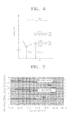
- FIG. 6 illustrates an energy level of Xe that is a source for generating ultraviolet rays.
- energy of 12.13eV is required to ionize Xe
- 8.28eV or more energy is required to excite Xe.
- energies 8.28eV, 8.45eV, and 9.57eV are required.
- the excited Xe (Xe + ) generates ultraviolet rays of 147nm wavelength while stabilizing.
- excimer Xe (Xe 2+ ) is generated.
- ultraviolet rays having about 173nm wavelength are generated.
- the electron beam that is emitted into the cell 314 by the electron emission source 340 can have an energy level of from about 8.28eV to about 12.13eV in order to excite Xe. Then, the electron beam may have the energy level from about 8.28eV to about 9.57eV or from about 8.28eV to about 8.45eV. Otherwise, the electron beam may have the energy level from about 8.45eV to about 9.57eV.
- FIG. 7 is a graph illustrating changes of relative dielectric constants of plastic materials according to frequencies of the materials.
- the first substrate or the second substrate is formed as a plastic substrate, the reason why the first or second substrate can be formed as a plastic substrate having a certain property will be described as follows.
- the dielectric constant of the plastic is generally lower than that of the glass, therefore a dielectric capacitance of the substrate can be reduced, and thus, invalid power consumption during driving the panel is reduced and luminous efficiency is improved.
- the above effects can be obtained by generating the electrons for exciting the gas using the electron emission source without generating a discharge or by generating a discharge with low voltage to reduce the heat transmitted to the first and second substrates.
- a relative dielectric constant of the glass epoxy is from about 4.1 to about 5.4
- a relative dielectric constant of a polyimide is from about 3.2 to about 3.8
- a relative dielectric constant of PTFE is from about 2 to about 2.2.
- the dielectric capacitance of the substrate that is formed of the above materials is just from about 2/3 to about 1/4 of the dielectric capacitance of the conventional glass substrate (a relative dielectric constant of PD200, which is an example of the glass for forming plasma display panel, is about 7.9). Therefore, the energy loss, that is, invalid power consumption, which is in proportion to the dielectric capacitance, can be reduced.
- the transmittance of the substrate with respect to the visible light is an important factor for selecting the material of the substrate.
- Table 2 illustrates examples of plastic materials that have relatively high transmittance for the visible light and can be used to form the front substrate.
- the plastic materials shown in above Table 2 have low relative dielectric constants, that is, from about 3 to about 4.5, the electric capacitance of the substrate that is formed of the above materials is from about 2/3 to about 1/4 of that of the conventional glass substrate, and the invalid power consumption can be reduced.
- the density of the plastic material is about half of the glass forming the plasma display panel or lower, and thus, the weight of the panel can be reduced.
- the weight of the substrate occupying a large amount of the panel weight and costs for fabricating the substrate can be reduced.
- the dielectric capacitance of the substrate can be reduced, and thus, the invalid power consumption when driving the panel can be reduced.
- the light transmittance of the panel is good, and thus, the luminous efficiency of the panel can be improved.
- the electron emission source is formed at an appropriate position, the electrons having the energy required to excite the gas can be generated without causing a discharge, or can be generated by causing the discharge at a low voltage to reduce the heat transmitted to the upper and lower substrates.
Landscapes
- Physics & Mathematics (AREA)
- Engineering & Computer Science (AREA)
- Plasma & Fusion (AREA)
- Gas-Filled Discharge Tubes (AREA)
- Led Devices (AREA)
- Vessels And Coating Films For Discharge Lamps (AREA)
- Illuminated Signs And Luminous Advertising (AREA)
Applications Claiming Priority (1)
| Application Number | Priority Date | Filing Date | Title |
|---|---|---|---|
| KR1020050111980A KR100787435B1 (ko) | 2005-11-22 | 2005-11-22 | 기체 여기 발광 소자 및 평판 표시장치 |
Publications (2)
| Publication Number | Publication Date |
|---|---|
| EP1788607A2 true EP1788607A2 (de) | 2007-05-23 |
| EP1788607A3 EP1788607A3 (de) | 2008-07-30 |
Family
ID=37831462
Family Applications (1)
| Application Number | Title | Priority Date | Filing Date |
|---|---|---|---|
| EP06124515A Withdrawn EP1788607A3 (de) | 2005-11-22 | 2006-11-21 | Vorrichtung zur Lichtemittierung durch Gaserregung |
Country Status (3)
| Country | Link |
|---|---|
| US (1) | US20070210710A1 (de) |
| EP (1) | EP1788607A3 (de) |
| KR (1) | KR100787435B1 (de) |
Cited By (2)
| Publication number | Priority date | Publication date | Assignee | Title |
|---|---|---|---|---|
| EP2219202A1 (de) * | 2009-02-17 | 2010-08-18 | Samsung SDI Co., Ltd. | Plasmaanzeigetafel und Verfahren zu deren Herstellung |
| US8217575B2 (en) | 2009-10-12 | 2012-07-10 | Samsung Sdi Co., Ltd. | Plasma display panel |
Families Citing this family (2)
| Publication number | Priority date | Publication date | Assignee | Title |
|---|---|---|---|---|
| JP2009252347A (ja) * | 2008-04-01 | 2009-10-29 | Panasonic Corp | プラズマディスプレイパネルおよびその製造方法 |
| JP5129674B2 (ja) * | 2008-07-09 | 2013-01-30 | パナソニック株式会社 | 発光装置 |
Citations (5)
| Publication number | Priority date | Publication date | Assignee | Title |
|---|---|---|---|---|
| GB2297862A (en) | 1995-02-08 | 1996-08-14 | Smiths Industries Plc | Displays |
| EP0886295A2 (de) | 1997-06-19 | 1998-12-23 | Sumitomo Chemical Company, Limited | Frontscheibe für Plasma-Anzeige |
| JP2002150944A (ja) | 2000-11-14 | 2002-05-24 | Matsushita Electric Works Ltd | 電子エミッタ付発光装置 |
| WO2004086449A1 (en) | 2003-03-26 | 2004-10-07 | Kim, Yong Seog | Front panel for plasma display panel of high efficiency containing nanotips, and process for preparation of the same |
| US20040263055A1 (en) | 2003-06-30 | 2004-12-30 | Chin-Hsiao Chao | Electrode substrate of flat panel display |
Family Cites Families (6)
| Publication number | Priority date | Publication date | Assignee | Title |
|---|---|---|---|---|
| TW391022B (en) * | 1997-10-29 | 2000-05-21 | Mitsubishi Rayon Co | Field emission electron source, method of producing the same, and use of the same |
| KR100438831B1 (ko) * | 2001-11-22 | 2004-07-05 | 삼성전자주식회사 | 플라즈마 평판 램프 |
| KR20050104551A (ko) * | 2004-04-29 | 2005-11-03 | 삼성에스디아이 주식회사 | 전자 방출 소자와, 이를 이용한 평면 표시 장치 |
| US20060132050A1 (en) * | 2004-12-18 | 2006-06-22 | Samsung Sdi Co., Ltd. | Display device |
| US20070080896A1 (en) * | 2005-10-07 | 2007-04-12 | Seung-Hyun Son | Display device |
| KR100751348B1 (ko) * | 2005-11-03 | 2007-08-22 | 삼성에스디아이 주식회사 | 표시 장치 |
-
2005
- 2005-11-22 KR KR1020050111980A patent/KR100787435B1/ko not_active Expired - Fee Related
-
2006
- 2006-11-16 US US11/600,692 patent/US20070210710A1/en not_active Abandoned
- 2006-11-21 EP EP06124515A patent/EP1788607A3/de not_active Withdrawn
Patent Citations (5)
| Publication number | Priority date | Publication date | Assignee | Title |
|---|---|---|---|---|
| GB2297862A (en) | 1995-02-08 | 1996-08-14 | Smiths Industries Plc | Displays |
| EP0886295A2 (de) | 1997-06-19 | 1998-12-23 | Sumitomo Chemical Company, Limited | Frontscheibe für Plasma-Anzeige |
| JP2002150944A (ja) | 2000-11-14 | 2002-05-24 | Matsushita Electric Works Ltd | 電子エミッタ付発光装置 |
| WO2004086449A1 (en) | 2003-03-26 | 2004-10-07 | Kim, Yong Seog | Front panel for plasma display panel of high efficiency containing nanotips, and process for preparation of the same |
| US20040263055A1 (en) | 2003-06-30 | 2004-12-30 | Chin-Hsiao Chao | Electrode substrate of flat panel display |
Cited By (3)
| Publication number | Priority date | Publication date | Assignee | Title |
|---|---|---|---|---|
| EP2219202A1 (de) * | 2009-02-17 | 2010-08-18 | Samsung SDI Co., Ltd. | Plasmaanzeigetafel und Verfahren zu deren Herstellung |
| US8237362B2 (en) | 2009-02-17 | 2012-08-07 | Samsung Sdi Co., Ltd. | Plasma display panel and method of manufacturing the same |
| US8217575B2 (en) | 2009-10-12 | 2012-07-10 | Samsung Sdi Co., Ltd. | Plasma display panel |
Also Published As
| Publication number | Publication date |
|---|---|
| US20070210710A1 (en) | 2007-09-13 |
| KR20070054026A (ko) | 2007-05-28 |
| EP1788607A3 (de) | 2008-07-30 |
| KR100787435B1 (ko) | 2007-12-26 |
Similar Documents
| Publication | Publication Date | Title |
|---|---|---|
| US20060132050A1 (en) | Display device | |
| EP1788607A2 (de) | Vorrichtung zur Lichtemittierung durch Gaserregung | |
| JP3178816B2 (ja) | ガス放電表示装置 | |
| KR100696541B1 (ko) | 전자방출수단을 구비한 플라즈마 디스플레이 패널 | |
| US20070046571A1 (en) | Plasma display panel | |
| KR100719574B1 (ko) | 평판 디스플레이 장치 및 전자 방출 소자 | |
| US20070132390A1 (en) | Display device | |
| KR100696506B1 (ko) | 평판 디스플레이 장치 | |
| US7486023B2 (en) | Single layer discharge electrode configuration for a plasma display panel | |
| KR100542223B1 (ko) | 플라즈마 디스플레이 패널 | |
| EP1783801A2 (de) | Anzeigetafel | |
| KR100741083B1 (ko) | 디스플레이 장치 | |
| KR100751344B1 (ko) | 표시 장치 | |
| KR100768189B1 (ko) | 표시 장치 | |
| US7518312B2 (en) | Plasma display panel (PDP) having low capacitance and high discharge efficiency | |
| KR100719584B1 (ko) | 표시장치 | |
| US20080265784A1 (en) | Gas excitation light-emitting device | |
| EP1772887A1 (de) | Anzeigevorrichtung | |
| KR20050112307A (ko) | 플라즈마 디스플레이 패널 | |
| KR100659104B1 (ko) | 디스플레이 장치 | |
| US20070152589A1 (en) | Plasma display panel | |
| US20070132394A1 (en) | Display device | |
| US20070063642A1 (en) | Plasma display panel | |
| JP2006073515A (ja) | 改善された電極構造を有するプラズマディスプレイパネル | |
| US20070080371A1 (en) | Display device |
Legal Events
| Date | Code | Title | Description |
|---|---|---|---|
| PUAI | Public reference made under article 153(3) epc to a published international application that has entered the european phase |
Free format text: ORIGINAL CODE: 0009012 |
|
| 17P | Request for examination filed |
Effective date: 20061121 |
|
| AK | Designated contracting states |
Kind code of ref document: A2 Designated state(s): AT BE BG CH CY CZ DE DK EE ES FI FR GB GR HU IE IS IT LI LT LU LV MC NL PL PT RO SE SI SK TR |
|
| AX | Request for extension of the european patent |
Extension state: AL BA HR MK YU |
|
| PUAL | Search report despatched |
Free format text: ORIGINAL CODE: 0009013 |
|
| RIC1 | Information provided on ipc code assigned before grant |
Ipc: H01J 61/30 20060101ALI20080616BHEP Ipc: H01J 5/04 20060101ALI20080616BHEP Ipc: H01J 17/04 20060101ALI20080616BHEP Ipc: H01J 17/16 20060101ALI20080616BHEP Ipc: H01J 17/49 20060101AFI20070315BHEP |
|
| AK | Designated contracting states |
Kind code of ref document: A3 Designated state(s): AT BE BG CH CY CZ DE DK EE ES FI FR GB GR HU IE IS IT LI LT LU LV MC NL PL PT RO SE SI SK TR |
|
| AX | Request for extension of the european patent |
Extension state: AL BA HR MK RS |
|
| 17Q | First examination report despatched |
Effective date: 20081127 |
|
| AKX | Designation fees paid |
Designated state(s): DE FR GB |
|
| RAP1 | Party data changed (applicant data changed or rights of an application transferred) |
Owner name: SAMSUNG SDI CO., LTD. |
|
| STAA | Information on the status of an ep patent application or granted ep patent |
Free format text: STATUS: THE APPLICATION IS DEEMED TO BE WITHDRAWN |
|
| 18D | Application deemed to be withdrawn |
Effective date: 20100601 |