EP1793304A2 - Appareil de traitement d'informations et procédé de fabrication correspondant - Google Patents
Appareil de traitement d'informations et procédé de fabrication correspondant Download PDFInfo
- Publication number
- EP1793304A2 EP1793304A2 EP06077019A EP06077019A EP1793304A2 EP 1793304 A2 EP1793304 A2 EP 1793304A2 EP 06077019 A EP06077019 A EP 06077019A EP 06077019 A EP06077019 A EP 06077019A EP 1793304 A2 EP1793304 A2 EP 1793304A2
- Authority
- EP
- European Patent Office
- Prior art keywords
- display panel
- front cover
- cover
- substrate
- rear cover
- Prior art date
- Legal status (The legal status is an assumption and is not a legal conclusion. Google has not performed a legal analysis and makes no representation as to the accuracy of the status listed.)
- Withdrawn
Links
Images






Classifications
-
- G—PHYSICS
- G06—COMPUTING OR CALCULATING; COUNTING
- G06F—ELECTRIC DIGITAL DATA PROCESSING
- G06F1/00—Details not covered by groups G06F3/00 - G06F13/00 and G06F21/00
- G06F1/16—Constructional details or arrangements
- G06F1/1613—Constructional details or arrangements for portable computers
-
- G—PHYSICS
- G06—COMPUTING OR CALCULATING; COUNTING
- G06F—ELECTRIC DIGITAL DATA PROCESSING
- G06F1/00—Details not covered by groups G06F3/00 - G06F13/00 and G06F21/00
- G06F1/16—Constructional details or arrangements
- G06F1/1613—Constructional details or arrangements for portable computers
- G06F1/1633—Constructional details or arrangements of portable computers not specific to the type of enclosures covered by groups G06F1/1615 - G06F1/1626
- G06F1/1637—Details related to the display arrangement, including those related to the mounting of the display in the housing
-
- G—PHYSICS
- G02—OPTICS
- G02F—OPTICAL DEVICES OR ARRANGEMENTS FOR THE CONTROL OF LIGHT BY MODIFICATION OF THE OPTICAL PROPERTIES OF THE MEDIA OF THE ELEMENTS INVOLVED THEREIN; NON-LINEAR OPTICS; FREQUENCY-CHANGING OF LIGHT; OPTICAL LOGIC ELEMENTS; OPTICAL ANALOGUE/DIGITAL CONVERTERS
- G02F1/00—Devices or arrangements for the control of the intensity, colour, phase, polarisation or direction of light arriving from an independent light source, e.g. switching, gating or modulating; Non-linear optics
- G02F1/01—Devices or arrangements for the control of the intensity, colour, phase, polarisation or direction of light arriving from an independent light source, e.g. switching, gating or modulating; Non-linear optics for the control of the intensity, phase, polarisation or colour
- G02F1/13—Devices or arrangements for the control of the intensity, colour, phase, polarisation or direction of light arriving from an independent light source, e.g. switching, gating or modulating; Non-linear optics for the control of the intensity, phase, polarisation or colour based on liquid crystals, e.g. single liquid crystal display cells
- G02F1/133—Constructional arrangements; Operation of liquid crystal cells; Circuit arrangements
- G02F1/1333—Constructional arrangements; Manufacturing methods
- G02F1/133308—Support structures for LCD panels, e.g. frames or bezels
-
- G—PHYSICS
- G06—COMPUTING OR CALCULATING; COUNTING
- G06F—ELECTRIC DIGITAL DATA PROCESSING
- G06F1/00—Details not covered by groups G06F3/00 - G06F13/00 and G06F21/00
- G06F1/16—Constructional details or arrangements
- G06F1/1613—Constructional details or arrangements for portable computers
- G06F1/1626—Constructional details or arrangements for portable computers with a single-body enclosure integrating a flat display, e.g. Personal Digital Assistants [PDAs]
-
- G—PHYSICS
- G02—OPTICS
- G02F—OPTICAL DEVICES OR ARRANGEMENTS FOR THE CONTROL OF LIGHT BY MODIFICATION OF THE OPTICAL PROPERTIES OF THE MEDIA OF THE ELEMENTS INVOLVED THEREIN; NON-LINEAR OPTICS; FREQUENCY-CHANGING OF LIGHT; OPTICAL LOGIC ELEMENTS; OPTICAL ANALOGUE/DIGITAL CONVERTERS
- G02F2201/00—Constructional arrangements not provided for in groups G02F1/00 - G02F7/00
- G02F2201/46—Fixing elements
Definitions
- the present general inventive concept relates to an information processing apparatus and a manufacturing method thereof, and more particularly, to an information processing apparatus which is assembled without difficulty and has a light and simple configuration, and a manufacturing method thereof.
- an information processing apparatus processes various information to provide convenience to a user.
- the information processing apparatus comprises an MP3 player, a personal digital assistant (PDA), a cell phone, a digital camera, a digital photo frame and a portable multimedia player (PMP).
- the information processing apparatus may further comprise a portable computer.
- the information processing apparatus comprises a mounting slot to detachably attach a peripheral device, such as a secure digital (SD) card, a compact flash (CF) card, a multi media card (MMC) and a universal serial bus (USB), thereto, to input information or data as necessary.
- a peripheral device such as a secure digital (SD) card, a compact flash (CF) card, a multi media card (MMC) and a universal serial bus (USB), thereto, to input information or data as necessary.
- SD secure digital
- CF compact flash
- MMC multi media card
- USB universal serial bus
- the conventional information processing apparatus comprises a front cover which has an opening, a display panel having a display part exposed to an outside through the opening of the front cover; and a circuit such as a printed circuit board (PCB) which is provided on a rear part of the display panel to drive the display panel.
- the conventional information processing apparatus further comprises a shield cover which protects the PCB from an external force and blocks an electromagnetic wave generated by the PCB, and a rear cover which is coupled with the front cover, to accommodate the display panel, the circuit or the shield cover therebetween.
- the display panel, the circuit or the shield cover is coupled with the front cover by a screw, and then the rear cover is coupled with the front cover by a screw.
- the display panel or the circuit is coupled with the front cover by a screw, thereby causing a complex configuration and assembly process. Also, since a part of the information processing apparatus that is coupled by a screw is relatively thick, the information processing apparatus becomes heavy in weight and components thereof are enlarged in size.
- the present general inventive concept provides an information processing apparatus which is assembled without difficulty and stably supported and has a light and simple configuration, and a manufacturing method thereof.
- an information processing apparatus which comprises a front cover having a display opening to display an image of a display panel and a rear cover which is coupled with the front cover, the apparatus further comprising at least one holder which is formed on a first end of the front cover to prevent the display panel from being separated from the front cover, and a movable holder which is provided on a second end of the front cover to face the holder and prevents the display panel from being separated from the front cover.
- the information processing apparatus may further comprise a main circuit substrate which is mounted on a rear part of the display panel to drive the display panel, and a shield cover which is disposed between the main circuit substrate and the rear cover to protect the main circuit substrate.
- the rear cover may comprise a plurality of pressure projections which is formed on an internal plate surface of the rear cover to press the display panel, the main circuit substrate, and the shield cover toward the front cover.
- the front cover may comprise a pin which is formed on an internal plate surface thereof, and wherein the movable holder comprises a pin accommodator which is coupled with the pin to maintain a position of the front cover.
- the movable holder may comprise a substrate coupling part which is formed on a plate surface thereof in a transverse direction to a plate surface of the display panel to support an auxiliary circuit substrate.
- the rear cover may comprise a plurality of rear cover coupling holes, and wherein the front cover comprises a front cover coupling part which is coupled with the rear cover coupling holes, and wherein the main circuit substrate and the shield cover comprise a main substrate hole and a shield cover hole which are formed on a predetermined position corresponding to the rear cover coupling holes and the front cover coupling part, respectively.
- an information processing apparatus which has a front cover having a display opening to display an image of a display panel and a rear cover which is coupled with the front cover, the method comprising forming at least one holder on a first end of the front cover to prevent the display panel from being separated from the front cover, and providing a movable holder on a second end of the front cover to face the holder and preventing the display panel from being separated from the front cover.
- the method may further comprise mounting a main circuit substrate on a rear part of the display panel to drive the display panel; and disposing a shield cover between the main circuit substrate and the rear cover to protect the main circuit substrate.
- the method may further comprise forming a plurality of pressure projections on an internal plate surface of the rear cover to press the display panel, the main circuit substrate, and the shield cover toward the front cover.
- an information processing apparatus which comprises a front cover having a display opening to display an image of a display panel and a rear cover which is coupled with the front cover, the information processing apparatus comprising a main substrate which is provided behind the display panel, and an auxiliary substrate which is disposed in a transverse direction of a plate surface of the main substrate and mounted between the front and rear covers to drive the display panel.
- the main substrate may comprise at least one ground pin which is formed on the plate surface of the main substrate and elastically presses the display panel.
- the information processing apparatus may further comprise an auxiliary substrate bracket which is provided between the front cover and the rear cover and supports the auxiliary substrate.
- the front cover may be formed with at least one coupling pin which is formed on an internal plate surface thereof, and the auxiliary substrate bracket is formed with a coupling pin accommodator which is coupled with the coupling pin.
- the information processing apparatus may further comprise a substrate shield cover which is provided between the main substrate and the rear cover to protect the main substrate.
- the plate surface of the main substrate may be provided in parallel with the plate surface of the display panel.
- the rear cover may comprise at least one supporting projection which includes a bracket slot formed on the internal plate surface thereof and accommodating the auxiliary substrate bracket.
- an information processing apparatus which has a front cover having a display opening to display an image of a display panel and a rear cover which is coupled with the front cover, the method comprising providing a main substrate behind the display panel that is coupled with the front cover, and mounting an auxiliary substrate in a transverse direction of a plate surface of the main substrate between the front cover and the rear cover to be spaced from the display panel and the main substrate.
- the method may further comprise supporting the auxiliary substrate by an auxiliary substrate bracket which is disposed between the front cover and the rear cover.
- the method may further comprise forming at least one coupling pin in an internal surface of the front cover, and forming a coupling pin accommodator which is coupled with the coupling pin, in the auxiliary substrate bracket.
- the method may further comprise providing a substrate shield cover between the main substrate and the rear cover to protect the main substrate.
- the method may further comprise forming at least one supporting projection which includes a bracket slot to accommodate the auxiliary substrate bracket, in the rear cover.
- an information processing apparatus having a front cover, a rear cover coupled to the front cover, and a display panel disposed between the front cover and the rear cover, the information processing apparatus including a holder formed on a first portion of the front cover to hold a first end of a display panel, a movable holder disposed on a second portion of the front cover to hold a second end of the display panel, a main substrate disposed between the rear cover and a first portion of the display panel to drive the display panel, and an auxiliary substrate disposed between the rear cover and a second portion of the display panel to drive the display panel.
- an information processing apparatus having a front cover, a rear cover coupled to the front cover, and a display panel disposed between the front cover and the rear cover, the method including forming a holder on a first portion of the front cover to hole a first end of a display panel, disposing a movable holder on a second portion of the front cover to hold a second end of the display panel, disposing a main substrate between the rear cover and a first portion of the display panel to drive the display panel, and disposing an auxiliary substrate between the rear cover and a second portion of the display panel to drive the display panel.
- FIG.1 is a perspective view illustrating an information processing apparatus 10 to process various information.
- the information processing apparatus 10 comprises an MP3 player, a digital photo frame, a personal digital assistant (PDA), a cell phone, and a portable multimedia player (PMP).
- the information processing apparatus 10 may further comprise a display apparatus such as a monitor of a personal computer which displays a signal input from an external signal source, or may be a portable computer.
- the digital photo frame will be described as an example of the information processing apparatus 10 according to the present embodiment.
- the digital photo frame is installed on an installing surface such as a table or a wall and comprises a display panel which displays an image thereon.
- the digital photo frame displays the image which is supplied by a memory card inserted into a slot thereof, instead of inputting an image, a moving picture or an MP3 file captured by a digital camera, etc. to a computer. That is, a user may play or view a moving picture or an image recorded by a digital camera or a camcorder by directly using the digital photo frame.
- the digital photo frame produces the desired effect as an interior accessory like a photo frame, while displaying the image.
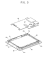
- the information processing apparatus 10 comprises a front cover 20 having a display opening 21 to display an image formed on a screen of a display panel 50, a rear cover 30 which is coupled with the front cover 20, one or more holders 61a and 61b which are formed on a first end of an inside surface of the front cover 20 in a transverse direction to prevent the display panel 50 from being separated from the front cover 20, and a movable holder 70 which is provided on a second end of the inside surface of the front cover 20 to face the holders 61a and 61b and prevents the display panel 50 from being separated from the front cover 20.
- the information processing apparatus 10 further comprises a main circuit substrate 85 which is mounted on a rear part of the display panel 50 to drive the display panel 50, and a shield cover 90 which is disposed between the main circuit substrate 85 and the rear cover 30 to protect the main circuit substrate 85.
- the information processing apparatus 10 further comprises a supporting bracket 13 which is installed on an installing surface, such as a table, to support the information processing apparatus 10 with respect to the installing surface.
- the front cover 20 comprises the display opening 21 through which a display part of the display panel 50 is exposed to an outside.
- the display opening 21 of the front cover 20 has a rectangular shape, but not limited thereto. Alternatively, the display opening 21 of the front cover 20 may have various shapes.
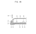
- the front cover 20 further comprises a panel mounting part 60 to which the display panel 50 is mounted, pins 23a and 23b which are formed on a plate surface(the inside surface) of the front cover 20 to be coupled with the movable holder 70, and a front cover coupling part 25 which is coupled with the rear cover 30 by a screw 36(FIG. 4A).
- the front cover 20 is coupled with the rear cover 30, thereby forming an external appearance of the information processing apparatus 10 together with the display panel 50.
- the pins 23a and 23b are formed on a rear surface(inside surface) of the front cover 20 to be coupled with pin accommodators 71a and 71b of the movable holder 70.
- the pins 23a and 23b are disposed adjacent to the panel mounting part 60 provided on a rear upper part of the front cover 20, facing the holders 61a and 61b with respect to the display opening 21.
- the rear cover 30 is coupled with the front cover 20 and comprises rear cover coupling holes 31 which are coupled with coupling pins 22 of the front cover 20to accommodate the display panel 50, the main circuit substrate 85, an auxiliary circuit substrate 80, the movable holder 70, and the shield cover 90 therebetween.
- the rear cover 30 further comprises a mounting slot 45 which detachably attaches a peripheral device (not shown) thereto, and a door 40 which rotatably opens and closes the mounting slot 45.
- a pressure projection 33 is formed on an internal plate surface of the rear cover 30 to press the display panel 50, the main circuit substrate 85, and the shield cover 90 toward the front cover 20 as illustrated in FIG. 4A.
- the pressure projection 33 may comprise a groove 35 into which a substrate coupling part 73 of the movable holder 70 disposed in a coupling direction of the front cover 20 and the rear cover 30 is inserted to support the movable holder 70. Accordingly, an additional coupling unit such as a screw is unnecessary to couple components provided between the front and rear covers 20 and 30 as illustrated in FIGS. 4A and 4B.
- the display panel 50 is stably supported by the pressure projection 33.
- the information processing apparatus 10 may comprise a light and simple configuration.
- the front cover 20 and the rear cover 30 may comprise a flame retardant material such as polycarbonate and acrylonitrile butadiene styrene.
- the door 40 is coupled with the rear cover 30 by a hinge to rotatably open and close the mounting slot 45.
- a shape of the door 40 may correspond to that of the mounting slot 45 to cover the mounting slot 45.
- the display panel 50 is coupled with the front cover 20 such that a screen is exposed through display opening 21 of the front cover 20 to display an image thereon through wired and wireless signals generated from the main circuit substrate 85 or an external device connected to the main circuit substrate 85.
- the display panel 50 may comprise a liquid crystal display (LCD) which displays an image on a thin plate having pixels by supplying an electrode, a plasma display panel (PDP) which applies gas discharging principles or other conventional panels.
- LCD liquid crystal display
- PDP plasma display panel
- the panel mounting part 60 is formed along a circumferential part of the front cover 20 to mount the display panel 50 thereon.
- the panel mounting part 60 is supported by the holders 61a and 61b.
- the holders 61a and 61b are formed on the first end of the front cover 20 to prevent the display panel 50 from being separated from the front cover 20.
- the holders 61a and 61b are projected and bent from the first end of the front cover 20 and have a C-shape. There are provided one or more holders 61a and 61b.
- the movable holder 70 is provided on the second end of the front cover 20 to face the holders 61a and 61b with respect to the display opening 21 and prevents the display panel 50 from being separated from the front cover 20.
- the movable holder 70 is disposed on a rear upper part of the front cover 20to hold or bias the display panel 50 toward the holders 61a and 61b.
- the display panel 50 is supported by the holders 61a and 61b provided on the rear lower part of the front cover 20 and by the movable holder 70 provided on the rear upper part of the front cover 20, without an additional coupling unit such as a screw.
- the information processing apparatus 10 may comprise a light and simple configuration.
- the movable holder 70 comprises the substrate coupling part 73 which supports an auxiliary circuit substrate 80 (to be described later).
- the auxiliary circuit substrate 80 is coupled and supported by the substrate coupling part 73 formed on a plate surface of the movable holder 70 in a transverse direction of a plate surface of the display panel 50.
- the plate surface of the display panel 50 may be perpendicular to the plate surface of the movable holder 70 and may be parallel to the screen to display the image.
- the auxiliary circuit substrate 80 is electrically coupled with the display panel 50 to provide various illumination to the display panel 50.
- the main circuit substrate 85 is disposed on a rear part of the display panel 50 and electrically coupled therewith to display an image on the screen of the display panel 50, and provides/records predetermined information.
- the main circuit substrate 85 comprises a plurality of main substrate holes 87 formed on a predetermined position corresponding to the front cover coupling part 25 and the rear cover coupling holes 31.
- the main circuit substrate 85 is coupled with the front cover 20 and the rear cover 30 without an additional coupling unit, such as a screw, and comprises a simple configuration.
- the shield cover 90 is provided on a rear part of the main circuit substrate 85 to protect the main circuit substrate 85.
- the shield cover 90 comprises a metal material to block an electromagnetic wave generated by the main circuit substrate 85.
- the shield cover 90 comprises a plurality of shield cover holes 91 which are provided on a predetermined position corresponding to the front cover coupling part 25 and the rear cover coupling holes 31.
- the shield cover 90 is coupled with the front cover 20 and the rear cover 30 without an additional coupling unit such as a screw, and comprises a simple supporting configuration.
- the front cover coupling part 25 may be a boss to be inserted into the main substrate hole 87, the shield cover holes 91, and the rear cover coupling hole 31, so that the front cover 20 is coupled to the rear cover 30 without a screw.
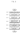
- the front cover 20 is disposed on a worktable (not shown). Here, a front surface of the front cover 20 faces the worktable.
- the display panel 50 is inserted into the front cover 20 and mounted to the holders 61a and 61b (S105).
- the pin accommodators 71a and 71b of the movable holder 70 are coupled with the pins 23a and 23b so that the movable holder 70 is disposed on a predetermined position to press the display panel 50 (S110).
- the main circuit substrate 85 is stably seated on the display panel 50 (S115).
- the shield cover 90 is disposed on an upper part of the main circuit substrate 85 to couple the shield cover holes 91 of the shield cover 90 with the front cover coupling part 25 (S120).
- the plurality of pressure projections 33 is formed on an inside plate surface of the rear cover 30 to press the display panel 50, the main circuit substrate 85, and the shield cover 90 toward the front cover 20 (S125).
- the rear cover 30 is disposed on the shield cover 90 so that the front cover coupling part 25 corresponds to the rear cover coupling holes 31, and coupled with the front cover 20 by a screw 36 (S130). Then, the pressure projections 33 of the rear cover 30 press the display panel 50, the movable holder 70, the main circuit substrate 85, and the shield cover 90 toward the front cover 20.
- the front coupling part 25 is formed as the boss to be coupled to the rear cover 30 as described above, the screw 36 may be used to couple the boss and the rear cover 30.
- the digital photo frame is provided as an example of the present general inventive concept, but not limited thereto.
- the present invention can be applicable to a portable information processing apparatus such as a PDA and a PMP.
- the information processing apparatus is assembled without difficulty, is stably supported, and comprises a light and simple configuration.
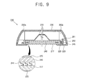
- an information processing apparatus 210 comprises a front cover 220 having a display opening 221 through which an image formed on a screen of a display panel 217is displayed a rear cover 230 which is coupled with the front cover 220, a main substrate 240 which is provided behind the display panel 217 to drive the display panel 217, and an auxiliary substrate 245 which is mounted between the front cover 220 and the rear cover 230 to be provided in a transverse direction of the main substrate 240 and spaced from the display panel 217 and the main substrate 240.
- the information processing apparatus 210 further comprises a substrate shield cover 270 which is provided between the main substrate 240 and the rear cover 230 to protect the main substrate 240.
- the information processing apparatus 210 further comprises a supporting bracket 213 which is installed on an installing surface such as a desk to support the rear cover 230 with respect to the installing surface.
- a door 215 is coupled with the rear cover 230 by a hinge and rotatably opens and closes a mounting slot 216.
- a shape of the door 215 may correspond to that of the mounting slot 216 of the rear cover 230 to cover the mounting slot 216.
- the front cover 220 comprises the display opening 221 through which a display part of the display panel 217 is exposed.
- the display opening 221 of the front cover 220 has a rectangular shape but not limited thereto. Alternatively, a shape of the display opening 221 may vary.
- the front cover 220 comprises a coupling pin 223(223a and 223b) which is formed on an inside plate surface of the front cover 220 and coupled with an auxiliary substrate bracket 250, and a panel mounting part 225 in which the display panel 217 is mounted.
- the front cover 220 is coupled with the rear cover 230, thereby completing an external appearance of the information processing apparatus 210 together with the display panel 217.
- the coupling pins 223a and 223b are formed on the inside plate surface of the front cover 220 and coupled with a coupling pin accommodator 251(251a and 251b) of the auxiliary substrate bracket 250.
- the panel mounting part 225 is formed on a circumference of the front cover 220 in which the display panel 217 is mounted.
- the rear cover 230 may be coupled with the front cover 220 by a screw, etc.
- the display panel 217, the main substrate 240, the auxiliary substrate 245, the auxiliary substrate bracket 250, and the substrate shield cover 270 are provided between the front cover 220 and the rear cover 230.
- the rear cover 230 is provided with a supporting projection 260 formed on an inside plate surface thereof.
- the supporting projection 260 comprises a bracket slot 261 to accommodate the auxiliary substrate bracket 250.
- the rear cover 230 is provided with the mounting slot 216 to which a peripheral device (not shown) is detachably mounted, and the door 215 which rotatably opens and closes the mounting slot 216.
- the front cover 220 and the rear cover 230 comprise resin such as polycarbonate and acrylonitrile butadiene styrene which are resistant to fire.
- the main substrate 240 and the auxiliary substrate 245 are electrically coupled with each other and provided behind the display panel 217.
- the main substrate 240 and the auxiliary substrate 245 are electrically coupled with the display panel 217 and drive the display panel 217 to display an image.
- the main substrate 240 may drive a flash memory, an SD card and a CF card, as well as the display panel 217 to generate and display the image.
- a plate surface of the main substrate 240 is provided in parallel with a plate surface of the display panel 217.
- the main substrate 240 and the auxiliary substrate 245 are not stacked and spaced from each other.
- the main substrate 240 is disposed on a first portion of the display panel 217 and the auxiliary substrate 245 is disposed on a second portion of the display panel 217.
- the information processing apparatus 210 becomes relatively slim.
- a plurality of integrated circuits (IC) (not illustrated) is mounted in opposite lateral parts of the main substrate 240.
- the main substrate 240 further comprises at least one ground pin 241 which is formed on the plate surface thereof and elastically presses the display panel 217.
- At least one ground pin 241 is formed on the plate surface of the main substrate 240 and projected toward the display panel 217 to elastically press the display panel 217.
- the ground pin 241 comprises copper which is elastic.
- the ground pin 241 may be variously disposed on the plate surface of the main substrate 240 as necessary.
- the ground pin 241 makes the main substrate 240 connected with ground and also prevents the ICs of the main substrate 240 from being in contact with the display panel 217.
- the ground pin 241 may be in plural and may have a first portion extended from the main substrate 240 and a second portion extended from the first portion toward the display panel 217. A distal end of the second portion is bent.
- the display panel 217 and the main substrate 240 maintain spaced-apart by the ground pin 241.
- the auxiliary substrate 245 is coupled with a substrate coupling part 253 which is formed on the auxiliary substrate bracket 250 in a transverse direction of the plate surface of the display panel 217.
- the auxiliary substrate 245 is electrically coupled with the display panel 217 to provide various levels of brightness to the display panel 217.
- the auxiliary substrate 245 is supported by a bracket slot 261 of the rear cover 230 and the front cover 220. As the main substrate 240 and the auxiliary substrate 245 are not stacked with each other, the information processing apparatus 210 remains slim.
- a power supply and a circuit driver of the main substrate 240 and the auxiliary substrate 245 are separated from each other, thereby supplying signals and power to the display panel 217 stably.
- the auxiliary substrate bracket 250 is coupled by the bracket slot 261 of the rear cover 230 to the front cover 220.
- the auxiliary substrate bracket 250 comprises the coupling pin accommodator 251(251a and 251b) which is formed on the plate surface thereof and coupled with the coupling pin 223.
- the auxiliary substrate bracket 250 further comprises the substrate coupling part 253 which is coupled with the auxiliary substrate 245. As the auxiliary substrate 245 and the main substrate 240 are not stacked with each other, the information processing apparatus 210 remains relatively slim.
- At least one supporting projection 260 is formed on an inside plate surface of the rear cover 230 to press the circumference of the display panel 217, the main substrate 240, and the substrate shield cover 270 toward the front cover 220.
- the supporting projection 260 comprises the bracket slot 261 which accommodates the auxiliary substrate bracket 250.
- an additional coupling unit such as a screw is not necessary.
- As the auxiliary substrate 245 is coupled with the auxiliary substrate bracket 250 on an area where it is separated from the main substrate 240, thereby maintaining the information processing apparatus 210 slim.
- the substrate shield cover 270 is provided behind the main substrate 240 and protects the main substrate 240.
- the substrate shield cover 270 comprises metal to block electronic waves which are generated by the main substrate 240.
- the front cover 220 is disposed on a working table (not shown) (S305).
- the display panel 217 is mounted in the front cover 220 (S310).
- the auxiliary substrate bracket 250 is mounted in the front cover 220 to support the auxiliary substrate 245 on an area where the display panel 217 is spaced therefrom, and couple the coupling pin 223 (223a and 223b) with the coupling pin accommodator 251 (251a and 251b) (S315).
- the auxiliary substrate 245 may be electrically connected with the display panel 217 through a connector or a cable(not illustrated).
- the main substrate 240 is disposed on the display panel 217 so that the plate surface of the main substrate 240 is provided in parallel with that of the display panel 217 (S320).
- the main substrate 240 formed with the ground pin 241 is disposed toward the display panel 217.
- the main substrate 240 may be electrically connected with the display panel 217 through another connector or another cable.
- the substrate shield cover 270 is provided on the main substrate 240 (S325).
- the circumference of the display panel 217, the main substrate 240, and the substrate shield cover 270 are coupled with the front cover 220 and the rear cover 230 to be pressed toward the front cover 220 (S330). That is, the supporting projection 260 of the rear cover 230 sequentially presses the display panel 217, the main substrate 240, and the substrate shield cover 270.
- the rear cover 230 is coupled with the front cover 220 so that the auxiliary substrate bracket 250 is coupled with the bracket slot 261 of the rear cover 230.
- the front cover 230 and the rear cover 230 of FIGS. 6-9 may be coupled in the similar manner to the front cover 20 and the rear cover 30 of FIGS. 1-5.
- the present general inventive concept can be applicable to a portable information processing apparatus such as a PDA and a PMP.
- the information processing apparatus becomes relatively slim as the components such as the auxiliary substrate mounted between the front and rear covers are not stacked with the each other and requires small space. Thus, the components can be stably supported.
- an information processing apparatus which is assembled without difficulty, stably supported and comprises a light and simple configuration, and a manufacturing method thereof are provided.
- the present invention provides an information processing apparatus which is relatively small and requires small space as components mounted between front and rear covers are not stacked with each other and supports components stably, and a manufacturing method thereof.
Landscapes
- Engineering & Computer Science (AREA)
- Physics & Mathematics (AREA)
- Theoretical Computer Science (AREA)
- Computer Hardware Design (AREA)
- General Physics & Mathematics (AREA)
- Nonlinear Science (AREA)
- General Engineering & Computer Science (AREA)
- Human Computer Interaction (AREA)
- Crystallography & Structural Chemistry (AREA)
- Optics & Photonics (AREA)
- Chemical & Material Sciences (AREA)
- Mathematical Physics (AREA)
- Devices For Indicating Variable Information By Combining Individual Elements (AREA)
Applications Claiming Priority (1)
| Application Number | Priority Date | Filing Date | Title |
|---|---|---|---|
| KR1020050116559A KR101164822B1 (ko) | 2005-12-01 | 2005-12-01 | 정보처리장치 및 그 제작방법 |
Publications (2)
| Publication Number | Publication Date |
|---|---|
| EP1793304A2 true EP1793304A2 (fr) | 2007-06-06 |
| EP1793304A3 EP1793304A3 (fr) | 2012-06-20 |
Family
ID=37769462
Family Applications (1)
| Application Number | Title | Priority Date | Filing Date |
|---|---|---|---|
| EP20060077019 Withdrawn EP1793304A3 (fr) | 2005-12-01 | 2006-11-15 | Appareil de traitement d'informations et procédé de fabrication correspondant |
Country Status (4)
| Country | Link |
|---|---|
| US (1) | US7952654B2 (fr) |
| EP (1) | EP1793304A3 (fr) |
| KR (1) | KR101164822B1 (fr) |
| CN (1) | CN100579343C (fr) |
Cited By (2)
| Publication number | Priority date | Publication date | Assignee | Title |
|---|---|---|---|---|
| EP2076108A3 (fr) * | 2007-12-28 | 2009-10-21 | ORION ELECTRIC CO., Ltd. | Dispositif d'affichage |
| WO2014145062A1 (fr) * | 2013-03-15 | 2014-09-18 | Honeywell International Inc. | Connecteur de décharge électrostatique et procédé pour un dispositif électronique |
Families Citing this family (9)
| Publication number | Priority date | Publication date | Assignee | Title |
|---|---|---|---|---|
| JP5039572B2 (ja) * | 2007-01-22 | 2012-10-03 | パナソニック株式会社 | 電子機器、撮像装置 |
| CN101449899A (zh) * | 2007-12-07 | 2009-06-10 | 鸿富锦精密工业(深圳)有限公司 | 数字相框 |
| JP2009162919A (ja) * | 2007-12-28 | 2009-07-23 | Orion Denki Kk | 表示装置 |
| JP5423051B2 (ja) * | 2009-02-27 | 2014-02-19 | 株式会社Jvcケンウッド | 表示モジュール、表示モジュールの固定構造、及び画像表示装置 |
| JP2011077446A (ja) * | 2009-10-01 | 2011-04-14 | Sanyo Electric Co Ltd | シールドケース及び画像表示装置 |
| CN102339561A (zh) * | 2010-07-22 | 2012-02-01 | 鸿富锦精密工业(深圳)有限公司 | 机壳及使用该机壳的显示设备 |
| JP2014089424A (ja) * | 2012-10-31 | 2014-05-15 | Toshiba Corp | 映像表示装置および電子機器 |
| US9690128B2 (en) * | 2014-07-25 | 2017-06-27 | Lg Display Co., Ltd. | Liquid crystal display apparatus |
| CN121548791A (zh) * | 2023-07-19 | 2026-02-17 | 三星电子株式会社 | 包括电池的连接构件的可折叠装置 |
Family Cites Families (21)
| Publication number | Priority date | Publication date | Assignee | Title |
|---|---|---|---|---|
| US5926660A (en) * | 1997-09-30 | 1999-07-20 | Eastman Kodak Company | Camera and mechanical timer mechanism |
| KR100252198B1 (ko) | 1997-10-06 | 2000-04-15 | 박호군 | 식물 병원성 곰팡이에 대한 길항작용을 가진 바실러스속 균주 |
| TW445386B (en) * | 1998-03-16 | 2001-07-11 | Hitachi Ltd | Thin-type display |
| KR100304190B1 (ko) | 1998-03-31 | 2001-10-19 | 윤종용 | 전자 디바이스를 위한 힌지가능하고 착탈가능한 액세스 도어 |
| KR200232049Y1 (ko) | 1998-12-02 | 2001-08-07 | 윤종용 | 액세스 도어를 갖는 휴대형 컴퓨터 |
| JP2000315054A (ja) * | 1999-04-30 | 2000-11-14 | Citizen Watch Co Ltd | 液晶表示装置 |
| KR200285944Y1 (ko) * | 1999-05-26 | 2002-08-22 | 삼성전자 주식회사 | 엘씨디 모니터의 샤시 고정장치 |
| JP3638232B2 (ja) * | 1999-08-27 | 2005-04-13 | ペンタックス株式会社 | カード挿脱機構 |
| JP4597301B2 (ja) * | 2000-02-16 | 2010-12-15 | エーユー オプトロニクス コーポレイション | 保持枠および液晶表示装置 |
| JP2001306000A (ja) * | 2000-04-21 | 2001-11-02 | Minolta Co Ltd | 積層型表示パネル及びその製造方法 |
| KR100793728B1 (ko) * | 2001-09-14 | 2008-01-10 | 삼성전자주식회사 | 액정 표시 장치 |
| JP2003167235A (ja) * | 2001-12-03 | 2003-06-13 | Nec Kagoshima Ltd | 液晶表示装置の組み立て構造及びその組み立て方法 |
| JP2003185994A (ja) * | 2001-12-14 | 2003-07-03 | Nanox Corp | 液晶表示装置 |
| KR100471064B1 (ko) * | 2002-06-11 | 2005-03-10 | 삼성전자주식회사 | 디스플레이장치 |
| KR100512718B1 (ko) | 2002-07-16 | 2005-09-07 | 삼성전자주식회사 | 모니터장치 |
| KR100889534B1 (ko) | 2002-07-24 | 2009-03-23 | 엘지디스플레이 주식회사 | Lcd 모듈의 액정패널 고정구조 |
| JP2004077955A (ja) * | 2002-08-21 | 2004-03-11 | Nec Kagoshima Ltd | 液晶表示装置 |
| KR200305308Y1 (ko) | 2002-10-14 | 2003-03-03 | 임형태 | 액정 모니터용 스탠드 |
| JP4155833B2 (ja) * | 2003-01-27 | 2008-09-24 | 株式会社エンプラス | 電気部品用ソケット |
| KR20040096097A (ko) | 2003-05-07 | 2004-11-16 | 여단열 | 스탠드형 액정표시장치 |
| TW200515036A (en) * | 2003-10-17 | 2005-05-01 | Au Optronics Corp | Grounding device of liquid crystal display circuit board |
-
2005
- 2005-12-01 KR KR1020050116559A patent/KR101164822B1/ko not_active Expired - Fee Related
-
2006
- 2006-11-15 EP EP20060077019 patent/EP1793304A3/fr not_active Withdrawn
- 2006-11-30 CN CN200610163143A patent/CN100579343C/zh not_active Expired - Fee Related
- 2006-11-30 US US11/606,238 patent/US7952654B2/en not_active Expired - Fee Related
Cited By (4)
| Publication number | Priority date | Publication date | Assignee | Title |
|---|---|---|---|---|
| EP2076108A3 (fr) * | 2007-12-28 | 2009-10-21 | ORION ELECTRIC CO., Ltd. | Dispositif d'affichage |
| US7791868B2 (en) | 2007-12-28 | 2010-09-07 | Orion Electric Co., Ltd. | Display device |
| WO2014145062A1 (fr) * | 2013-03-15 | 2014-09-18 | Honeywell International Inc. | Connecteur de décharge électrostatique et procédé pour un dispositif électronique |
| US9964326B2 (en) | 2013-03-15 | 2018-05-08 | Honeywell International Inc. | Electrostatic discharge connector and method for an electronic device |
Also Published As
| Publication number | Publication date |
|---|---|
| CN100579343C (zh) | 2010-01-06 |
| US7952654B2 (en) | 2011-05-31 |
| CN1976563A (zh) | 2007-06-06 |
| EP1793304A3 (fr) | 2012-06-20 |
| US20070126946A1 (en) | 2007-06-07 |
| KR101164822B1 (ko) | 2012-07-12 |
| KR20070058211A (ko) | 2007-06-08 |
Similar Documents
| Publication | Publication Date | Title |
|---|---|---|
| US6229695B1 (en) | Palm-sized computer with a frame to hold device plates | |
| US6842333B2 (en) | Portable electronic device having LCD and touch screen | |
| KR100322651B1 (ko) | 디스플레이 유니트 및 그 디스플레이 유니트를 사용한 노트북 컴퓨터 | |
| US20040004810A1 (en) | Computer system having interchangeable LCDs | |
| EP1416357A2 (fr) | Système d'ordinateur portable et sa méthode d'assemblage | |
| US7952654B2 (en) | Information processing apparatus and manufacturing method thereof | |
| EP3051335A1 (fr) | Appareil d'affichage | |
| US7268999B2 (en) | Display apparatus | |
| US7675743B2 (en) | Information processing apparatus | |
| US20080019086A1 (en) | Display apparatus having board assembly unit | |
| JP4694789B2 (ja) | パネル部材ユニットおよび電子機器並びに取り付け部材 | |
| KR20050099621A (ko) | 평판형 화상 표시 장치 | |
| CN101336402A (zh) | 电子设备 | |
| CN111480189B (zh) | 显示设备 | |
| CN101663632A (zh) | 电子设备 | |
| US20060210866A1 (en) | Electronic apparatus | |
| US20020149915A1 (en) | Computing device with a card receptacle | |
| US7447004B2 (en) | Portable display apparatus | |
| KR101249837B1 (ko) | 정보처리장치 및 그 제작방법 | |
| US7417874B2 (en) | Information processing apparatus having detachable front and rear covers | |
| WO2011067844A1 (fr) | Dispositif électronique | |
| EP2034744A1 (fr) | Appareil d'affichage et appareil à affichage multiple doté de celui-ci | |
| JP2004127596A (ja) | 電子機器およびその組立方法 | |
| US7333162B2 (en) | Display unit structure | |
| KR20010112538A (ko) | 액정표시장치 및 이를 채용한 정보처리장치 |
Legal Events
| Date | Code | Title | Description |
|---|---|---|---|
| PUAI | Public reference made under article 153(3) epc to a published international application that has entered the european phase |
Free format text: ORIGINAL CODE: 0009012 |
|
| AK | Designated contracting states |
Kind code of ref document: A2 Designated state(s): AT BE BG CH CY CZ DE DK EE ES FI FR GB GR HU IE IS IT LI LT LU LV MC NL PL PT RO SE SI SK TR |
|
| AX | Request for extension of the european patent |
Extension state: AL BA HR MK YU |
|
| RIC1 | Information provided on ipc code assigned before grant |
Ipc: G02F 1/133 20060101ALI20111115BHEP Ipc: G02F 1/13 20060101ALI20111115BHEP Ipc: G06F 1/16 20060101AFI20111115BHEP |
|
| PUAL | Search report despatched |
Free format text: ORIGINAL CODE: 0009013 |
|
| AK | Designated contracting states |
Kind code of ref document: A3 Designated state(s): AT BE BG CH CY CZ DE DK EE ES FI FR GB GR HU IE IS IT LI LT LU LV MC NL PL PT RO SE SI SK TR |
|
| AX | Request for extension of the european patent |
Extension state: AL BA HR MK RS |
|
| RIC1 | Information provided on ipc code assigned before grant |
Ipc: G02F 1/13 20060101ALI20120515BHEP Ipc: G06F 1/16 20060101AFI20120515BHEP Ipc: G02F 1/133 20060101ALI20120515BHEP |
|
| RIC1 | Information provided on ipc code assigned before grant |
Ipc: G02F 1/133 20060101ALI20120702BHEP Ipc: G06F 1/16 20060101AFI20120702BHEP Ipc: G02F 1/13 20060101ALI20120702BHEP |
|
| RAP1 | Party data changed (applicant data changed or rights of an application transferred) |
Owner name: SAMSUNG ELECTRONICS CO., LTD. |
|
| 17P | Request for examination filed |
Effective date: 20121219 |
|
| 17Q | First examination report despatched |
Effective date: 20130128 |
|
| AKX | Designation fees paid |
Designated state(s): DE GB NL |
|
| GRAP | Despatch of communication of intention to grant a patent |
Free format text: ORIGINAL CODE: EPIDOSNIGR1 |
|
| RIC1 | Information provided on ipc code assigned before grant |
Ipc: G06F 1/16 20060101AFI20160301BHEP Ipc: G02F 1/1333 20060101ALI20160301BHEP |
|
| INTG | Intention to grant announced |
Effective date: 20160323 |
|
| STAA | Information on the status of an ep patent application or granted ep patent |
Free format text: STATUS: THE APPLICATION HAS BEEN WITHDRAWN |
|
| 18W | Application withdrawn |
Effective date: 20160623 |