EP1793624A2 - Elektronische Anzeigevorrichtung - Google Patents
Elektronische Anzeigevorrichtung Download PDFInfo
- Publication number
- EP1793624A2 EP1793624A2 EP06125071A EP06125071A EP1793624A2 EP 1793624 A2 EP1793624 A2 EP 1793624A2 EP 06125071 A EP06125071 A EP 06125071A EP 06125071 A EP06125071 A EP 06125071A EP 1793624 A2 EP1793624 A2 EP 1793624A2
- Authority
- EP
- European Patent Office
- Prior art keywords
- electrodes
- electrode
- connection electrode
- connection
- terminal
- Prior art date
- Legal status (The legal status is an assumption and is not a legal conclusion. Google has not performed a legal analysis and makes no representation as to the accuracy of the status listed.)
- Granted
Links
Images




Classifications
-
- H—ELECTRICITY
- H04—ELECTRIC COMMUNICATION TECHNIQUE
- H04N—PICTORIAL COMMUNICATION, e.g. TELEVISION
- H04N13/00—Stereoscopic video systems; Multi-view video systems; Details thereof
- H04N13/30—Image reproducers
- H04N13/302—Image reproducers for viewing without the aid of special glasses, i.e. using autostereoscopic displays
- H04N13/31—Image reproducers for viewing without the aid of special glasses, i.e. using autostereoscopic displays using parallax barriers
- H04N13/315—Image reproducers for viewing without the aid of special glasses, i.e. using autostereoscopic displays using parallax barriers the parallax barriers being time-variant
-
- H—ELECTRICITY
- H04—ELECTRIC COMMUNICATION TECHNIQUE
- H04N—PICTORIAL COMMUNICATION, e.g. TELEVISION
- H04N13/00—Stereoscopic video systems; Multi-view video systems; Details thereof
- H04N13/30—Image reproducers
- H04N13/302—Image reproducers for viewing without the aid of special glasses, i.e. using autostereoscopic displays
- H04N13/31—Image reproducers for viewing without the aid of special glasses, i.e. using autostereoscopic displays using parallax barriers
-
- H—ELECTRICITY
- H04—ELECTRIC COMMUNICATION TECHNIQUE
- H04N—PICTORIAL COMMUNICATION, e.g. TELEVISION
- H04N13/00—Stereoscopic video systems; Multi-view video systems; Details thereof
- H04N13/30—Image reproducers
- H04N13/356—Image reproducers having separate monoscopic and stereoscopic modes
-
- G—PHYSICS
- G02—OPTICS
- G02F—OPTICAL DEVICES OR ARRANGEMENTS FOR THE CONTROL OF LIGHT BY MODIFICATION OF THE OPTICAL PROPERTIES OF THE MEDIA OF THE ELEMENTS INVOLVED THEREIN; NON-LINEAR OPTICS; FREQUENCY-CHANGING OF LIGHT; OPTICAL LOGIC ELEMENTS; OPTICAL ANALOGUE/DIGITAL CONVERTERS
- G02F1/00—Devices or arrangements for the control of the intensity, colour, phase, polarisation or direction of light arriving from an independent light source, e.g. switching, gating or modulating; Non-linear optics
- G02F1/01—Devices or arrangements for the control of the intensity, colour, phase, polarisation or direction of light arriving from an independent light source, e.g. switching, gating or modulating; Non-linear optics for the control of the intensity, phase, polarisation or colour
- G02F1/13—Devices or arrangements for the control of the intensity, colour, phase, polarisation or direction of light arriving from an independent light source, e.g. switching, gating or modulating; Non-linear optics for the control of the intensity, phase, polarisation or colour based on liquid crystals, e.g. single liquid crystal display cells
- G02F1/133—Constructional arrangements; Operation of liquid crystal cells; Circuit arrangements
- G02F1/1333—Constructional arrangements; Manufacturing methods
- G02F1/1343—Electrodes
- G02F1/134309—Electrodes characterised by their geometrical arrangement
Definitions
- the present invention relates to an electronic display device, and in particular, to an electronic display device for displaying three-dimensional and two-dimensional images.
- a three-dimensional display device may be categorized as a stereoscopic display device where a user wears viewing aids such as polarizing glasses, or an autostereoscopic display device where the user can see a desired three-dimensional image without wearing such viewing aids.
- a common autostereoscopic display device utilizes an optical separation element, such as a lenticular lens, a parallax barrier, or a microlens array, to spatially separate or isolate the left-eye image part and the right-eye image part displayed at an image display unit in the directions of the left and right eyes of the user, respectively.
- an optical separation element such as a lenticular lens, a parallax barrier, or a microlens array
- the parallax barrier may be formed with a liquid crystal shutter utilizing a transmission type liquid crystal display, and in this case, it may be converted between a two-dimensional mode and a three-dimensional mode.
- the parallax barrier can be applied to laptop computers or cellular phones.
- the parallax barrier includes stripe-shaped light interception portions and light transmission portions. It selectively separates left and right eye images displayed at the image display unit through the light transmission portions such that the left and right eye images are respectively provided to the left and right eyes of the user.
- a common three-dimensional display device having a parallax barrier displays left and right eye images according to left and right image signals inputted to pixels of the image display portion, and it separates the left and right eye images spatially by using the parallax barrier.
- the resolution of a three-dimensional image is no more than half as fine as that of a two-dimensional image.
- An image display portion of the time-sharing type of three-dimensional display device shows patterns of left and right eye images, and the patterns of the left and right eye images are changed alternately at a given frequency. Patterns of the light interception portions and the light transmission portions of the parallax barrier are changed alternately at the given frequency.
- the time-sharing type of three-dimensional display device provides a three-dimensional image having a resolution as fine as that of a two-dimensional image.
- the parallax barrier of the time-sharing type three-dimensional display device may be formed with a liquid crystal shutter utilizing a transmission type of liquid crystal display, and the liquid crystal display may include first electrodes and second electrodes formed in a striped pattern and arranged alternately and repeatedly relative to each other.
- the first electrodes and the second electrodes of the liquid crystal display are arranged corresponding to an image for the left eye and an image for the right eye displayed by the image display portion.
- a driving voltage is applied alternately and repeatedly to the first electrodes and to the second electrodes during operation of the image display portion.
- Light transmittance rates of portions of the parallax barrier corresponding to each of the electrodes should be uniform to enable the user to see images having a uniform brightness during the operation of the image display portion.
- an electronic display device includes an image display portion adapted to display left and right eye images, and a parallax barrier facing the image display portion and adapted to direct the left and right eye images displayed by the image display portion toward a left eye and a right eye of a user, respectively.
- the parallax barrier includes a first substrate, first electrodes located on the first substrate, a first connection electrode for electrically connecting the first electrodes, a first terminal electrode connected to an end of the first connection electrode, a first connection terminal connected to an end of the first terminal electrode and adapted to apply a voltage to the first electrodes and the first connection electrode, second electrodes located between the first electrodes, a second connection electrode for electrically connecting the second electrodes, a second connection terminal connected to an end of the second connection electrode and adapted to apply a voltage to the second electrodes and the second connection electrode, a second substrate facing the first substrate, a common electrode located on the second substrate, and a liquid crystal layer located between the first and second substrates.
- the first terminal electrode may have an electric resistance lower than respective electric resistances of each of the first electrodes and the second electrodes.
- the first terminal electrode has an electric resistance between 2-6 times (more preferably between 3 -4 times) lower than respective electric resistances of each of the first electrodes and the second electrodes.
- the first and second electrodes preferably extend along a first direction and the common electrode preferably extends along a second direction which is perpendicular to the first direction.
- the first terminal electrode may be formed with a material used to form the first and second electrodes, and the first terminal electrode may have a width that is greater than respective widths of each of the first and second electrodes.
- the first terminal electrode may be formed with a material that has a lower resistivity than a material used to form the first and second electrodes.
- the second connection electrode may include an auxiliary connection electrode having a first end connected to the second connection terminal and having a second end connected to a portion of the second connection terminal connected to respective ends of each of the second electrodes.
- the auxiliary connection electrode may be adapted to reduce the level of a voltage effectively applied to the second electrodes.
- an electronic display device may include an image display portion adapted to display left and right eye images and a parallax barrier.
- the parallax barrier may include a first substrate, first electrodes located on the first substrate, a first connection electrode for electrically connecting the first electrodes, a first terminal electrode connected to an end of the first connection electrode, a first connection terminal connected to an end of the first terminal electrode and adapted to apply a voltage to the first electrodes and the first connection electrode, second electrodes located between the first electrodes, a second connection electrode for electrically connecting the second electrodes, a second connection terminal connected to an end of the second connection electrode and adapted to apply a voltage to the second electrodes and the second connection electrode, a second substrate facing the first substrate, a common electrode located on the second substrate, and a liquid crystal layer located between the first substrate and the second substrate.
- the second connection electrode may have an electric resistance that is higher than an electric resistance of the first connection electrode.
- the first and second electrodes preferably extend along a first direction and the common electrode preferably extends along a second direction which is perpendicular to the first direction.
- the second connection electrode may be formed with a material that is used to form the first connection electrode, and the second connection electrode may have a width that is smaller than a width of the first connection electrode.
- the second connection electrode may be formed with a material that has greater resistivity than a material used to form the first connection electrode.
- the second connection electrode may include an auxiliary connection electrode having a first end that is connected to the second connection terminal and having a second end connected to a portion of the second connection electrode connected to respective ends of each of the second electrodes, and the auxiliary connection electrode is adapted to reduce the level of a voltage effectively applied to the second electrodes.
- the first terminal electrode has an electric resistance lower than respective electric resistances of each of the first electrodes and the second electrodes.
- an electronic display device may include an image display portion adapted to display left eye images and right eye images, and a parallax barrier facing the image display portion and adapted to direct the left and right eye images displayed by the image display portion towards a left eye and a right eye of a user, respectively.
- the parallax barrier may include a first substrate, first electrodes located on the first substrate and extending along a first direction, a first connection electrode for electrically connecting the first electrodes, a first terminal electrode connected to an end of the first connection electrode, a first connection terminal connected to an end of the first terminal electrode and adapted to apply a voltage to the first electrodes and the first connection electrode, second electrodes located between the first electrodes, a second connection electrode for electrically connecting the second electrodes, a second connection terminal adapted to apply a voltage to the second electrodes and the second connection electrode, a second substrate facing the first substrate, third electrodes located on the second substrate and extending along a second direction that is perpendicular to the first direction, a third connection electrode for electrically connecting the third electrodes, a third connection terminal adapted to apply a voltage to the third electrodes and the third connection electrode, fourth electrodes located between the third electrodes, a fourth connection electrode for electrically connecting the fourth electrodes, a fourth terminal electrode connected to an end of the fourth connection electrode, a fourth
- Each of the first electrodes and the second electrodes may have respective widths equal to each other, and the first terminal electrode may have an electric resistance lower than respective electric resistances of each of the first electrodes and the second electrodes.
- Each of the third electrodes and the fourth electrodes may have respective widths equal to each other, and the fourth terminal electrode may have an electric resistance lower than respective electric resistances of each of the third electrodes and the fourth electrodes.
- the first terminal electrode may be formed with a material that is used to form the first electrodes and the second electrodes and has a width that is greater than respective widths of each of the first electrodes and the second electrodes.
- the fourth terminal electrode may be formed with a material that is used to form the third electrodes and the fourth electrodes and has a width that is greater than respective widths of each of the third electrodes and the fourth electrodes.
- the first terminal electrode may be formed with a material that has a lower resistivity than a material used to form the first electrodes and the second electrodes
- the fourth terminal electrode may be formed with a material that has a lower resistivity than a material used to form the third electrodes and the fourth electrodes.
- the second connection electrode has a width that is smaller than a width of the first connection electrode
- the third connection electrode has a width that is smaller than a width of the fourth connection electrode.
- the second connection electrode has an electric resistance that is higher than an electric resistance of the first connection electrode.
- the third connection electrode has an electric resistance that is higher than an electric resistance of the fourth connection electrode.
- the third connection electrode has an electric resistance that is higher than an electric resistance of the fourth connection electrode.
- the second connection electrode comprises an auxiliary connection electrode having a first end connected to the second connection terminal and having a second end connected to a portion of the second connection electrode connected to respective ends of each of the second electrodes and wherein the auxiliary connection electrode is adapted to reduce the level of a voltage effectively applied to the second electrodes.
- FIG. 1 is a sectional view of an electronic display device according to a first exemplary embodiment of the present invention.
- the electronic display device includes an image display portion 100 and a parallax barrier 200.
- the image display portion 100 displays left eye images and right eye images having a predetermined pattern.
- a first image and a second image that have different patterns of the left eye image and the right eye image are displayed repeatedly on the image display portion 100 at a frequency, wherein the frequency may be predetermined.
- the image display portion 100 may be formed with a cathode ray tube, a liquid crystal display, a plasma display panel, a field emission display device, an organic electroluminescence display device, or any other suitable display devices.
- the parallax barrier 200 may be formed with a liquid crystal shutter.
- the parallax barrier 200 includes a first substrate 10 and a second substrate 12 facing each other.
- the first substrate 10 and the second substrate 12 may be formed with a glass substrate having a rectangular shape.
- Electrodes are arranged on respective inner surfaces of the first substrate 10 and the second substrate 12 and operate a liquid crystal layer 22 located between the first substrate 10 and the second substrate 12.
- First electrodes 14 and second electrodes 16 are arranged on the first substrate 10.
- a common electrode 18 is arranged on the second substrate 12.
- the first electrodes 14, the second electrodes 16, and the common electrode 18 may be formed with a transparent material such as Indium Tin Oxide (ITO).
- ITO Indium Tin Oxide
- Polarizing plates 24 and 24' may be located on respective outer surfaces of the first substrate 10 and the second substrate 12.
- first electrode 14 and the second electrode 16 will be described hereinafter in more detail.
- FIG. 2 shows structures of the first electrodes 14 and the second electrodes 16 arranged on the first substrate 10 in the first exemplary embodiment of the present invention.
- the first electrodes 14 arranged on the first substrate 10 extend along a direction corresponding to a longer side of the first substrate 10 (the direction of the Y-axis in FIG. 2).
- the first electrodes 14 are arranged in a striped pattern on the first substrate 10.
- a first connection electrode 14a electrically connecting the first electrodes 14 extends along a direction corresponding to a shorter side of the first substrate 10 (the direction of the X-axis in FIG. 2) and is connected to respective ends of each of the first electrodes 14.
- a first terminal electrode 14b extends along a direction parallel to the first electrodes 14 and is connected to an end of the first connection electrode 14a.
- a first connection terminal 14c is arranged at an end of the first terminal electrode 14b and applies voltage to the first connection electrode 14a and the first electrodes 14 through the first terminal electrode 14b.
- the second electrodes 16 and a second connection electrode 16a electrically connecting the second electrodes 16, are arranged on the first substrate 10.
- the second electrodes 16 extend along the direction corresponding to the longer side of the first substrate 10 (the direction of the Y-axis in FIG. 2).
- the second electrodes 16 are arranged between the first electrodes 14 in a striped pattern.
- a second connection electrode 16a extends along the direction corresponding to the shorter side of the first substrate 10 and is connected to respective ends of each of the second electrodes 16.
- a second connection terminal 16c is arranged at an end of the second connection electrode 16a and applies voltage to the second electrodes 16 and the second connection electrode 16a.
- the width of the first terminal electrode 14b w 1 is greater than the respective widths of the first electrodes 14 w 2 and of the second electrodes 16 w 3 .
- Pixel arrays and an operation of the image display portion will be described hereinafter in more detail.
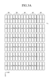
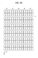
- FIG. 3A and FIG. 3B respectively show pixel arrays of the image display portion during a first period t 1 and a second period t 2 .
- First pixels 30 and second pixels 32 are arranged along a vertical direction of the image display portion 100 (the direction of the Y-axis in FIG. 3A) and are arranged alternately and repeatedly along a horizontal direction of the image display portion 100 (the direction of the X-axis in FIG. 3A).
- the first pixels 30 display left eye images L R , L G , and L B corresponding to a left eye image signal
- the second pixels 32 display right eye images R R , R G and R B corresponding to a right eye image signal.
- a first image is displayed on the image display portion during the first period t 1 .
- a driving voltage is applied to the first electrodes 14 at the first connection terminal 14c through the first terminal electrode 14b and the first connection electrode 14a.
- a reference voltage which by way of example may be a ground voltage, is applied to the second electrodes 16 at the second connection terminal 16c through the second connection electrode 16a.
- the reference voltage is also applied to the common electrode 18.
- parallax barrier 200 is a liquid crystal display of a normally white mode of transmission
- portions of the barrier on which the first electrodes 14 are located become light interception portions
- portions of the barrier on which the second electrodes 16 are located become light transmission portions.
- parallax barrier 200 is a liquid crystal display of a normally black mode of transmission
- portions of the barrier on which the first electrodes 14 are located become light transmission portions
- portions of the barrier on which the second electrodes 16 are located become light interception portions.
- the first pixels 30 display right eye images R R , R G , and R B corresponding to a right eye image signal
- the second pixels 32 display left eye images L R , L G , and L B corresponding to a left eye image signal.
- the reference voltage is applied to the first electrodes 14 at the first connection terminal 14c through the first terminal electrode 14b and the first connection electrode 14a.
- the driving voltage is applied to the second electrodes 16 at the second connection terminal 16c through the second connection electrode 16a.
- the reference voltage is applied to the common electrode 18.
- the parallax barrier is a liquid crystal display of a normally white mode of transmission
- portions of the barrier on which the second electrodes 16 are located become the light interception portions
- portions of the barrier on which the first electrodes 14 are located become the light transmission portions.
- the parallax barrier is a liquid crystal display of a normally black mode of transmission
- portions of the barrier on which the second electrodes 16 are located become the light transmission portions
- portions of the barrier on which the first electrodes 14 are located become the light interception portions.
- the left eye of a user sees the image displayed by the first pixels 30 during the first period t 1 and the image displayed by the second pixels 32 during the second period t 2 .
- the right eye of the user sees the image displayed by the second pixels 32 during the first period t 1 and sees the image displayed by the first pixels 30 during the second period t 2 .
- the user can see a three-dimensional image having a resolution that is as fine as a resolution of a two-dimensional image.
- the light interception portions formed during the first period t 1 and the light interception portions formed during the second period t 2 should have light transmittance rates substantially equal to each other in order to provide three-dimensional images that are natural in appearance to the user.
- the light transmission portions formed during the first period t 1 and the light transmission portions formed during the second period t 2 should have light transmittance rates substantially equal to each other.
- the level of the voltage effectively applied at the first electrodes 14 during the first period t 1 and the level of the voltage effectively applied at the second electrodes 16 during the second period t 2 should be substantially equal to each other.
- the paths from the first connection terminal 14c and the second connection terminal 16c to the first and second electrodes 14 and 16, respectively, are different in length from one another.
- the resistance of the first terminal electrode 14b is determined by Formula 1.
- Formula 1 R ⁇ I / A
- R represents electrical resistance of the first terminal electrode 14b
- p represents resistivity of the material of the first terminal electrode 14b
- I represents the length of the first terminal electrode 14b
- A represents the sectional area of the first terminal electrode 14b.
- the first terminal electrode 14b has a relatively large width in order to reduce the resistance R of the first terminal electrode 14b in the first exemplary embodiment of the invention. That is, referring back to Formula 1, the resistance R decreases by increasing the sectional area A of the first terminal electrode 14b.
- a first terminal electrode is formed with a material having a relatively low resistivity p, and the widths of the first terminal electrode, the first electrodes and the second electrodes are configured to be substantially equal to one another.
- the difference between the voltage effectively applied at the first electrodes and the voltage effectively applied at the second electrodes can be reduced.
- the first electrodes and the second electrodes may be formed with transparent ITO, and the first terminal electrode may be formed with a metal having a relatively lower resistivity p, such as silver (Ag), copper (Cu) and the like.
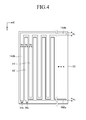
- FIG. 4 shows structures of first electrodes 14' and second electrodes 16' in an electronic display device according to a third exemplary embodiment of the present invention.
- a second connection electrode 162a has a smaller width than a first connection electrode 144b (w 7 ⁇ w 8 ) such that the second connection electrode 162a has a higher electrical resistance than the first connection electrode 144b.
- the relatively higher electrical resistance of the second connection electrode 162a can at least partially match (or compensate) the voltage drop over the first terminal electrode 142b resulting from the electrical resistance of the first terminal electrode 142b.
- the voltages effectively applied at the first electrodes 14' and the second electrodes 16' can be maintained more equally.
- the second connection electrode 162a may be formed with a material that has higher resistivity than a material used to form the first connection electrode 144b while the widths of the second connection electrode 162a and the first connection electrode 144b are kept uniform.
- FIG. 5 is a plan view showing structures of first electrodes 14" and second electrodes 16" in a fourth exemplary embodiment of the present invention.
- an auxiliary connection electrode 166a that lengthens a path along which a voltage is conducted is located between a second connection terminal 16c and a second connection electrode 164a such that voltages effectively applied to the first electrodes 14" and the second electrodes 16" can be maintained more equally.
- a voltage drop resulting over the first terminal electrode 14b is at least partially matched (or compensated) by a voltage drop resulting over the auxiliary connection electrode 166a.
- the length, width, and material of the auxiliary connection electrode 166a can be chosen by considering the magnitude of the voltage drop over the first terminal electrode 14b.
- the shape of the auxiliary connection electrode 166a is not limited to the specific shape shown in FIG. 5. It can also take on various suitable shapes such that the auxiliary connection electrode 166a effectively lengthens the voltage conducting path.
- the steps of decreasing resistance of the first terminal electrode and of increasing resistance of the second connection electrode that are described above may also be used in combination to control the voltage difference.
- the voltage effectively applied to the second electrodes can be reduced by including the auxiliary electrode, as described per the fourth exemplary embodiment.
- the voltage drop over the first electrode can be reduced by widening the width of the first terminal electrode, as described per the first exemplary embodiment.
- FIG. 6 shows third electrodes 34 and fourth electrodes 36 of an electronic display device according to a fifth exemplary embodiment.
- the electronic display device operates the first and second electrodes to separate images when providing a portrait-type view and operates the third and fourth electrodes 34 and 36 to separate images when providing a landscape-type view.
- first electrodes and the second electrodes located on the first substrate of the current exemplary embodiment is substantially similar to the first electrodes and the second electrodes of the first exemplary embodiment, a description of those electrodes is omitted.
- the third electrodes 34 located on the second substrate 12 extend along a first direction (the direction of the X-axis in FIG. 6) perpendicular to the direction along which the first electrodes and the second electrodes extend (see the direction of the Y-axis in FIG. 2, for example). And the third electrodes 34 are arranged along a second direction (the direction of the Y-axis in FIG. 6) in a striped pattern.
- a third connection electrode 34a electrically connecting the third electrodes 34 extends along the second direction, which is perpendicular to the first direction and is connected to respective ends of the third electrodes 34.
- a third connection terminal 34c is formed at an end of the third connection electrode 34a and applies voltage to the third electrodes 34 through the third connection electrode 34a.
- the fourth electrodes 36 extend along the first direction on the second substrate 12.
- the fourth electrodes 36 are located between the third electrodes 34 in a striped pattern.
- a fourth connection electrode 36a electrically connecting the fourth electrodes 36 extends along the second direction and is connected to respective ends of the fourth electrodes 36.
- a fourth terminal electrode 36b extends along the second direction and is connected to an end of the fourth connection electrode 36a.
- a fourth connection terminal 36c is formed at an end of the fourth terminal electrode 36b and applies voltage to the fourth electrodes 36 and the fourth connection electrode 36a through the fourth terminal electrode 36b.
- the width of the fourth terminal electrode 36b w 9 is configured to be greater than respective widths of the third electrodes 34 and the fourth electrodes, w 10 and w 11 .
- the user When the user elects to view the landscape-type view, the user rotates the image display portion and parallax barrier that are oriented to provide the portrait-type view by 90 degrees.
- patterns of pixels displaying left eye and right eye images corresponding to the landscape-type view are formed on the image display portion, and a driving voltage is applied to the third electrodes 34 and the fourth electrodes 36 during operation of the electronic display device.
- an operation providing a landscape-type view in the current exemplary embodiment is substantially similar to the operation providing the portrait-type view in the first exemplary embodiment, a detailed description of the operation providing the landscape-type view is omitted.
- the width of the fourth terminal electrode 36b w 9 is configured to be greater than respective widths of the third electrodes 34 and the fourth electrodes 36, w 10 and w 11 , to decrease electrical resistance of the fourth terminal electrode 36b.
- the fourth terminal electrode may also be formed with a material such as silver (Ag) and copper (Cu) that has a relatively low resistivity in order to further reduce the voltage drop.
- the resistance of the third connection electrode 36a may be increased to reduce the voltage effectively applied to the third electrode (see FIG. 4, for example).
- the width of the third connection electrode 36a may be configured to be smaller than the width of the fourth connection electrode 36a.
- a first terminal electrode was formed with a material used to form a first electrode and a second electrode. Also, the width of the first terminal electrode was configured to be 3.396 times greater than the respective widths of the first electrode and the second electrode.
- An auxiliary connection electrode similar to that described in the fourth exemplary embodiment was formed at an end of a second connection electrode such that a path having an increased electrical resistance was made.
- the first electrode and the second electrode were formed with ITO and had equal widths.
- a first electrode and a second electrode were formed with ITO and had equal widths.
- a first terminal electrode was made of a material also used to form the first electrode and the second electrode and had a width equal to respective widths of the first electrode and the second electrode.
- An auxiliary connection electrode similar to that in the experimental example was not formed at an end of a second connection electrode.
- Other conditions were similar to corresponding conditions that were present in the experimental example.
- FIG. 7A and FIG. 7B show transmission brightness levels of the first electrode and the second electrode, as measured in the comparative example and the experimental example, respectively.
- Table 1 shows measured values of voltages effectively applied at the first electrode and the second electrode.
- Table 1 Comparative example Experimental example applied voltage(V) -1.0 -1.0 First electrode(V) 0.81625 0.57875 second electrode(V) 0.8725 0.575625 Voltage difference (mV) 56.25 3.12
- light transmission rates at each of a plurality of electrodes can be controlled to be substantially equal to each other.
- the present invention provides an electronic display device that can both provide high-resolution three-dimensional images and prevent deterioration of the quality of the three-dimensional images caused by a voltage drop over at least one of the electrodes.
Landscapes
- Engineering & Computer Science (AREA)
- Multimedia (AREA)
- Signal Processing (AREA)
- Liquid Crystal (AREA)
- Stereoscopic And Panoramic Photography (AREA)
- Testing, Inspecting, Measuring Of Stereoscopic Televisions And Televisions (AREA)
Priority Applications (1)
| Application Number | Priority Date | Filing Date | Title |
|---|---|---|---|
| EP20140184352 EP2816804A3 (de) | 2005-11-30 | 2006-11-30 | Elektronische Anzeigevorrichtung |
Applications Claiming Priority (1)
| Application Number | Priority Date | Filing Date | Title |
|---|---|---|---|
| KR1020050115586A KR100688357B1 (ko) | 2005-11-30 | 2005-11-30 | 입체 영상 표시 장치 |
Related Child Applications (2)
| Application Number | Title | Priority Date | Filing Date |
|---|---|---|---|
| EP20140184352 Division EP2816804A3 (de) | 2005-11-30 | 2006-11-30 | Elektronische Anzeigevorrichtung |
| EP20140184352 Division-Into EP2816804A3 (de) | 2005-11-30 | 2006-11-30 | Elektronische Anzeigevorrichtung |
Publications (3)
| Publication Number | Publication Date |
|---|---|
| EP1793624A2 true EP1793624A2 (de) | 2007-06-06 |
| EP1793624A3 EP1793624A3 (de) | 2008-04-23 |
| EP1793624B1 EP1793624B1 (de) | 2014-10-22 |
Family
ID=37654809
Family Applications (2)
| Application Number | Title | Priority Date | Filing Date |
|---|---|---|---|
| EP06125071.8A Not-in-force EP1793624B1 (de) | 2005-11-30 | 2006-11-30 | Elektronische Anzeigevorrichtung |
| EP20140184352 Withdrawn EP2816804A3 (de) | 2005-11-30 | 2006-11-30 | Elektronische Anzeigevorrichtung |
Family Applications After (1)
| Application Number | Title | Priority Date | Filing Date |
|---|---|---|---|
| EP20140184352 Withdrawn EP2816804A3 (de) | 2005-11-30 | 2006-11-30 | Elektronische Anzeigevorrichtung |
Country Status (5)
| Country | Link |
|---|---|
| US (1) | US7511774B2 (de) |
| EP (2) | EP1793624B1 (de) |
| JP (1) | JP5255755B2 (de) |
| KR (1) | KR100688357B1 (de) |
| CN (1) | CN1976483B (de) |
Cited By (1)
| Publication number | Priority date | Publication date | Assignee | Title |
|---|---|---|---|---|
| GB2457692A (en) * | 2008-02-21 | 2009-08-26 | Sharp Kk | A display device with a plurality of viewing modes |
Families Citing this family (23)
| Publication number | Priority date | Publication date | Assignee | Title |
|---|---|---|---|---|
| KR100719507B1 (ko) * | 2005-12-22 | 2007-05-17 | 삼성에스디아이 주식회사 | 입체 영상 표시 장치의 구동 방법 |
| JP4232807B2 (ja) * | 2006-09-06 | 2009-03-04 | セイコーエプソン株式会社 | 電気光学装置及び電子機器 |
| KR100927720B1 (ko) * | 2007-08-24 | 2009-11-18 | 삼성모바일디스플레이주식회사 | 전자 영상 기기 |
| JP2010276817A (ja) * | 2009-05-28 | 2010-12-09 | Seiko Epson Corp | 電気光学装置、および電子機器 |
| US8964013B2 (en) * | 2009-12-31 | 2015-02-24 | Broadcom Corporation | Display with elastic light manipulator |
| US9247286B2 (en) | 2009-12-31 | 2016-01-26 | Broadcom Corporation | Frame formatting supporting mixed two and three dimensional video data communication |
| US8823782B2 (en) * | 2009-12-31 | 2014-09-02 | Broadcom Corporation | Remote control with integrated position, viewer identification and optical and audio test |
| US8854531B2 (en) | 2009-12-31 | 2014-10-07 | Broadcom Corporation | Multiple remote controllers that each simultaneously controls a different visual presentation of a 2D/3D display |
| TWM388658U (en) * | 2010-04-12 | 2010-09-11 | Chunghwa Picture Tubes Ltd | Liquid crystal lens |
| TWM396974U (en) * | 2010-05-21 | 2011-01-21 | Chunghwa Picture Tubes Ltd | Displaying apparatus for switching displaying modes |
| TWI439730B (zh) | 2010-07-16 | 2014-06-01 | Au Optronics Corp | 視差控制元件及其應用 |
| KR101695819B1 (ko) | 2010-08-16 | 2017-01-13 | 엘지전자 주식회사 | 입체영상 디스플레이 장치 및 입체영상 디스플레이 방법 |
| TW201217833A (en) * | 2010-10-27 | 2012-05-01 | Chunghwa Picture Tubes Ltd | Parallax barrier, method of adjusting parallax barrier transmittance and 3D display |
| CN102062977A (zh) * | 2010-11-09 | 2011-05-18 | 华映视讯(吴江)有限公司 | 视差光栅、调整视差光栅之透光率的方法与立体显示器 |
| JP5378342B2 (ja) * | 2010-11-15 | 2013-12-25 | 株式会社ジャパンディスプレイ | 表示装置 |
| CN102636893A (zh) * | 2011-02-09 | 2012-08-15 | 瀚宇彩晶股份有限公司 | 立体显示器、屏障装置及其驱动方法 |
| JP2012226161A (ja) * | 2011-04-20 | 2012-11-15 | Sony Corp | 表示装置 |
| KR101475107B1 (ko) * | 2011-11-16 | 2014-12-23 | 엘지디스플레이 주식회사 | 입체 영상 표시장치 |
| TWI456261B (zh) * | 2011-11-30 | 2014-10-11 | Au Optronics Corp | 立體顯示器及其視差屏障面板 |
| CN102789061B (zh) * | 2012-08-10 | 2014-04-02 | 京东方科技集团股份有限公司 | 视差挡板及显示装置 |
| GB2508844A (en) * | 2012-12-12 | 2014-06-18 | Sharp Kk | Analogue parallax barrier |
| TWI519823B (zh) * | 2013-08-29 | 2016-02-01 | 中華映管股份有限公司 | 立體顯示面板與應用其之對位方法與立體顯示方法 |
| KR102193561B1 (ko) | 2014-03-06 | 2020-12-23 | 삼성디스플레이 주식회사 | 입체영상 표시 장치 |
Citations (4)
| Publication number | Priority date | Publication date | Assignee | Title |
|---|---|---|---|---|
| JPH0572563A (ja) | 1991-09-10 | 1993-03-26 | Rohm Co Ltd | 液晶表示装置 |
| US6137456A (en) | 1996-07-01 | 2000-10-24 | Corning Incorporated | Electronic display device for simultaneously displaying 2D and 3D images |
| JP2003005670A (ja) | 2001-06-20 | 2003-01-08 | Toshiba Corp | 平面表示装置 |
| JP2005134663A (ja) | 2003-10-30 | 2005-05-26 | Asahi Glass Co Ltd | 多機能表示装置および同装置に用いられるスリットマスク形成用のスイッチング液晶パネル |
Family Cites Families (19)
| Publication number | Priority date | Publication date | Assignee | Title |
|---|---|---|---|---|
| JPS5320794A (en) * | 1976-08-10 | 1978-02-25 | Sharp Corp | Electrode structure of display unit |
| JPS55151621A (en) | 1979-05-16 | 1980-11-26 | Hitachi Ltd | Liquid crystal display element |
| JPS5854089B2 (ja) | 1979-06-22 | 1983-12-02 | 株式会社日立製作所 | 透明導電膜の形成方法 |
| JPS63128394A (ja) * | 1986-11-18 | 1988-05-31 | 株式会社東芝 | 表示装置 |
| JPS63140509U (de) | 1987-03-06 | 1988-09-16 | ||
| JP2695887B2 (ja) * | 1989-01-06 | 1998-01-14 | 株式会社日立製作所 | 液晶表示素子 |
| JPH05232403A (ja) * | 1992-02-20 | 1993-09-10 | Ricoh Co Ltd | 表示装置 |
| JPH0611721A (ja) * | 1992-06-26 | 1994-01-21 | Sharp Corp | 液晶パネルの実装構造および実装方法 |
| JP2966781B2 (ja) * | 1995-11-16 | 1999-10-25 | 三洋電機株式会社 | 立体画像表示装置の制御方法 |
| TW393582B (en) | 1995-12-05 | 2000-06-11 | Matsushita Electric Industrial Co Ltd | Backlighting device and color display device |
| KR980010482A (ko) * | 1996-07-01 | 1998-04-30 | 알프레드 엘. 미첼슨 | 자동입체 디스플레이를 생성하도록 인포메이션 디스플레이를 통하여 광 패턴을 전도하기 위한 장치 및 그 방법 |
| JP2000187451A (ja) * | 1998-12-22 | 2000-07-04 | Fujitsu Ltd | ディスプレイ装置の配線設計方法及びその方法を利用したディスプレイ装置 |
| KR20010011108A (ko) * | 1999-07-26 | 2001-02-15 | 김순택 | 입체 영상 디스플레이 장치 |
| KR100806808B1 (ko) * | 2000-10-17 | 2008-02-22 | 엘지.필립스 엘시디 주식회사 | 등저항 배선을 위한 액정표시장치 |
| JP2004014798A (ja) * | 2002-06-06 | 2004-01-15 | Toshiba Corp | パターンレイアウト方法、その装置およびパターンレイアウトプログラムを記憶した媒体 |
| TWI277769B (en) * | 2003-03-25 | 2007-04-01 | Sanyo Electric Co | The stereoscopic video display device and its manufacturing method |
| TW583446B (en) * | 2003-05-28 | 2004-04-11 | Chunghwa Picture Tubes Ltd | Conducting line structure of a liquid crystal display |
| KR20050104649A (ko) * | 2004-04-29 | 2005-11-03 | 삼성에스디아이 주식회사 | 전자 방출 표시장치 |
| KR100728112B1 (ko) * | 2005-03-04 | 2007-06-13 | 삼성에스디아이 주식회사 | 배리어 장치, 이를 이용한 입체영상 표시장치 및 그의 구동방법 |
-
2005
- 2005-11-30 KR KR1020050115586A patent/KR100688357B1/ko not_active Expired - Fee Related
-
2006
- 2006-07-14 JP JP2006194759A patent/JP5255755B2/ja not_active Expired - Fee Related
- 2006-10-20 US US11/584,047 patent/US7511774B2/en not_active Expired - Fee Related
- 2006-11-28 CN CN2006101459424A patent/CN1976483B/zh not_active Expired - Fee Related
- 2006-11-30 EP EP06125071.8A patent/EP1793624B1/de not_active Not-in-force
- 2006-11-30 EP EP20140184352 patent/EP2816804A3/de not_active Withdrawn
Patent Citations (4)
| Publication number | Priority date | Publication date | Assignee | Title |
|---|---|---|---|---|
| JPH0572563A (ja) | 1991-09-10 | 1993-03-26 | Rohm Co Ltd | 液晶表示装置 |
| US6137456A (en) | 1996-07-01 | 2000-10-24 | Corning Incorporated | Electronic display device for simultaneously displaying 2D and 3D images |
| JP2003005670A (ja) | 2001-06-20 | 2003-01-08 | Toshiba Corp | 平面表示装置 |
| JP2005134663A (ja) | 2003-10-30 | 2005-05-26 | Asahi Glass Co Ltd | 多機能表示装置および同装置に用いられるスリットマスク形成用のスイッチング液晶パネル |
Cited By (1)
| Publication number | Priority date | Publication date | Assignee | Title |
|---|---|---|---|---|
| GB2457692A (en) * | 2008-02-21 | 2009-08-26 | Sharp Kk | A display device with a plurality of viewing modes |
Also Published As
| Publication number | Publication date |
|---|---|
| EP2816804A2 (de) | 2014-12-24 |
| EP1793624B1 (de) | 2014-10-22 |
| US20070120768A1 (en) | 2007-05-31 |
| JP5255755B2 (ja) | 2013-08-07 |
| JP2007156415A (ja) | 2007-06-21 |
| KR100688357B1 (ko) | 2007-03-02 |
| EP1793624A3 (de) | 2008-04-23 |
| US7511774B2 (en) | 2009-03-31 |
| CN1976483B (zh) | 2010-11-10 |
| EP2816804A3 (de) | 2015-05-20 |
| CN1976483A (zh) | 2007-06-06 |
Similar Documents
| Publication | Publication Date | Title |
|---|---|---|
| EP1793624B1 (de) | Elektronische Anzeigevorrichtung | |
| EP1802142B1 (de) | Ansteuerungsverfahren einer elektronischen Anzeigevorrichtung | |
| KR100959103B1 (ko) | 입체 영상 표시 장치 및 그 구동 방법 | |
| JP5063296B2 (ja) | 電子映像機器 | |
| US8174564B2 (en) | Three-dimensional display device | |
| KR100728115B1 (ko) | 입체 영상 표시 장치 및 그 구동 방법 | |
| KR100684715B1 (ko) | 입체 영상 표시 장치 및 이를 갖는 전자 기기 | |
| US8823888B2 (en) | Liquid crystal parallax barrier with strip-shaped and step-shaped electrodes and application thereof | |
| JP5160846B2 (ja) | 電子映像機器 | |
| US8395572B2 (en) | Electronic display device | |
| US20130249976A1 (en) | Method for displaying image, image display panel, and image display device | |
| CN110806646B (zh) | 显示面板及其驱动方法、显示装置 | |
| JP2019191214A (ja) | 表示装置およびその製造方法 | |
| US20130265510A1 (en) | Three-dimensional display device and active optical element thereof |
Legal Events
| Date | Code | Title | Description |
|---|---|---|---|
| PUAI | Public reference made under article 153(3) epc to a published international application that has entered the european phase |
Free format text: ORIGINAL CODE: 0009012 |
|
| 17P | Request for examination filed |
Effective date: 20061130 |
|
| AK | Designated contracting states |
Kind code of ref document: A2 Designated state(s): AT BE BG CH CY CZ DE DK EE ES FI FR GB GR HU IE IS IT LI LT LU LV MC NL PL PT RO SE SI SK TR |
|
| AX | Request for extension of the european patent |
Extension state: AL BA HR MK YU |
|
| PUAL | Search report despatched |
Free format text: ORIGINAL CODE: 0009013 |
|
| AK | Designated contracting states |
Kind code of ref document: A3 Designated state(s): AT BE BG CH CY CZ DE DK EE ES FI FR GB GR HU IE IS IT LI LT LU LV MC NL PL PT RO SE SI SK TR |
|
| AX | Request for extension of the european patent |
Extension state: AL BA HR MK RS |
|
| AKX | Designation fees paid |
Designated state(s): DE DK FI FR GB NL |
|
| RAP1 | Party data changed (applicant data changed or rights of an application transferred) |
Owner name: SAMSUNG MOBILE DISPLAY CO., LTD. |
|
| 17Q | First examination report despatched |
Effective date: 20100419 |
|
| RAP1 | Party data changed (applicant data changed or rights of an application transferred) |
Owner name: SAMSUNG DISPLAY CO., LTD. |
|
| REG | Reference to a national code |
Ref country code: DE Ref legal event code: R079 Ref document number: 602006043424 Country of ref document: DE Free format text: PREVIOUS MAIN CLASS: H04N0013000000 Ipc: H04N0013040000 |
|
| GRAP | Despatch of communication of intention to grant a patent |
Free format text: ORIGINAL CODE: EPIDOSNIGR1 |
|
| INTG | Intention to grant announced |
Effective date: 20140612 |
|
| RIC1 | Information provided on ipc code assigned before grant |
Ipc: H04N 13/04 20060101AFI20140603BHEP |
|
| GRAS | Grant fee paid |
Free format text: ORIGINAL CODE: EPIDOSNIGR3 |
|
| GRAA | (expected) grant |
Free format text: ORIGINAL CODE: 0009210 |
|
| AK | Designated contracting states |
Kind code of ref document: B1 Designated state(s): DE DK FI FR GB NL |
|
| REG | Reference to a national code |
Ref country code: GB Ref legal event code: FG4D |
|
| REG | Reference to a national code |
Ref country code: DE Ref legal event code: R096 Ref document number: 602006043424 Country of ref document: DE Effective date: 20141204 |
|
| REG | Reference to a national code |
Ref country code: NL Ref legal event code: VDEP Effective date: 20141022 |
|
| PG25 | Lapsed in a contracting state [announced via postgrant information from national office to epo] |
Ref country code: FI Free format text: LAPSE BECAUSE OF FAILURE TO SUBMIT A TRANSLATION OF THE DESCRIPTION OR TO PAY THE FEE WITHIN THE PRESCRIBED TIME-LIMIT Effective date: 20141022 Ref country code: NL Free format text: LAPSE BECAUSE OF FAILURE TO SUBMIT A TRANSLATION OF THE DESCRIPTION OR TO PAY THE FEE WITHIN THE PRESCRIBED TIME-LIMIT Effective date: 20141022 |
|
| REG | Reference to a national code |
Ref country code: DE Ref legal event code: R097 Ref document number: 602006043424 Country of ref document: DE |
|
| PG25 | Lapsed in a contracting state [announced via postgrant information from national office to epo] |
Ref country code: DK Free format text: LAPSE BECAUSE OF FAILURE TO SUBMIT A TRANSLATION OF THE DESCRIPTION OR TO PAY THE FEE WITHIN THE PRESCRIBED TIME-LIMIT Effective date: 20141022 |
|
| PLBE | No opposition filed within time limit |
Free format text: ORIGINAL CODE: 0009261 |
|
| STAA | Information on the status of an ep patent application or granted ep patent |
Free format text: STATUS: NO OPPOSITION FILED WITHIN TIME LIMIT |
|
| 26N | No opposition filed |
Effective date: 20150723 |
|
| REG | Reference to a national code |
Ref country code: FR Ref legal event code: PLFP Year of fee payment: 10 |
|
| REG | Reference to a national code |
Ref country code: FR Ref legal event code: PLFP Year of fee payment: 11 |
|
| REG | Reference to a national code |
Ref country code: FR Ref legal event code: PLFP Year of fee payment: 12 |
|
| REG | Reference to a national code |
Ref country code: DE Ref legal event code: R079 Ref document number: 602006043424 Country of ref document: DE Free format text: PREVIOUS MAIN CLASS: H04N0013040000 Ipc: H04N0013300000 |
|
| REG | Reference to a national code |
Ref country code: FR Ref legal event code: PLFP Year of fee payment: 13 |
|
| PGFP | Annual fee paid to national office [announced via postgrant information from national office to epo] |
Ref country code: DE Payment date: 20191105 Year of fee payment: 14 |
|
| PGFP | Annual fee paid to national office [announced via postgrant information from national office to epo] |
Ref country code: FR Payment date: 20191107 Year of fee payment: 14 |
|
| PGFP | Annual fee paid to national office [announced via postgrant information from national office to epo] |
Ref country code: GB Payment date: 20191106 Year of fee payment: 14 |
|
| REG | Reference to a national code |
Ref country code: DE Ref legal event code: R119 Ref document number: 602006043424 Country of ref document: DE |
|
| GBPC | Gb: european patent ceased through non-payment of renewal fee |
Effective date: 20201130 |
|
| PG25 | Lapsed in a contracting state [announced via postgrant information from national office to epo] |
Ref country code: FR Free format text: LAPSE BECAUSE OF NON-PAYMENT OF DUE FEES Effective date: 20201130 |
|
| PG25 | Lapsed in a contracting state [announced via postgrant information from national office to epo] |
Ref country code: GB Free format text: LAPSE BECAUSE OF NON-PAYMENT OF DUE FEES Effective date: 20201130 Ref country code: DE Free format text: LAPSE BECAUSE OF NON-PAYMENT OF DUE FEES Effective date: 20210601 |