EP1796171B1 - Flachbildschirm und Herstellungsverfahren dafür - Google Patents
Flachbildschirm und Herstellungsverfahren dafür Download PDFInfo
- Publication number
- EP1796171B1 EP1796171B1 EP06256263.2A EP06256263A EP1796171B1 EP 1796171 B1 EP1796171 B1 EP 1796171B1 EP 06256263 A EP06256263 A EP 06256263A EP 1796171 B1 EP1796171 B1 EP 1796171B1
- Authority
- EP
- European Patent Office
- Prior art keywords
- electrode
- layer
- interconnection
- substrate
- flat panel
- Prior art date
- Legal status (The legal status is an assumption and is not a legal conclusion. Google has not performed a legal analysis and makes no representation as to the accuracy of the status listed.)
- Active
Links
Images



Classifications
-
- H—ELECTRICITY
- H10—SEMICONDUCTOR DEVICES; ELECTRIC SOLID-STATE DEVICES NOT OTHERWISE PROVIDED FOR
- H10D—INORGANIC ELECTRIC SEMICONDUCTOR DEVICES
- H10D86/00—Integrated devices formed in or on insulating or conducting substrates, e.g. formed in silicon-on-insulator [SOI] substrates or on stainless steel or glass substrates
- H10D86/40—Integrated devices formed in or on insulating or conducting substrates, e.g. formed in silicon-on-insulator [SOI] substrates or on stainless steel or glass substrates characterised by multiple TFTs
- H10D86/441—Interconnections, e.g. scanning lines
-
- H—ELECTRICITY
- H10—SEMICONDUCTOR DEVICES; ELECTRIC SOLID-STATE DEVICES NOT OTHERWISE PROVIDED FOR
- H10D—INORGANIC ELECTRIC SEMICONDUCTOR DEVICES
- H10D86/00—Integrated devices formed in or on insulating or conducting substrates, e.g. formed in silicon-on-insulator [SOI] substrates or on stainless steel or glass substrates
- H10D86/40—Integrated devices formed in or on insulating or conducting substrates, e.g. formed in silicon-on-insulator [SOI] substrates or on stainless steel or glass substrates characterised by multiple TFTs
-
- H—ELECTRICITY
- H10—SEMICONDUCTOR DEVICES; ELECTRIC SOLID-STATE DEVICES NOT OTHERWISE PROVIDED FOR
- H10D—INORGANIC ELECTRIC SEMICONDUCTOR DEVICES
- H10D86/00—Integrated devices formed in or on insulating or conducting substrates, e.g. formed in silicon-on-insulator [SOI] substrates or on stainless steel or glass substrates
- H10D86/40—Integrated devices formed in or on insulating or conducting substrates, e.g. formed in silicon-on-insulator [SOI] substrates or on stainless steel or glass substrates characterised by multiple TFTs
- H10D86/451—Integrated devices formed in or on insulating or conducting substrates, e.g. formed in silicon-on-insulator [SOI] substrates or on stainless steel or glass substrates characterised by multiple TFTs characterised by the compositions or shapes of the interlayer dielectrics
-
- H—ELECTRICITY
- H10—SEMICONDUCTOR DEVICES; ELECTRIC SOLID-STATE DEVICES NOT OTHERWISE PROVIDED FOR
- H10D—INORGANIC ELECTRIC SEMICONDUCTOR DEVICES
- H10D86/00—Integrated devices formed in or on insulating or conducting substrates, e.g. formed in silicon-on-insulator [SOI] substrates or on stainless steel or glass substrates
- H10D86/40—Integrated devices formed in or on insulating or conducting substrates, e.g. formed in silicon-on-insulator [SOI] substrates or on stainless steel or glass substrates characterised by multiple TFTs
- H10D86/60—Integrated devices formed in or on insulating or conducting substrates, e.g. formed in silicon-on-insulator [SOI] substrates or on stainless steel or glass substrates characterised by multiple TFTs wherein the TFTs are in active matrices
-
- H—ELECTRICITY
- H10—SEMICONDUCTOR DEVICES; ELECTRIC SOLID-STATE DEVICES NOT OTHERWISE PROVIDED FOR
- H10K—ORGANIC ELECTRIC SOLID-STATE DEVICES
- H10K50/00—Organic light-emitting devices
- H10K50/80—Constructional details
- H10K50/84—Passivation; Containers; Encapsulations
- H10K50/844—Encapsulations
-
- H—ELECTRICITY
- H10—SEMICONDUCTOR DEVICES; ELECTRIC SOLID-STATE DEVICES NOT OTHERWISE PROVIDED FOR
- H10K—ORGANIC ELECTRIC SOLID-STATE DEVICES
- H10K59/00—Integrated devices, or assemblies of multiple devices, comprising at least one organic light-emitting element covered by group H10K50/00
- H10K59/10—OLED displays
- H10K59/12—Active-matrix OLED [AMOLED] displays
- H10K59/124—Insulating layers formed between TFT elements and OLED elements
-
- H—ELECTRICITY
- H10—SEMICONDUCTOR DEVICES; ELECTRIC SOLID-STATE DEVICES NOT OTHERWISE PROVIDED FOR
- H10K—ORGANIC ELECTRIC SOLID-STATE DEVICES
- H10K59/00—Integrated devices, or assemblies of multiple devices, comprising at least one organic light-emitting element covered by group H10K50/00
- H10K59/10—OLED displays
- H10K59/12—Active-matrix OLED [AMOLED] displays
- H10K59/131—Interconnections, e.g. wiring lines or terminals
-
- H—ELECTRICITY
- H10—SEMICONDUCTOR DEVICES; ELECTRIC SOLID-STATE DEVICES NOT OTHERWISE PROVIDED FOR
- H10K—ORGANIC ELECTRIC SOLID-STATE DEVICES
- H10K59/00—Integrated devices, or assemblies of multiple devices, comprising at least one organic light-emitting element covered by group H10K50/00
- H10K59/80—Constructional details
- H10K59/87—Passivation; Containers; Encapsulations
- H10K59/873—Encapsulations
-
- H—ELECTRICITY
- H10—SEMICONDUCTOR DEVICES; ELECTRIC SOLID-STATE DEVICES NOT OTHERWISE PROVIDED FOR
- H10D—INORGANIC ELECTRIC SEMICONDUCTOR DEVICES
- H10D30/00—Field-effect transistors [FET]
- H10D30/60—Insulated-gate field-effect transistors [IGFET]
- H10D30/67—Thin-film transistors [TFT]
- H10D30/6729—Thin-film transistors [TFT] characterised by the electrodes
- H10D30/6737—Thin-film transistors [TFT] characterised by the electrodes characterised by the electrode materials
-
- H—ELECTRICITY
- H10—SEMICONDUCTOR DEVICES; ELECTRIC SOLID-STATE DEVICES NOT OTHERWISE PROVIDED FOR
- H10D—INORGANIC ELECTRIC SEMICONDUCTOR DEVICES
- H10D30/00—Field-effect transistors [FET]
- H10D30/60—Insulated-gate field-effect transistors [IGFET]
- H10D30/67—Thin-film transistors [TFT]
- H10D30/674—Thin-film transistors [TFT] characterised by the active materials
- H10D30/6741—Group IV materials, e.g. germanium or silicon carbide
- H10D30/6743—Silicon
Definitions
- the present invention relates to a flat panel display and a method of fabricating the same.
- Flat panel displays such as a liquid crystal display, an organic light emitting display, an inorganic light emitting display, etc., use aluminum-group metals to reduce interconnection resistance.
- Aluminum-group metal conductors may be readily damaged by an etching solution during a manufacturing process.
- US 2004/0134878 discloses a method for manufacturing a TFT panel of an LCD device that includes the steps of wet etching a multilayer metallic structure including a high-melting-point metal film, Al film and another high-melting-point Smetal film while using side etching technique using a photoresist mask, hot-water washing the side walls of the Al film after the wet etching, and dry etching for configuring the channel region of a TFT in each pixel, and removing the photoresist mask.
- GB 2 396 733 discloses a dual panel-type active matrix organic electroluminescent device that includes a gate line disposed along a first direction on a first substrate, a data line disposed along a second direction on the first substrate, a power line disposed along the second direction on the first substrate and spaced apart from the data line to define a pixel region, with the gate and data lines, the power line and the gate line both formed of a same material during a same process.
- JP 2001 23085 discloses an organic electroluminescence element that includes a transparent positive electrode as a lower side electrode, a hole transporting layer, an organic luminous layer and a negative electrode made of metal as an upper side electrode that are laminated in order on a glass substrate.
- JP 2003 133078 discloses an organic EL element that includes a transparent electrode, a hole transporting layer and a luminescent layer that are laminated in order on a glass base.
- a Ca/Al laminated electrode that comprises two layers of a Ca layer and an Al layer is formed on a part of the luminescent layer.
- the present invention sets out to provide a flat panel display and a method of fabricating the same capable of preventing (or blocking) a conductor such as an electrode, an interconnection, or the like, from being corroded or etched during a manufacturing process. More specifically, the present invention sets out to provide a flat panel display and a method of fabricating the same capable of preventing (or reducing) corrosion and damage of a conductor including an interconnection.
- a first aspect of the invention provides a flat panel display as set out in Claim 1.
- Optional features of this aspect of the invention are set out in Claims 2 to 10.
- a second aspect of the invention provides a method of fabricating a flat panel display as set out in Claim 11.
- Optional features of this aspect of the invention are set out in Claims 12 to 14.
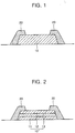
- FIG. 1 is a cross-sectional view of a conductor 10 included in a flat panel display.
- the conductor 10 may be a data interconnection, a scan interconnection, a power interconnection, and/or a bus interconnection for reducing (or preventing) a voltage drop thereof.
- the conductor 10 is used in a flat panel display, or in an electrode of a thin film transistor or a capacitor, as described in more detail below.
- the conductor 10 may include a metal material such as Ag, Mg, Al, Pt, Pd, Au, Ni, Nd, Ir, Cr, Li, Ca, or combinations thereof, and/or a transparent conductive material such as ITO, IZO, ZnO, In 2 O 3 , or combinations thereof.
- a conductive paste including a conductive organic material and/or conductive particles such as Ag, Mg, Cu, etc., may be used.
- the passivation layer pattern 20 is formed of an insulating material to surround the conductor 10, thereby protecting the conductor 10 from an etching solution, etchant, etc., that may permeate to the side surfaces of the conductor 10.
- the passivation layer pattern 20 may be formed of an organic material, which includes at least one selected from the group consisting of polymer derivatives having a phenol group, an acryl-based polymer, an imide-based polymer, an arylether-based polymer, an amide-based polymer, a fluorine-based polymer, a p-silirene-based polymer, a vinyl alcohol-based polymer, and combinations thereof.
- the passivation layer pattern 20 is formed of an acryl-based material.
- the acryl-based material is a photosensitive acryl-based material, thereby facilitating formation of a pattern.
- a conductor 10' formed to have a multi-layered structure including aluminum or an aluminum alloy.
- the conductor 10' includes a first conductive layer 11, a second conductive layer 12, and a third conductive layer 13, which are deposited adjacent to one another (or sequentially deposited).
- the second conductive layer 12 may be formed of aluminum or an aluminum alloy, for example, Al, AlSi, AlNd, AlCu, etc.
- At least one of the first and third conductive layers 11 and 13 may include at least one selected from the group consisting of Cr, a Cr alloy, Mo, a Mo alloy, W, and a W alloy.
- the first and third conductive layers 11 and 13 may be formed of MoW, and the second conductive layer 12 may be formed of AINd.
- the present invention is not thereby limited.
- At least one of the first and third conductive layers 11 and 13 may include at least one selected from the group consisting of Ti, a Ti alloy, Ta, and a Ta alloy.
- the first and third conductive layers 11 and 13 may be formed of a Ti-group metal, and the second conductive layer 12 may be formed of an Al-group metal.
- a passivation layer pattern 20 may be formed of an insulating material to cover a side end of the conductor 10'.
- the passivation layer pattern 20 may be formed of the above-mentioned materials. That is, when the passivation layer pattern 20 is formed of an organic material, the organic material may include at least one selected from the group consisting of polymer derivatives having a phenol group, an acryl-based polymer, an imide-based polymer, an arylether-based polymer, an amide-based polymer, a fluorine-based polymer, a p-silirene-based polymer, a vinyl alcohol-based polymer, and combinations thereof.
- the passivation layer pattern 20 is formed of an acryl-based material.
- the acryl-based material is a photosensitive acryl-based material, thereby facilitating formation of a pattern.
- the conductor 10' is formed in a multi-layered structure, it is possible to improve conductivity of the conductor 10 due to the second conductive layer 12 being in the aluminum-group having a relatively high conductivity, and to protect the second conductive layer 12 using the first and third conductive layers 11 and 13. In addition, it is possible to prevent (or reduce) corrosion and etching of the aluminum-group second conductive layer 12 due to penetration of etchant, etc., using the passivation layer pattern 20 formed on side surfaces of the second conductive layer 12.
- the above structure can be used in various regions such as outer sides of a pixel and an emission region of a flat panel display.
- FIG. 3 is a cross-sectional view of an organic light emitting display in accordance with an embodiment of the present invention.
- a thin film transistor (TFT) 40 and an organic light emitting diode (OLED) are disposed on a substrate 31.
- the substrate 31 may be formed of a plastic material such as acryl, polyimide, polycarbonate, polyester, mylar, etc.
- the present invention is not thereby limited.
- the substrate may be formed of a metal foil such as SUS or tungsten, or a glass material.
- An insulating layer 32 such as a barrier layer and/or a buffer layer may be formed on the substrate 31 to prevent (or reduce) diffusion of impurity ions and penetration of moisture or external air, and to planarize a surface thereof.
- An active layer 41 of the thin film transistor 40 is formed on the insulating layer 32 using a semiconductor material, and a gate insulating layer 33 is formed to cover the active layer 41.
- the active layer 41 may be formed of an inorganic semiconductor such as amorphous silicon or polysilicon, or an organic semiconductor, and includes a source region 412, a drain region 413, and a channel region 411 disposed therebetween.
- a gate electrode 42 is disposed on the gate insulating layer 33, and an interlayer insulating layer 34 is formed to cover the gate electrode 42.
- a source electrode 43 and a drain electrode 44 are disposed on the interlayer insulating layer 34, and then a passivation layer (or a passivation layer pattern) 35 is disposed to cover the source and drain electrodes 43 and 44.
- the gate insulating layer 33, the interlayer insulating layer 34, and the passivation layer 35 may be formed of an insulating material of a single-layered or multi-layered structure, and formed of an organic material, an inorganic material, or an organic/inorganic compound.
- the deposition structure of the above thin film transistor 40 is not thereby limited thereto, and various other suitable structures may be employed.
- a first electrode 51 which is an electrode of the organic light emitting diode OLED is formed on the passivation layer 35, and a pixel-defining layer 37 is formed thereon.
- An opening 38 is formed in the pixel-defining layer 37 to expose the first electrode 51, and then an organic layer 52 of the organic light emitting diode OLED is formed.
- the organic light emitting diode OLED emits light of red, green, and blue depending on current flow to display an image information.
- the organic light emitting diode OLED includes the first electrode 51 in contact with a drain electrode 44 of the thin film transistor 40 through a via-hole 36, a second electrode 53 for covering the entire pixel, and an organic layer 52 having an emission layer disposed between the first electrode 51 and the second electrode 53 to emit light.
- the first electrode 51 and the second electrode 53 are insulated from each other by the organic layer 52, and different polarities of voltages are applied to the organic layer 52 to emit light from the organic layer 52.
- the organic layer 52 may use a low molecular organic layer or a polymer organic layer.
- a hole injection layer (HIL), a hole transport layer (HTL), an emission layer (EML), an electron transport layer (ETL), an electron injection layer (EIL), etc. may be deposited in a single or multi-layered structure.
- various organic materials such as copper phthalocyanine (CuPc), N,N-Di(naphthalene-1-yl)-N,N'-diphenyl-benzidine (NPB), tris-8-hydroxyquinoline aluminum (Alq3), or the like, may be employed.
- the low molecular organic layer may be formed by a vacuum deposition method.
- the hole injection layer, the hole transport layer, the electron transport layer, and the electron injection layer may be applied to red, green and blue pixels in common as common layers. Therefore, unlike the embodiment shown in FIG. 3 , the common layers according to one embodiment may be formed to cover the entire pixels, similar to the second electrode 53.
- the polymer organic layer may have a structure including a hole transport layer (HTL) and an emission layer (EML).
- the hole transport layer may be formed of PEDOT
- the emission layer may be formed of a poly-phenylenevinylene(PPV)-based or polyfluorene-based polymer organic material.
- the hole transport layer and the emission layer may be formed by a screen printing method, an inkjet printing method, or the like.
- the organic layer of the present invention is not thereby limited to the organic layer shown in FIG. 3 .
- the first electrode 51 functions as an anode electrode
- the second electrode 53 functions as a cathode electrode.
- the first electrode 51 may function as a cathode electrode
- the second electrode 53 may function as the anode electrode.
- the first electrode 51 may be a transparent electrode
- the second electrode 53 may be a reflective electrode.
- the transparent electrode as the first electrode 51 may be formed of ITO, IZO, In 2 O 3 , ZnO, or the like, having a relatively high work function
- the reflective electrode as the second electrode 53 may be formed of a metal material such as Ag, Mg, Al, Pt, Pd, Au, Ni, Nd, Ir, Cr, Li, Ca, or compounds thereof.
- the first electrode 51 may be a reflective electrode
- the second electrode 53 may be a transparent electrode.
- the reflective electrode as the first electrode 51 may be made by forming a reflective layer using Ag, Mg, Al, Pt, Pd, Au, Ni, Nd, Ir, Cr, Li, Ca, or combinations thereof, and then forming a layer using ITO, IZO, In 2 O 3 , ZnO, or the like, having a relatively high work function.
- the transparent electrode as the second electrode 53 may be made by depositing a metal having a relatively low work function such as Ag, Mg, Al, Pt, Pd, Au, Ni, Nd, Ir, Cr, Li, Ca, or combinations thereof, and then forming an auxiliary electrode layer or a bus electrode line using a transparent conductive material such as ITO, IZO, In 2 O 3 , ZnO, or the like.
- a metal having a relatively low work function such as Ag, Mg, Al, Pt, Pd, Au, Ni, Nd, Ir, Cr, Li, Ca, or combinations thereof.
- both the first and second electrodes 51 and 53 may be formed as transparent electrodes.
- the first and second electrodes 51 and 53 are not limited to the above described materials, and may be formed of a conductive organic material, or a conductive paste including conductive particles such as Ag, Mg, Cu, or the like, in addition to the above described materials.
- the electrodes 51 and 53 may be printed by an inkjet printing method, and then may be plasticized.
- an upper part thereof is sealed (or hermetically sealed) to block the organic light emitting diode OLED from external air.
- the gate electrode 42, the source electrode 43, and the drain electrode 44 may include a metal material such as Ag, Mg, Al, Pt, Pd, Au, Ni, Nd, Ir, Cr, Li, Ca or combinations thereof, or a transparent conductive material such as ITO, IZO, In 2 O 3 , ZnO, or the like.
- a conductive organic material, or a conductive paste including conductive particles such as Ag, Mg, Cu, or the like, may be used.
- the electrodes may be formed in a three-layered structure, as shown in FIG. 2 .
- the gate electrode 42 has a single layered structure, and the source electrode 43 and the drain electrode 44 have a three-layered structure.
- the structure in which the gate electrode 42 has a single layered structure, and the source electrode 43 and the drain electrode 44 have a three-layered structure will be described in more detail.
- the source electrode 43 and the drain electrode 44 may include a structure in which first conductive layers 431 and 441, second conductive layers 432 and 442, and third conductive layers 433 and 443 are sequentially deposited from a lower side of FIG. 3 .
- the second conductive layers 432 and 442 may be formed of aluminum or an aluminum alloy, for example, Al, AlSi, AINd, AlCu, or the like.
- At least one of the first conductive layers 431 and 441 or the third conductive layers 433 and 443 may include at least one selected from the group consisting of Ti, a Ti alloy.
- first conductive layers 431 and 441 and the third conductive layers 433 and 443 may be formed of a Ti-based metal
- second conductive layers 432 and 442 may be formed of an Al-based metal
- a passivation layer pattern 45 is formed to cover side ends of the source electrode 43 and the drain electrode 44 using an insulating material.
- the passivation layer pattern is formed of an organic material, which organic material may be formed of at least one selected from the group consisting of polymer derivatives having a phenol group, an acryl-based polymer, an imide-based polymer, an arylether-based polymer, an amide-based polymer, a fluorine-based polymer, a p-silirene-based polymer, a vinyl alcohol-based polymer, and combinations thereof.
- the passivation layer pattern 45 is formed of an acryl-based material.
- the acryl-based material is a photosensitive acryl-based material, thereby facilitating formation of a pattern.
- the source electrode 43 and the drain source 44 are formed in a multi-layered structure, it is possible to improve conductivity of the source electrode 43 and the drain source 44 due to the second conductive layers 432 and 442 being in the aluminum-group having a relatively high conductivity, and to protect the second conductive layers 432 and 442 using the first conductive layers 431 and 441 and the third conductive layers 433 and 443.
- the first electrode 51 is patterned, it is more advantageous to protect the source electrode 43 and the drain electrode 44 from penetration of the etchant.
- an interconnection 60 may be further formed.
- the interconnection 60 may be a Vdd power line, but is not limited thereto, and various suitable interconnections can be adapted to a pixel circuit of an organic light emitting display.
- the interconnection 60 formed together with the source electrode 43 and the drain electrode 44, also has a first conductive layer 601, a second conductive layer 602, and a third conductive layer 603.
- the first, second and third conductive layers 601, 602 and 603 may be formed of the same materials as the above described conductive layer materials.
- a passivation layer pattern 61 may be formed as described above. That is, since the passivation layer pattern 61 is formed to be substantially the same as passivation layer pattern 45, a detailed description thereof will not be provided.
- a bus line 70 may be disposed in contact with the second electrode 53.
- the bus line 70 formed together with the source and drain electrodes 43 and 44, also has a first conductive layer 701, a second conductive layer 702, and a third conductive layer 703.
- the first, second and third conductive layers 701, 702 and 703 may be formed of the same materials as the above described conductive layer materials.
- the bus line 70 is in contact with the second electrode 53 through a via-hole 39 formed in the passivation layer 35 to allow power to be supplied to the second electrode 53.
- a passivation layer pattern 71 may be formed in substantially the same manner as described above. That is, since the passivation layer pattern 71 is formed in a manner substantially the same as the source and drain electrodes 43 and 44 are formed, a detailed description thereof will not be provided.
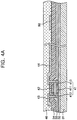
- FIGs. 4A to 4D are cross-sectional views illustrating a method of fabricating an organic light emitting display in accordance with an exemplary embodiment of the present invention.
- an insulating layer 32 is formed on a substrate 31 to prevent (or block) diffusion of impurities such as metal ions from the substrate 31 and penetration into an active layer 41.
- amorphous silicon is deposited and crystallized on the insulating layer 32 to form a polysilicon layer, and then the polysilicon layer is patterned to form the active layer 41.
- a gate insulating layer 33 is deposited on the entire surface of the substrate including the active layer 41, and a gate metal is deposited on the gate insulating layer 33 and patterned to form a gate electrode 42.
- impurities of a predetermined conductivity type are doped into the active layer 41 using the gate electrode 42 as a mask to form source and drain regions 412 and 413.
- an interlayer insulating layer 34 is formed on the entire surface of the substrate, including the active layer 41, and contact holes are formed to expose a portion of the source and drain regions 412 and 413 in the interlayer insulating layer 34.
- a conductive material is deposited on the interlayer insulating layer 34 including the contact holes, and then patterned to form source and drain electrodes 43 and 44 connected to the source and drain regions 412 and 413 through the contact holes, thereby completing the thin film transistor including the active layer 41, the gate electrode 42, and the source and drain electrodes 43 and 44.
- an interconnection 80 is simultaneously formed in a non-emission region of the substrate 31 to electrically connect an external circuit module and the thin film transistor. That is, the interconnection 80 is electrically connected to the TFT and the external circuit module.
- the source and drain electrodes 43 and 44 and the interconnection 80 are formed of a material selected from the group consisting of Ti/Al, Ti/Al alloy (AlSi, AINd, and equivalent thereof), Ti/Al/Ti, Ti/TiN/Al/TiN/Ti, Ti/TiN/AlSi/TiN/Ti, and Ti/Al alloy/Ti.
- a planarization layer 46 is formed on the substrate including the source and drain electrodes 43 and 44 and the interconnection 80 to complete a TFT panel.
- the planarization layer 46 may be formed of a material selected from the group consisting of acryl, polyimide (PI), benzocyclobutene (BCB), silicate-on-glass (SOG), and equivalents thereof, to remove a step of a lower structure.
- the planarization layer 46 may be formed by spin-coating and/or slit-coating the material.
- the planarization layer 46 is formed, and then patterned to form a via-hole 36 exposing a portion of one of the source and drain electrodes 43 and 44, for example, the drain electrode 44.
- a passivation layer pattern 81 having an opening 81a exposing a portion of the interconnection 80 and disposed on a side end of the interconnection 80 is simultaneously formed.
- the first electrode 51 may be formed of a transparent or semitransparent conductive layer.
- the first electrode 51 may include one or more layers formed by a material selected from the group consisting of ITO, IZO, ITZO, and equivalents thereof, i.e., metal oxide having indium.
- the first electrode 51 may include a structure having ITO(or IZO, ITZO)/Al(or Al alloy), ITO(or IZO, ITZO)/Al(or Al alloy)/ITO(or IZO, ITZO), or the like.
- a pixel-defining layer 37 is deposited on the entire surface of the substrate including the first electrode 51 and patterned to form an opening 38 exposing a portion of the first electrode 51.
- the pixel-defining layer 37 disposed in a non-emission region of the substrate 31 is also removed.
- an organic layer 52 including an emission layer is formed on the pixel-defining layer 37 including the opening 38.
- the organic layer 52 may be composed of various layers according to its function.
- the organic layers include a hole injection layer (HIL), a hole transport layer (HTL), an emission layer (EML), a hole blocking layer (HBL), an electron transport layer (ETL), and/or an electron injection layer (EIL), in addition to the emission layer.
- HIL hole injection layer
- HTL hole transport layer
- EML emission layer
- HBL hole blocking layer
- ETL electron transport layer
- EIL electron injection layer
- the organic layer 52 is formed of forming a hole injection layer (HIL), a hole transport layer (HTL), and so on, forming an emission layer (EML) in the opening, and then forming a hole blocking layer (HBL), an electron transport layer (ETL), and an electron injection layer (EIL).
- HIL hole injection layer
- HTL hole transport layer
- EML emission layer
- HBL hole blocking layer
- ETL electron transport layer
- EIL electron injection layer
- a second electrode 53 is formed on the organic layer 52 to complete an organic light emitting diode including the first electrode 51, the organic layer 52, and the second electrode 53.
- An encapsulation substrate can then be mounted on the organic light emitting diode to encapsulate the substrate 31, on which the TFT and the organic light emitting diode are formed, using sealant, and then the metal interconnection 80 is electrically connected to an external circuit module, thereby completing the organic light emitting display according to the embodiment of the present invention.
- An organic light emitting display in accordance with the present invention includes the source and drain electrodes 43 and 44 and the interconnection 80 formed of at least one selected from the group consisting of Ti/Al, Ti/Al alloy(AlSi, AINd, and equivalent thereof), Ti/Al/Ti, Ti/TiN/Al/TiN/Ti, Ti/TiN/AlSi/TiN/Ti, and Ti/Al alloy/Ti, thereby improving corrosion resistance of the metal interconnection 80 against external environment.
- the first electrode 51 is generally formed by patterning through wet etching. Since the interconnection 80 is formed by the deposition layer as described above and a side end of the interconnection 80 is protected by the passivation layer pattern 81, it is possible to prevent (or reduce) damage of the interconnection 80 caused by the wet etching.
- an embodiment of the present invention provides an organic light emitting display and a method of fabricating the same capable of improving corrosion resistance of a metal interconnection in a non-emission region of a TFT panel.
Landscapes
- Engineering & Computer Science (AREA)
- Microelectronics & Electronic Packaging (AREA)
- Physics & Mathematics (AREA)
- Optics & Photonics (AREA)
- Electroluminescent Light Sources (AREA)
- Devices For Indicating Variable Information By Combining Individual Elements (AREA)
- Internal Circuitry In Semiconductor Integrated Circuit Devices (AREA)
- Thin Film Transistor (AREA)
Claims (14)
- Flachbildschirm, umfassend:einen Dünnschichttransistor auf einem Substrat und mit einer Source-Elektrode (43) und einer Drain-Elektrode (44);eine Verbindung (80), die auf dem Substrat in einem Nichtemissionsbereich des Substrats (31) angeordnet und elektrisch mit dem Dünnschichttransistor verbunden ist;eine Planarisierungsschicht (46), die aus einem organischen dielektrischen Material ausgebildet und auf dem Substrat vorgesehen ist, um den Dünnschichttransistor (41, 42) und die Verbindung (80) zumindest teilweise abzudecken, wobei die Planarisierungsschicht (46) eine Durchkontaktierung umfasst, die einen Abschnitt der Source-Elektrode oder der Drain-Elektrode (44) freilegt, wobei die Planarisierungsschicht (46) ferner eine Öffnung (81) umfasst, die einen Abschnitt der Verbindung (80) freilegt und an einem seitlichen Ende der Verbindung (80) angeordnet ist, wodurch eine Passivierungsschichtstruktur (81) auf der Verbindung (80) ausgebildet wird; undeine organische lichtemittierende Diode, die elektrisch mit dem Dünnschichttransistor verbunden ist;dadurch gekennzeichnet, dassdie Source-Elektrode (43), die Drain-Elektrode (44) und die Verbindung (80) aus dem gleichen Materialstapel ausgebildet sind, der ausgewählt ist aus der Gruppe bestehend aus Ti/Al, Ti/Al-Legierung, Ti/Al/Ti, Ti/TiN/Al/TiN/Ti, Ti/TiN/AlSi/TiN/Ti und Ti/Al-Legierung/Ti.
- Flachbildschirm nach Anspruch 1, wobei die Al-Legierung ein Material umfasst, das ausgewählt ist aus der Gruppe bestehend aus AlSi und AlNd.
- Flachbildschirm nach Anspruch 1 oder 2, wobei die organische lichtemittierende Diode eine erste Elektrode, eine zweite Elektrode und eine zwischen der ersten Elektrode und der zweiten Elektrode angeordnete organische Schicht umfasst, wobei die organische Schicht eine Emissionsschicht aufweist; und die Verbindung elektrisch mit der organischen lichtemittierenden Diode verbunden ist.
- Flachbildschirm nach Anspruch 3, wobei die Verbindung elektrisch mit der zweiten Elektrode der organischen lichtemittierenden Diode verbunden ist.
- Flachbildschirm nach Anspruch 3, wobei die Verbindung eine Stromverbindung ist, die elektrisch mit der organischen lichtemittierenden Diode verbunden ist.
- Flachbildschirm nach Anspruch 3, wobei die Verbindung eine Signalverbindung ist, die elektrisch mit der organischen lichtemittierenden Diode verbunden ist.
- Flachbildschirm nach einem vorhergehenden Anspruch, wobei die Planarisierungsschicht und die Passivierungsschichtstruktur aus einem Material ausgebildet sind, das ausgewählt ist aus der Gruppe bestehend aus Acryl, Polyimid (PI) und Benzocyclobuten (BCB).
- Flachbildschirm nach Anspruch 1, wobei die organische lichtemittierende Diode Folgendes umfasst:eine erste Elektrode, die elektrisch mit der Source-Elektrode oder der Drain-Elektrode des Dünnschichttransistors verbunden ist;eine pixeldefinierende Schicht, die eine Öffnung umfasst, die einen Abschnitt der ersten Elektrode freilegt;eine organische Schicht, die eine Emissionsschicht umfasst, die auf der ersten Elektrode angeordnet ist, die durch die Öffnung freigelegt wird; undeine zweite Elektrode, die auf der organischen Schicht angeordnet ist.
- Flachbildschirm nach Anspruch 8, wobei die erste Elektrode aus einer oder mehreren Schichten ausgebildet ist, die ein Indium umfassendes Metalloxid umfassen.
- Flachbildschirm nach Anspruch 1, wobei der Dünnschichttransistor ferner Folgendes umfasst:eine aktive Schicht (41), die auf dem Substrat (31) angeordnet ist und einen Source-Bereich, einen Kanalbereich und einen Drain-Bereich umfasst;eine Gate-Isolierschicht (33), die auf dem Substrat (31) angeordnet ist, um zumindest die aktive Schicht (41) abzudecken;eine Gate-Elektrode (42), die auf einem Bereich der Gate-Isolierschicht (33) angeordnet ist, welcher der aktiven Schicht (41) entspricht; undeine Zwischenschicht-Isolierschicht (34), die auf dem Substrat (31) angeordnet ist, um zumindest die Gate-Elektrode (42) abzudecken,wobei die Source-Elektrode und die Drain-Elektrode (43, 44) auf der Zwischenschicht-Isolierschicht (34) angeordnet und elektrisch entsprechend mit dem Source-Bereich und dem Drain-Bereich verbunden sind, und wobei die Verbindung (80) auf der gleichen Schicht wie die Source-Elektrode und die Drain-Elektrode (43, 44) angeordnet ist.
- Verfahren zur Herstellung eines Flachbildschirms, wobei das Verfahren Folgendes umfasst:Ausbilden eines Dünnschichttransistors mit einer Source-Elektrode (43) und einer Drain-Elektrode (44) auf einem Substrat (31);Ausbilden einer Verbindung (80) auf dem Substrat (31) und in einem Nichtemissionsbereich des Substrats (31), wobei die Verbindung gleichzeitig mit der Source-Elektrode (43) und der Drain-Elektrode (44) aus dem gleichen Materialstapel ausgebildet und elektrisch mit dem Dünnschichttransistor auf dem Substrat (31) verbunden wird;Ausbilden einer Planarisierungsschicht (46), die aus einem organischen Material ausgebildet ist, auf dem Substrat (31), um zumindest den Dünnschichttransistor und die Verbindung (80) abzudecken;Strukturieren der Planarisierungsschicht (46), um gleichzeitig eine Durchkontaktierung auszubilden, die einen Abschnitt der Source-Elektrode (43) oder der Drain-Elektrode (44) freilegt, undFreilegen eines Abschnitts der Verbindung (80), um eine Passivierungsschichtstruktur (81) auszubilden, die an einem seitlichen Ende der Verbindung (80) angeordnet ist; undAusbilden einer organischen lichtemittierenden Diode, die elektrisch mit der Source-Elektrode (43) und der Drain-Elektrode (44) verbunden ist;dadurch gekennzeichnet, dassdie Source-Elektrode (43), die Drain-Elektrode (44) und die Verbindung (80) aus einem Materialstapel ausgebildet sind, der ausgewählt ist aus der Gruppe bestehend aus Ti/Al, Ti/Al-Legierung, Ti/Al/Ti, Ti/TiN/Al/TiN/Ti, Ti/TiN/AlSi/TiN/Ti und Ti/Al-Legierung/Ti.
- Verfahren nach Anspruch 11, wobei die Al-Legierung ein Material umfasst, das ausgewählt ist aus der Gruppe bestehend aus AlSi und AlNd.
- Verfahren nach Anspruch 11 oder 12, wobei die Planarisierungsschicht und die Passivierungsschichtstruktur aus einem Material ausgebildet sind, das ausgewählt ist aus der Gruppe bestehend aus Acryl, Polyimid (PI) und Benzocyclobuten (BCB).
- Verfahren nach einem der Ansprüche 11 bis 13, wobei die Planarisierungsschicht durch Rotationsbeschichten oder Schlitzdüsenbeschichten ausgebildet wird.
Applications Claiming Priority (2)
| Application Number | Priority Date | Filing Date | Title |
|---|---|---|---|
| KR1020050120759A KR100685841B1 (ko) | 2005-12-09 | 2005-12-09 | 유기 전계 발광 표시 장치 및 그의 제조 방법 |
| KR1020050123994A KR100777728B1 (ko) | 2005-12-15 | 2005-12-15 | 평판 표시 장치 |
Publications (3)
| Publication Number | Publication Date |
|---|---|
| EP1796171A2 EP1796171A2 (de) | 2007-06-13 |
| EP1796171A3 EP1796171A3 (de) | 2010-10-20 |
| EP1796171B1 true EP1796171B1 (de) | 2019-11-27 |
Family
ID=37888269
Family Applications (1)
| Application Number | Title | Priority Date | Filing Date |
|---|---|---|---|
| EP06256263.2A Active EP1796171B1 (de) | 2005-12-09 | 2006-12-08 | Flachbildschirm und Herstellungsverfahren dafür |
Country Status (5)
| Country | Link |
|---|---|
| US (2) | US8203264B2 (de) |
| EP (1) | EP1796171B1 (de) |
| JP (1) | JP4974661B2 (de) |
| CN (1) | CN104201186B (de) |
| TW (1) | TWI339442B (de) |
Families Citing this family (53)
| Publication number | Priority date | Publication date | Assignee | Title |
|---|---|---|---|---|
| KR100936874B1 (ko) * | 2007-12-18 | 2010-01-14 | 삼성모바일디스플레이주식회사 | 박막 트랜지스터의 제조 방법 및 박막 트랜지스터를구비하는 유기전계발광 표시 장치의 제조 방법 |
| US8344387B2 (en) | 2008-11-28 | 2013-01-01 | Semiconductor Energy Laboratory Co., Ltd. | Semiconductor device and method for manufacturing the same |
| KR101073552B1 (ko) * | 2009-10-09 | 2011-10-17 | 삼성모바일디스플레이주식회사 | 유기 발광 표시 장치 및 그 제조 방법 |
| CN102640279B (zh) * | 2009-10-30 | 2015-06-17 | 株式会社半导体能源研究所 | 半导体器件 |
| KR101094290B1 (ko) * | 2010-01-18 | 2011-12-19 | 삼성모바일디스플레이주식회사 | 유기 발광 표시 장치 |
| KR20110110589A (ko) * | 2010-04-01 | 2011-10-07 | 삼성모바일디스플레이주식회사 | 유기 발광 소자 |
| KR20120078954A (ko) * | 2011-01-03 | 2012-07-11 | 삼성모바일디스플레이주식회사 | 유기전계발광표시장치 및 그 제조방법 |
| KR20120131753A (ko) * | 2011-05-26 | 2012-12-05 | 삼성디스플레이 주식회사 | 박막 트랜지스터, 박막 트랜지스터의 제조 방법 및 유기 발광 표시 장치 |
| JP5861187B2 (ja) * | 2011-07-05 | 2016-02-16 | 株式会社Joled | 有機el素子およびその製造方法 |
| KR101811027B1 (ko) * | 2011-07-07 | 2017-12-21 | 삼성디스플레이 주식회사 | 유기 발광 디스플레이 장치 |
| US8912547B2 (en) * | 2012-01-20 | 2014-12-16 | Semiconductor Energy Laboratory Co., Ltd. | Light-emitting device, display device, and semiconductor device |
| KR101306192B1 (ko) * | 2012-02-10 | 2013-10-16 | 서울대학교산학협력단 | 유기 발광 소자의 제조 방법 및 그에 의한 유기 발광 소자 |
| US20130207102A1 (en) * | 2012-02-15 | 2013-08-15 | Semiconductor Energy Laboratory Co., Ltd. | Semiconductor device |
| CN103367454A (zh) * | 2012-03-31 | 2013-10-23 | 联胜(中国)科技有限公司 | 薄膜晶体管、其制作方法及应用其的主动矩阵显示面板 |
| KR101959976B1 (ko) * | 2012-05-16 | 2019-03-21 | 삼성디스플레이 주식회사 | 표시 장치 및 표시 장치의 단락 불량 검출 방법 |
| KR102090703B1 (ko) * | 2013-05-21 | 2020-04-16 | 삼성디스플레이 주식회사 | 유기발광표시장치 및 그 제조방법 |
| KR102098741B1 (ko) * | 2013-05-27 | 2020-04-09 | 삼성디스플레이 주식회사 | 증착용 기판 이동부, 이를 포함하는 유기층 증착 장치 및 이를 이용한 유기 발광 디스플레이 장치의 제조 방법 |
| KR102199696B1 (ko) * | 2013-11-25 | 2021-01-08 | 엘지디스플레이 주식회사 | 어레이 기판 및 이의 제조방법 |
| KR102169013B1 (ko) * | 2013-12-17 | 2020-10-23 | 삼성디스플레이 주식회사 | 박막트랜지스터 어레이 기판, 유기 발광 표시 장치 및 박막트랜지스터 어레이 기판의 제조 방법 |
| KR102210210B1 (ko) * | 2014-01-06 | 2021-02-02 | 삼성디스플레이 주식회사 | 유기 발광 표시 장치 |
| TWM505004U (zh) * | 2014-04-14 | 2015-07-11 | Ind Tech Res Inst | 觸控面板 |
| US10411078B2 (en) | 2014-04-14 | 2019-09-10 | Industrial Technology Research Institute | Sensing display apparatus |
| KR20150137214A (ko) * | 2014-05-28 | 2015-12-09 | 삼성디스플레이 주식회사 | 유기발광 디스플레이 장치 및 그 제조방법 |
| US10181573B2 (en) | 2014-07-11 | 2019-01-15 | Lg Display Co., Ltd. | Organic light-emitting diode display device and method of fabricating the same |
| US20160018710A1 (en) * | 2014-07-21 | 2016-01-21 | Li Chai | Display panel, array substrate and method for manufacturing the same |
| KR20160081101A (ko) | 2014-12-30 | 2016-07-08 | 삼성디스플레이 주식회사 | 유기 발광 표시 장치의 제조 방법 및 상기 제조 방법에 의해 제조된 유기 발광 표시 장치 |
| KR102339284B1 (ko) * | 2014-12-30 | 2021-12-15 | 삼성디스플레이 주식회사 | 유기 발광 표시 장치의 제조 방법 및 상기 제조 방법에 의해 제조된 유기 발광 표시 장치 |
| KR102411327B1 (ko) * | 2015-01-02 | 2022-06-21 | 삼성디스플레이 주식회사 | 표시 장치 |
| TWI651574B (zh) * | 2015-01-12 | 2019-02-21 | 友達光電股份有限公司 | 顯示面板及其製造方法 |
| KR102545253B1 (ko) * | 2015-05-28 | 2023-06-19 | 엘지디스플레이 주식회사 | 유기 발광 표시 장치 및 그 제조 방법 |
| KR102561113B1 (ko) | 2015-08-13 | 2023-07-28 | 삼성디스플레이 주식회사 | 유기 발광 표시 장치 및 그 제조 방법 |
| KR102571085B1 (ko) * | 2016-04-04 | 2023-08-28 | 삼성디스플레이 주식회사 | 디스플레이 장치 |
| KR102493128B1 (ko) | 2016-04-12 | 2023-01-31 | 삼성디스플레이 주식회사 | 박막트랜지스터 기판, 이를 포함하는 표시 장치 및 그 제조 방법 |
| KR102553981B1 (ko) * | 2016-08-16 | 2023-07-12 | 삼성디스플레이 주식회사 | 표시 장치용 백플레인 및 이의 제조 방법 |
| KR102593455B1 (ko) * | 2016-09-29 | 2023-10-25 | 엘지디스플레이 주식회사 | 유기전계발광표시장치 |
| CN107957799B (zh) * | 2016-10-14 | 2021-08-10 | 群创光电股份有限公司 | 触控显示面板 |
| KR102781934B1 (ko) | 2016-12-30 | 2025-03-19 | 삼성디스플레이 주식회사 | 도전 패턴 및 이를 구비하는 표시 장치 |
| KR102752841B1 (ko) * | 2016-12-30 | 2025-01-10 | 엘지디스플레이 주식회사 | 유기 발광 표시 장치 및 그 제조 방법 |
| KR101921627B1 (ko) | 2017-06-16 | 2018-11-26 | 한국과학기술연구원 | 전계 효과 트랜지스터, 이를 구비한 바이오 센서, 전계 효과 트랜지스터의 제조방법 및 바이오 센서의 제조방법 |
| KR102519087B1 (ko) * | 2017-06-30 | 2023-04-05 | 엘지디스플레이 주식회사 | 표시 장치 및 이의 제조 방법 |
| JP2019070768A (ja) * | 2017-10-11 | 2019-05-09 | シャープ株式会社 | アレイ基板およびその製造方法、並びに表示パネル |
| CN107658333A (zh) * | 2017-10-31 | 2018-02-02 | 京东方科技集团股份有限公司 | 一种柔性显示面板及其制造方法、柔性显示装置 |
| KR102503788B1 (ko) * | 2017-11-21 | 2023-02-27 | 삼성디스플레이 주식회사 | 식각액 조성물 및 이를 이용한 디스플레이 장치의 제조방법 |
| KR102637849B1 (ko) * | 2017-11-28 | 2024-02-19 | 삼성디스플레이 주식회사 | 도전 패턴, 이를 포함하는 표시장치 및 도전 패턴의 제조 방법 |
| CN111972043B (zh) * | 2018-03-29 | 2023-08-01 | 夏普株式会社 | 显示装置及其制造方法 |
| CN109100893B (zh) * | 2018-06-29 | 2021-11-09 | 武汉华星光电技术有限公司 | 显示面板及其制备方法、阵列基板 |
| CN109065455A (zh) * | 2018-08-03 | 2018-12-21 | 深圳市华星光电半导体显示技术有限公司 | 薄膜晶体管的制备方法及采用该方法制备的薄膜晶体管 |
| US11957015B2 (en) * | 2018-09-25 | 2024-04-09 | Sharp Kabushiki Kaisha | Display device |
| KR102075741B1 (ko) | 2018-12-17 | 2020-02-10 | 엘지디스플레이 주식회사 | 표시패널 |
| CN110335886A (zh) * | 2019-06-21 | 2019-10-15 | 武汉华星光电半导体显示技术有限公司 | 阵列基板 |
| KR102349278B1 (ko) | 2019-09-03 | 2022-01-11 | 삼성디스플레이 주식회사 | 유기 발광 소자 |
| CN113644097B (zh) * | 2021-07-27 | 2023-12-22 | 昆山国显光电有限公司 | 显示面板、电子设备和显示面板的制作方法 |
| KR20240074298A (ko) * | 2022-11-21 | 2024-05-28 | 엘지디스플레이 주식회사 | 표시 장치 |
Family Cites Families (36)
| Publication number | Priority date | Publication date | Assignee | Title |
|---|---|---|---|---|
| JPS5270751A (en) | 1975-12-09 | 1977-06-13 | Fujitsu Ltd | Manufacture of electrode of gas discharge panel |
| JPS5761243A (en) | 1980-09-30 | 1982-04-13 | Fujitsu Ltd | Plate-type display unit |
| JPS60181776A (ja) | 1984-02-28 | 1985-09-17 | 富士通株式会社 | デイスプレイパネルの製造方法 |
| JP3088834B2 (ja) | 1992-04-02 | 2000-09-18 | 株式会社半導体エネルギー研究所 | アクティブマトリクス表示装置およびその駆動方法 |
| US5737041A (en) * | 1995-07-31 | 1998-04-07 | Image Quest Technologies, Inc. | TFT, method of making and matrix displays incorporating the TFT |
| JP3492204B2 (ja) | 1997-08-13 | 2004-02-03 | 富士通株式会社 | 表示装置用電極及びその製造方法 |
| US6493048B1 (en) | 1998-10-21 | 2002-12-10 | Samsung Electronics Co., Ltd. | Thin film transistor array panel for a liquid crystal display and a method for manufacturing the same |
| JP2000243834A (ja) | 1999-02-23 | 2000-09-08 | Seiko Epson Corp | 半導体装置及びその製造方法並びに電気光学装置 |
| JP4651773B2 (ja) | 1999-04-06 | 2011-03-16 | 株式会社半導体エネルギー研究所 | 半導体装置の作製方法 |
| JP2001174794A (ja) | 1999-12-15 | 2001-06-29 | Toshiba Corp | 液晶表示装置およびその製造方法 |
| JP2001194676A (ja) | 2000-01-07 | 2001-07-19 | Hitachi Ltd | 液晶表示装置 |
| JP4758163B2 (ja) | 2000-02-03 | 2011-08-24 | 株式会社半導体エネルギー研究所 | 発光装置 |
| JP2001230085A (ja) * | 2000-02-17 | 2001-08-24 | Denso Corp | 有機電界発光素子 |
| JP2001324725A (ja) * | 2000-05-12 | 2001-11-22 | Hitachi Ltd | 液晶表示装置およびその製造方法 |
| JP2002296609A (ja) * | 2001-03-29 | 2002-10-09 | Nec Corp | 液晶表示装置及びその製造方法 |
| TWI257496B (en) * | 2001-04-20 | 2006-07-01 | Toshiba Corp | Display device and method of manufacturing the same |
| JP4920140B2 (ja) | 2001-05-18 | 2012-04-18 | ゲットナー・ファンデーション・エルエルシー | 液晶表示装置及びその製造方法 |
| TW517392B (en) * | 2001-07-23 | 2003-01-11 | Au Optronics Corp | Manufacturing method of thin film transistor flat panel display |
| KR100441434B1 (ko) | 2001-08-01 | 2004-07-22 | 삼성에스디아이 주식회사 | 유기 화합물 유도체 박막을 포함하는 유기 전계 발광 소자및 그 소자의 제조 방법 |
| JP2003107523A (ja) * | 2001-09-28 | 2003-04-09 | Hitachi Ltd | 液晶表示装置 |
| JP2003133078A (ja) * | 2001-10-26 | 2003-05-09 | Seiko Epson Corp | 有機el素子とその製造方法ならびに表示装置 |
| KR20030053673A (ko) | 2001-12-22 | 2003-07-02 | 동부전자 주식회사 | 반도체소자 및 그 제조방법 |
| US6815723B2 (en) * | 2001-12-28 | 2004-11-09 | Semiconductor Energy Laboratory Co., Ltd. | Light emitting device, method of manufacturing the same, and manufacturing apparatus therefor |
| JP4166486B2 (ja) | 2002-03-01 | 2008-10-15 | シャープ株式会社 | 薄膜トランジスタ基板 |
| KR100941129B1 (ko) * | 2002-03-26 | 2010-02-09 | 가부시키가이샤 한도오따이 에네루기 켄큐쇼 | 발광장치 및 그의 제조방법 |
| US7109650B2 (en) | 2002-07-08 | 2006-09-19 | Lg.Philips Lcd Co., Ltd. | Active matrix organic electroluminescent display device and method of fabricating the same |
| JP3672256B2 (ja) | 2002-08-08 | 2005-07-20 | インターナショナル・ビジネス・マシーンズ・コーポレーション | エッチング液、薄膜トランジスタ・アレイ基板、薄膜トランジスタ・アレイ基板の製造方法および表示装置 |
| KR100720445B1 (ko) | 2002-08-23 | 2007-05-22 | 엘지.필립스 엘시디 주식회사 | 액정표시소자의 콘택 배선 및 그 형성방법 |
| JP4036154B2 (ja) | 2002-09-12 | 2008-01-23 | セイコーエプソン株式会社 | 配線構造の製造方法、電気光学装置の製造方法、電気光学装置および電子機器 |
| KR100611217B1 (ko) | 2002-09-18 | 2006-08-10 | 삼성에스디아이 주식회사 | 유기 보호막을 사용한 유기 전계 발광 표시 장치 |
| TWI232991B (en) * | 2002-11-15 | 2005-05-21 | Nec Lcd Technologies Ltd | Method for manufacturing an LCD device |
| KR100503129B1 (ko) * | 2002-12-28 | 2005-07-22 | 엘지.필립스 엘시디 주식회사 | 듀얼패널타입 유기전계발광 소자 및 그 제조방법 |
| JP4163567B2 (ja) | 2003-07-09 | 2008-10-08 | 株式会社 日立ディスプレイズ | 発光型表示装置 |
| KR100551046B1 (ko) * | 2003-08-28 | 2006-02-09 | 삼성에스디아이 주식회사 | 유기 이엘 소자 |
| KR100500779B1 (ko) | 2003-10-10 | 2005-07-12 | 엘지.필립스 엘시디 주식회사 | 박막 트랜지스터 어레이 기판의 제조 방법 |
| US7316756B2 (en) * | 2004-07-27 | 2008-01-08 | Eastman Kodak Company | Desiccant for top-emitting OLED |
-
2006
- 2006-12-04 TW TW095145062A patent/TWI339442B/zh active
- 2006-12-08 US US11/636,221 patent/US8203264B2/en active Active
- 2006-12-08 CN CN201410291383.2A patent/CN104201186B/zh active Active
- 2006-12-08 EP EP06256263.2A patent/EP1796171B1/de active Active
- 2006-12-11 JP JP2006333513A patent/JP4974661B2/ja active Active
-
2012
- 2012-05-04 US US13/464,829 patent/US8890406B2/en active Active
Non-Patent Citations (1)
| Title |
|---|
| None * |
Also Published As
| Publication number | Publication date |
|---|---|
| JP4974661B2 (ja) | 2012-07-11 |
| EP1796171A3 (de) | 2010-10-20 |
| TW200723542A (en) | 2007-06-16 |
| EP1796171A2 (de) | 2007-06-13 |
| CN104201186B (zh) | 2018-02-06 |
| US20120211777A1 (en) | 2012-08-23 |
| US8203264B2 (en) | 2012-06-19 |
| US20070132365A1 (en) | 2007-06-14 |
| CN104201186A (zh) | 2014-12-10 |
| JP2007164183A (ja) | 2007-06-28 |
| US8890406B2 (en) | 2014-11-18 |
| TWI339442B (en) | 2011-03-21 |
Similar Documents
| Publication | Publication Date | Title |
|---|---|---|
| US8890406B2 (en) | Flat panel display and method of fabricating the same | |
| JP4785901B2 (ja) | 有機発光ディスプレイ装置 | |
| KR102151752B1 (ko) | 유기발광 디스플레이 장치 및 그 제조방법 | |
| CN101383374B (zh) | 有机发光显示装置 | |
| KR101873448B1 (ko) | 유기발광표시장치 및 이의 제조방법 | |
| KR100768191B1 (ko) | 유기 발광 표시 장치의 제조방법 및 유기 발광 표시장치 | |
| US9064755B2 (en) | Organic light-emitting display device and method of manufacturing the same | |
| US20160247870A1 (en) | Organic light-emitting diode display and method of manufacturing the same | |
| US8981378B2 (en) | Mother substrate for organic light-emitting display apparatus | |
| CN104218061A (zh) | 有机发光显示设备及其制造方法 | |
| KR20150039490A (ko) | 유기발광 디스플레이 장치 및 그 제조방법 | |
| CN109994518B (zh) | 有机发光显示设备 | |
| TW201503329A (zh) | 有機發光顯示設備 | |
| KR20170136680A (ko) | 유기 발광 표시 장치 및 그 제조 방법 | |
| CN104218065A (zh) | 有机发光显示装置及其制造方法 | |
| US12082458B2 (en) | Display device having a conductive layer of a same material as the pixel electrode covering one side surface of a power supply line formed under a sealing portion between two substrates | |
| CN1979840A (zh) | 平板显示器及其制造方法 | |
| KR20210113526A (ko) | 마스크의 제조 방법, 이에 따라 제조된 마스크 및 이를 이용한 표시 장치의 제조 방법 | |
| KR100603336B1 (ko) | 전계 발광 디스플레이 장치 및 이의 제조 방법 | |
| KR20200105775A (ko) | 유기발광 디스플레이 장치 및 그 제조방법 | |
| KR100625996B1 (ko) | 전계 발광 디스플레이 장치 | |
| US20230371317A1 (en) | Display apparatus | |
| CN117082919A (zh) | 显示装置 |
Legal Events
| Date | Code | Title | Description |
|---|---|---|---|
| PUAI | Public reference made under article 153(3) epc to a published international application that has entered the european phase |
Free format text: ORIGINAL CODE: 0009012 |
|
| 17P | Request for examination filed |
Effective date: 20061215 |
|
| AK | Designated contracting states |
Kind code of ref document: A2 Designated state(s): AT BE BG CH CY CZ DE DK EE ES FI FR GB GR HU IE IS IT LI LT LU LV MC NL PL PT RO SE SI SK TR |
|
| AX | Request for extension of the european patent |
Extension state: AL BA HR MK YU |
|
| RAP1 | Party data changed (applicant data changed or rights of an application transferred) |
Owner name: SAMSUNG MOBILE DISPLAY CO., LTD. |
|
| PUAL | Search report despatched |
Free format text: ORIGINAL CODE: 0009013 |
|
| AK | Designated contracting states |
Kind code of ref document: A3 Designated state(s): AT BE BG CH CY CZ DE DK EE ES FI FR GB GR HU IE IS IT LI LT LU LV MC NL PL PT RO SE SI SK TR |
|
| AX | Request for extension of the european patent |
Extension state: AL BA HR MK RS |
|
| AKX | Designation fees paid |
Designated state(s): DE FR GB |
|
| RAP1 | Party data changed (applicant data changed or rights of an application transferred) |
Owner name: SAMSUNG DISPLAY CO., LTD. |
|
| 17Q | First examination report despatched |
Effective date: 20130619 |
|
| RAP1 | Party data changed (applicant data changed or rights of an application transferred) |
Owner name: SAMSUNG DISPLAY CO., LTD. |
|
| RIC1 | Information provided on ipc code assigned before grant |
Ipc: H01L 27/12 20060101ALI20190314BHEP Ipc: H01L 51/52 20060101ALI20190314BHEP Ipc: H01L 29/45 20060101ALI20190314BHEP Ipc: H01L 27/32 20060101AFI20190314BHEP |
|
| GRAP | Despatch of communication of intention to grant a patent |
Free format text: ORIGINAL CODE: EPIDOSNIGR1 |
|
| INTG | Intention to grant announced |
Effective date: 20190430 |
|
| GRAJ | Information related to disapproval of communication of intention to grant by the applicant or resumption of examination proceedings by the epo deleted |
Free format text: ORIGINAL CODE: EPIDOSDIGR1 |
|
| INTC | Intention to grant announced (deleted) | ||
| GRAR | Information related to intention to grant a patent recorded |
Free format text: ORIGINAL CODE: EPIDOSNIGR71 |
|
| GRAS | Grant fee paid |
Free format text: ORIGINAL CODE: EPIDOSNIGR3 |
|
| GRAA | (expected) grant |
Free format text: ORIGINAL CODE: 0009210 |
|
| REG | Reference to a national code |
Ref country code: DE Ref legal event code: R081 Ref document number: 602006058871 Country of ref document: DE Owner name: SAMSUNG DISPLAY CO., LTD., YONGIN-SI, KR Free format text: FORMER OWNER: SAMSUNG SDI CO., LTD., SUWON, KYONGGI-DO, KR |
|
| INTG | Intention to grant announced |
Effective date: 20191017 |
|
| AK | Designated contracting states |
Kind code of ref document: B1 Designated state(s): DE FR GB |
|
| REG | Reference to a national code |
Ref country code: GB Ref legal event code: FG4D |
|
| REG | Reference to a national code |
Ref country code: DE Ref legal event code: R096 Ref document number: 602006058871 Country of ref document: DE |
|
| REG | Reference to a national code |
Ref country code: DE Ref legal event code: R097 Ref document number: 602006058871 Country of ref document: DE |
|
| PLBE | No opposition filed within time limit |
Free format text: ORIGINAL CODE: 0009261 |
|
| STAA | Information on the status of an ep patent application or granted ep patent |
Free format text: STATUS: NO OPPOSITION FILED WITHIN TIME LIMIT |
|
| 26N | No opposition filed |
Effective date: 20200828 |
|
| REG | Reference to a national code |
Ref country code: DE Ref legal event code: R079 Ref document number: 602006058871 Country of ref document: DE Free format text: PREVIOUS MAIN CLASS: H01L0027320000 Ipc: H10K0059000000 |
|
| P01 | Opt-out of the competence of the unified patent court (upc) registered |
Effective date: 20230515 |
|
| PGFP | Annual fee paid to national office [announced via postgrant information from national office to epo] |
Ref country code: DE Payment date: 20251120 Year of fee payment: 20 |
|
| PGFP | Annual fee paid to national office [announced via postgrant information from national office to epo] |
Ref country code: GB Payment date: 20251120 Year of fee payment: 20 |
|
| PGFP | Annual fee paid to national office [announced via postgrant information from national office to epo] |
Ref country code: FR Payment date: 20251125 Year of fee payment: 20 |