EP1798628A1 - Zeitgeber/Zähler und dazugehöriges Verfahren - Google Patents
Zeitgeber/Zähler und dazugehöriges Verfahren Download PDFInfo
- Publication number
- EP1798628A1 EP1798628A1 EP06291700A EP06291700A EP1798628A1 EP 1798628 A1 EP1798628 A1 EP 1798628A1 EP 06291700 A EP06291700 A EP 06291700A EP 06291700 A EP06291700 A EP 06291700A EP 1798628 A1 EP1798628 A1 EP 1798628A1
- Authority
- EP
- European Patent Office
- Prior art keywords
- counter
- signal
- cnt
- timer
- function
- Prior art date
- Legal status (The legal status is an assumption and is not a legal conclusion. Google has not performed a legal analysis and makes no representation as to the accuracy of the status listed.)
- Withdrawn
Links
Images


Classifications
-
- G—PHYSICS
- G06—COMPUTING OR CALCULATING; COUNTING
- G06F—ELECTRIC DIGITAL DATA PROCESSING
- G06F1/00—Details not covered by groups G06F3/00 - G06F13/00 and G06F21/00
- G06F1/04—Generating or distributing clock signals or signals derived directly therefrom
- G06F1/14—Time supervision arrangements, e.g. real time clock
Definitions
- the invention relates generally to the field of multifunctional circuits timer / event counter, commonly called “timers" by the skilled person. More specifically, the invention relates, according to a first aspect, to a multifunctional timer / event counter device comprising at least one counter and a control register comprising a binary number intended to at least define a behavior of the counter. The invention relates, in a second aspect, to a method of implementing such a device.
- the multifunctional timer / event counter device commonly called “timer” by the skilled person, is a programmable circuit generally comprising a binary counter associated with a control register and a counter register.
- timer For the sake of simplicity and clarity, the word “timer” will subsequently be used to name the “multifunctional timer / event counter device”.
- the control register contains a binary number to define the behavior of the timer counter.
- a behavior of the counter may for example be the activation of the counting or down counting on a rising edge of a synchronization signal sent on a entering the timer, setting the counter to a value, or resetting the counter.
- the counter register contains a binary number representative of the state of the counter. This binary number can for example indicate the overflow of the counter, the result of the comparison of the value of the counter with another value, or the value of the counter.
- the timer is used, for example, to count, measure events, or generate variable duty cycle signals that can serve as a time base.
- the timer makes it possible, for example, to establish time intervals for the transmission of data.
- the timer counter is controlled by a clock signal delivered, for example, by an oscillator implanted in the microcontroller. The frequency of this clock signal may have been divided beforehand by means of a divider also called "prescaler" by the skilled person.
- the timer Used to count a number of events, the timer is, in this case, punctuated by signals representative of the events to count sent on an input of the timer.
- the timer In periodic triggering timer, the timer generates pulses of constant frequency but variable duty cycle, better known as PWM for Pulse Width Modulation or Pulse Width Modulation, by the skilled person.
- a first timer called master timer
- slave timer is chosen to operate in slave mode.
- the timer state of the master timer allows to control the behavior of the slave timer counter.
- timers of the prior art include specific inputs predefined and fixed by the manufacturer. These specific inputs are, for example, an external clock input, a counter trigger input, a counter initialization input, a counter value capture input in a register, and so on.
- the architecture of the internal connections of each timer is physically fixed by the manufacturer.
- a signal sent on the triggering input of the timer will have the sole function of triggering the counter, and can not under any circumstances be used, for example, to initialize the counter or to give the order to capture the value of the counter in a register. It is therefore necessary to use two signals to control the triggering and the initialization of the counter.
- the architecture of existing microcontrollers is also physically fixed by the manufacturer, it is generally not possible to choose the signal generated by the master timer to control the triggering of the slave timer. For example, the timer of the slave timer can only be triggered if the timer of the master timer is exceeded. Similarly, if it is desired to control the clock of the slave timer with a signal external to the microcontroller, then a signal with an output of the master timer, it is necessary to use two clock inputs on the slave timer or to realize additional wiring upstream of the slave timer.
- the present invention aims to provide a multifunctional device timer / event counter free from at least one of the aforementioned limitations.
- the multifunctional timer / event counter device of the invention is essentially characterized in that it also comprises a function module comprising at least one input for receiving a synchronization signal and one input for receiving at least one function control signal, said function module being able to modify said binary number as a function of at least said synchronization signal and said signal function control.
- the device offers flexibility in the use of the reception input of the synchronization signal.
- the input is no longer limited, for example, the triggering of the counter of the device, the function control for assigning a role to the synchronization signal during a same process.
- the same synchronization signal can be used, for example, to trigger the counter, to initialize the counter, to capture the value of the counter, to stop the counter according to the state of the synchronization signal, to control the direction of the counter. counting the counter, namely counting or counting.
- the device further comprises a first selection module comprising at least a plurality of inputs, and a reception input of a first selection control signal.
- This first selection module is able to connect an input, from among said plurality of inputs of said first selection module, to said reception input of a synchronization signal of said function module, according to said first selection control signal.
- this first selection module allows the device to receive, for example, signals of different frequencies.
- two signals can, for example, be used to control the triggering of the counter.
- Each behavior of the counter is thus no longer solely linked to an entry of the first selection module.
- the device further comprises a second selection module comprising at least one synchronization output, a plurality of representative signal receiving inputs, for at least some of at least one state of said counter , and signals defining, for at least some, at least said behavior of said counter, and a reception input of at least a second selection control signal.
- This second selection module is able to connect one of said plurality of inputs of said second selection module to said synchronization output as a function of said second selection control signal.
- the device also comprises delay means capable of generating, from said binary number and an event of said clock signal, a signal defining at least said behavior of said counter.
- This delaying means may for example be a flip-flop flip-flop D active on the rising edge of the clock signal.
- the device further comprises at least a first activation means of said function module.
- the device also comprises at least a second activation means of said first selection module.
- the invention also relates to a microcontroller comprising at least one multifunctional timer / event counter device as described above.
- said synchronization signal is a signal internal or external to said microcontroller.
- said counter executes said behavior defined by said binary number.
- the method may also include a step of activating said first mode of operation.
- the method may also include a step of activating said second mode of operation.
- said synchronization signal is a signal representative of at least one state of a counter of a second multifunctional timer / event counter device or a signal defining at least one behavior. said counter of said second device.
- said plurality of synchronization signals comprises at least one signal representative of at least one state of a counter of a second multifunctional timer / event counter device or a signal defining at least one behavior of said counter of said second device.
- said counter of said first device executes said behavior defined by said first binary number
- said counter of said second device executes a defined behavior by a second binary number contained in a control register of said second device.
- the method may comprise a step of activating said first mode of operation.
- the method may comprise a step of activating said second mode of operation.
- a function module of said second device receives a signal representative of said state said counter of said first device or a signal defining said behavior of said counter of said first device.
- a first selection module of said second device receives a signal representative of a state of said counter of said first device or a signal defining said behavior of said counter of said first device.
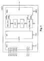
- FIG. 1 shows, in the form of a block diagram and in a particular embodiment of the invention, the timer / event counter device.
- the multifunctional timer / event counter device for example placed on a microcontroller chip, comprises a counter (CNT) controlled by a clock signal (CLK), a control register (REG_CTRL) comprising a binary number intended to to define a counter behavior (CNT) and a counter register (REG_CNT) containing a binary number representative of the state of the counter.
- This device also comprises a function module (MF), a first and a second selection module (MS1, MS2), and a delay means (D).
- the function control bits and the activation bits of the function module (MF) are, for example, sent to the function module (MF) by programming.
- the latter modifies the binary number contained in the control register (REG_CTRL) taking into account the signal synchronization so that the counter (CNT) resets on a rising edge of this synchronization signal.
- the latter modifies again the binary number contained in the control register (REG_CTRL) as a function of the state of the signal. synchronization so that the counter is triggered on a rising edge of the synchronization signal.
- the selection control bits are, for example, sent to the first selection module (MF) by programming.
- the second set of selection control bits is, for example, sent to the second selection module (MS2) by programming.
- the delay means (D) may, for example, consist of a set of flip-flops, known to those skilled in the art, driven by the clock signal (CLK) and active on a rising edge of the signal clock (CLK). If during a first clock cycle the binary number in the control register (REG_CTRL) is modified so that the counter (CNT) adopts a new behavior, for example triggering the counting, this new behavior will be taken into account by the counter (CNT) than at the next clock cycle.
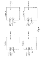
- FIG. 2 shows, in the form of a block diagram and in a particular application, two timer / event counter devices (TIMER_1, TIMER_2), the first device (TIMER_1) operating according to the first operating mode (SLAVE) and the second device (TIMER_2) operating according to the second operating mode (MASTER).
- TIMER_1, TIMER_2 two timer / event counter devices
- TIMER_1 operating according to the first operating mode
- TIMER_2 operating according to the second operating mode (MASTER).
- the synchronization output (TRGO) of the second device is connected to the first input (ITR_1) of the first selection module (MS1) of the first device (TIMER_1).
- This configuration makes it possible, for example, to trigger the counters of the two devices (TIMER_1, TIMER_2) during the same clock cycle.
- the modification, by direct programming, of the binary number contained in the second control register (REG_CTRL_2) makes it possible to trigger the first and second counter (CNT_1, CNT_2) during the same clock cycle.
- Figure 3 shows a timing diagram of the signals illustrating the operation of the devices in this particular application.
- CLK is the clock signal controlling the counters.
- RST_1 and RST_2 are respectively the reset signal of the first counter (CNT_1) and the second counter (CNT_2).
- EN_1 and EN_2 respectively represent the trigger signal of the first counter (CNT_1) and the second counter (CNT_2) sent respectively to the first control register (REG_CTRL_1) and the second control register (REG_CTRL_2).
- CNT1 and CNT2 represent respectively the value of the first counter (CNT_1) and the counter of the second device (TIMER_2).
- INCR - COUNTER - 1 and INCR_COUNTER_2 respectively represent the signal giving the order of start of counting at the first counter (CNT_1) and the signal giving the order of start of counting at the second counter (CNT_2), generated respectively by the first means of delay (D_1) and the second delay means (D_2).
- TRGO_2 represents the signal at the synchronization output of the second selection module (MS2) of the second device (TIMER_2).
- TRG represents the signal at the input of the first selection module (MS1) of the first device (TIMER_1).
- WRITE_CNT_1 represents the positioning signal of the value of the first counter (CNT_1).
- the second counter (CNT_2) is reset when RST_2 is high.
- the first counter (CNT_1) is reset when RST_1 is high.
- the first counter (CNT_1) is then initialized with the value 32487, or 7EE7 in hexadecimal notation, when WRITE_CNT_1 is high.
- EN_2 is set high, and is sent, via the second control register (REG_CTRL_2), to the second delay means (D_2) controlled by the same signal clock (CLK).
- EN_2 is sent to the synchronization output (TRGO) of the second device (TIMER 2).
- This synchronization output (TRGO) being connected to the first input (ITR_1) of the first selection module (MS1) of the first device (TIMER_1), EN_2 is sent to the input (TRG) of reception of a synchronization signal of the function module (MF) of the first device (TIMER_1).
- the binary number of the first control register (REG_CTRL_1) is then modified.
- the first delay means (D_1) driven by the same clock signal (CLK), receives the signal EN_2.
- the first delay means (D_1) and the second delay means (D_2) respectively generate the identical signals INCR_COUNTER_1 and INCR_COUNTER_2 at the signal EN_2.
- these signals INCR_COUNTER_1 and INCR_COUNTER_2 are respectively sent to the first counter (CNT_1) and second counter (CNT_2).
- the first and second counters are triggered during the same second clock cycle (C2).
- the synchronization of the two devices makes it possible, for example by positioning the initial values of the two counters and by configuring the comparison values in the registers, to construct two logic signals of the PWM type of different frequencies but of integer ratio, or two PWM logic signals out of phase with each other and with identical frequencies.
- each device can operate in the first mode of operation (SLAVE), then in the second mode of operation (MASTER).
- TRGO synchronization output
- MS1 first selection module
- MASTER second mode of operation
- each device can control other devices and be controlled by other devices. In this configuration it is thus possible to build very large frequency dividers.
Landscapes
- Engineering & Computer Science (AREA)
- Theoretical Computer Science (AREA)
- Physics & Mathematics (AREA)
- General Engineering & Computer Science (AREA)
- General Physics & Mathematics (AREA)
- Synchronisation In Digital Transmission Systems (AREA)
- Electronic Switches (AREA)
Applications Claiming Priority (1)
| Application Number | Priority Date | Filing Date | Title |
|---|---|---|---|
| FR0512818A FR2895101A1 (fr) | 2005-12-16 | 2005-12-16 | Dispositif multifonctionnel temporisateur/compteur d'evenements et procede de mise en oeuvre d'un tel dispositif. |
Publications (1)
| Publication Number | Publication Date |
|---|---|
| EP1798628A1 true EP1798628A1 (de) | 2007-06-20 |
Family
ID=36637039
Family Applications (1)
| Application Number | Title | Priority Date | Filing Date |
|---|---|---|---|
| EP06291700A Withdrawn EP1798628A1 (de) | 2005-12-16 | 2006-10-31 | Zeitgeber/Zähler und dazugehöriges Verfahren |
Country Status (3)
| Country | Link |
|---|---|
| US (1) | US7725758B2 (de) |
| EP (1) | EP1798628A1 (de) |
| FR (1) | FR2895101A1 (de) |
Families Citing this family (3)
| Publication number | Priority date | Publication date | Assignee | Title |
|---|---|---|---|---|
| KR20120012119A (ko) * | 2010-07-30 | 2012-02-09 | 주식회사 하이닉스반도체 | 레이턴시 제어 회로 및 그의 동작 방법 |
| US9715387B2 (en) * | 2015-06-05 | 2017-07-25 | Renesas Electronics America Inc. | Configurable event selection for microcontroller timer/counter unit control |
| KR102522154B1 (ko) * | 2016-03-15 | 2023-04-17 | 에스케이하이닉스 주식회사 | 반도체 메모리 장치의 컨트롤러 및 이의 동작 방법 |
Citations (3)
| Publication number | Priority date | Publication date | Assignee | Title |
|---|---|---|---|---|
| GB1323166A (en) * | 1969-09-19 | 1973-07-11 | Burroughs Corp | Digital processing systems |
| US5724399A (en) * | 1995-09-06 | 1998-03-03 | Mitsubishi Electric Semiconductor Software Co., Ltd. | Timer device |
| US5935236A (en) * | 1997-08-08 | 1999-08-10 | Mitsubishi Denki Kabushiki Kaisha | Microcomputer capable of outputting pulses |
Family Cites Families (6)
| Publication number | Priority date | Publication date | Assignee | Title |
|---|---|---|---|---|
| USRE29086E (en) * | 1963-03-20 | 1976-12-21 | P. R. Mallory & Co., Inc. | Adjustable interval time switch device |
| US4720821A (en) * | 1986-02-05 | 1988-01-19 | Ke Jenn Yuh | Timer device |
| US5042005A (en) * | 1988-08-19 | 1991-08-20 | Motorola, Inc. | Timer channel with match recognition features |
| KR0133827B1 (ko) * | 1993-12-31 | 1998-04-23 | 조태현 | 스위치에 의해 제어되는 타이머장치 |
| IT235873Y1 (it) * | 1995-06-01 | 2000-07-18 | Finder Spa | Temporizzatore multifunzionale |
| JP3082721B2 (ja) * | 1997-09-19 | 2000-08-28 | 日本電気株式会社 | タイマ装置 |
-
2005
- 2005-12-16 FR FR0512818A patent/FR2895101A1/fr not_active Withdrawn
-
2006
- 2006-10-31 EP EP06291700A patent/EP1798628A1/de not_active Withdrawn
- 2006-12-18 US US11/641,607 patent/US7725758B2/en active Active
Patent Citations (3)
| Publication number | Priority date | Publication date | Assignee | Title |
|---|---|---|---|---|
| GB1323166A (en) * | 1969-09-19 | 1973-07-11 | Burroughs Corp | Digital processing systems |
| US5724399A (en) * | 1995-09-06 | 1998-03-03 | Mitsubishi Electric Semiconductor Software Co., Ltd. | Timer device |
| US5935236A (en) * | 1997-08-08 | 1999-08-10 | Mitsubishi Denki Kabushiki Kaisha | Microcomputer capable of outputting pulses |
Also Published As
| Publication number | Publication date |
|---|---|
| US7725758B2 (en) | 2010-05-25 |
| US20070164796A1 (en) | 2007-07-19 |
| FR2895101A1 (fr) | 2007-06-22 |
Similar Documents
| Publication | Publication Date | Title |
|---|---|---|
| FR2709624A1 (fr) | Synthétiseur de fréquence. | |
| JP2014099925A (ja) | 分数クロック信号を生成するための技術 | |
| FR2922697A1 (fr) | Synthetiseur de frequence numerique | |
| EP3242398A1 (de) | Generator von schwingungszahlen | |
| EP0881772B1 (de) | Frequenzteilungsvorrichtung, bestehend aus einem Vorzähler gefolgt von einem programmierbaren Zähler und Anwendung in einem Frequenzsynthetisierer | |
| FR2473814A1 (fr) | Circuit mos dynamique ne dependant pas d'un rapport de resistances destine a constituer des circuits logiques divers | |
| FR2666707A1 (fr) | Dispositif de division de frequence programmable. | |
| EP1798628A1 (de) | Zeitgeber/Zähler und dazugehöriges Verfahren | |
| FR2824970A1 (fr) | Selecteur de phase fonctionnant a grande vitesse | |
| FR2783649A1 (fr) | Circuit de filtrage d'un signal d'horloge | |
| FR2522826A1 (fr) | Dispositif de generation numerique d'un signal module en frequence et dispositif radiofrequence comprenant un tel dispositif numerique | |
| EP0475862A1 (de) | Schneller Zähler/Teiler und dessen Verwendung in einem Zähler mit Impulsunterdrückung | |
| EP3376670A1 (de) | Konfigurierbare verzögerungsleitung | |
| CA2040650C (fr) | Circuit de multiplexage de signaux d'horloge | |
| EP3242397A1 (de) | Multiplexerstruktur | |
| EP0616279B1 (de) | Taktgeber mit auswählbarer Quelle und fehlimpulsfreier Rücksetzfunktion | |
| FR2601532A1 (fr) | Dispositif de commande ou de controle d'une generateur de sequence lineairement recurrente | |
| EP0105837B1 (de) | Nichtlineare Zählschaltung | |
| EP1299951B1 (de) | Verfahren und anordnung zur frequenzsynthese mit einer phasenregelschleife | |
| FR2631470A1 (fr) | Unite de controle d'un circuit integre de traitement de donnees | |
| EP0658838B1 (de) | Frequenzsynthetisierer | |
| EP2057533A1 (de) | Generator für pseudoperiodische logische signale | |
| FR2770006A1 (fr) | Circuit de remise a l'etat initial synchrone ou asynchrone | |
| EP1445865A1 (de) | Frequenzteiler mit Trichterstruktur | |
| EP0463917B1 (de) | Digitale Anordnung zur bedingten Initialisierung |
Legal Events
| Date | Code | Title | Description |
|---|---|---|---|
| PUAI | Public reference made under article 153(3) epc to a published international application that has entered the european phase |
Free format text: ORIGINAL CODE: 0009012 |
|
| AK | Designated contracting states |
Kind code of ref document: A1 Designated state(s): AT BE BG CH CY CZ DE DK EE ES FI FR GB GR HU IE IS IT LI LT LU LV MC NL PL PT RO SE SI SK TR |
|
| AX | Request for extension of the european patent |
Extension state: AL BA HR MK YU |
|
| 17P | Request for examination filed |
Effective date: 20071129 |
|
| 17Q | First examination report despatched |
Effective date: 20080111 |
|
| AKX | Designation fees paid |
Designated state(s): DE FR GB IT |
|
| STAA | Information on the status of an ep patent application or granted ep patent |
Free format text: STATUS: THE APPLICATION IS DEEMED TO BE WITHDRAWN |
|
| 18D | Application deemed to be withdrawn |
Effective date: 20081018 |