EP1798671A2 - Méthode de fabrication d'un support de données de la forme d'une carte - Google Patents
Méthode de fabrication d'un support de données de la forme d'une carte Download PDFInfo
- Publication number
- EP1798671A2 EP1798671A2 EP06025597A EP06025597A EP1798671A2 EP 1798671 A2 EP1798671 A2 EP 1798671A2 EP 06025597 A EP06025597 A EP 06025597A EP 06025597 A EP06025597 A EP 06025597A EP 1798671 A2 EP1798671 A2 EP 1798671A2
- Authority
- EP
- European Patent Office
- Prior art keywords
- data carrier
- card
- chip card
- card body
- outer contour
- Prior art date
- Legal status (The legal status is an assumption and is not a legal conclusion. Google has not performed a legal analysis and makes no representation as to the accuracy of the status listed.)
- Granted
Links
Images

Classifications
-
- G—PHYSICS
- G06—COMPUTING OR CALCULATING; COUNTING
- G06K—GRAPHICAL DATA READING; PRESENTATION OF DATA; RECORD CARRIERS; HANDLING RECORD CARRIERS
- G06K19/00—Record carriers for use with machines and with at least a part designed to carry digital markings
- G06K19/06—Record carriers for use with machines and with at least a part designed to carry digital markings characterised by the kind of the digital marking, e.g. shape, nature, code
- G06K19/067—Record carriers with conductive marks, printed circuits or semiconductor circuit elements, e.g. credit or identity cards also with resonating or responding marks without active components
- G06K19/07—Record carriers with conductive marks, printed circuits or semiconductor circuit elements, e.g. credit or identity cards also with resonating or responding marks without active components with integrated circuit chips
- G06K19/077—Constructional details, e.g. mounting of circuits in the carrier
-
- B—PERFORMING OPERATIONS; TRANSPORTING
- B26—HAND CUTTING TOOLS; CUTTING; SEVERING
- B26D—CUTTING; DETAILS COMMON TO MACHINES FOR PERFORATING, PUNCHING, CUTTING-OUT, STAMPING-OUT OR SEVERING
- B26D3/00—Cutting work characterised by the nature of the cut made; Apparatus therefor
- B26D3/08—Making a superficial cut in the surface of the work without removal of material, e.g. scoring, incising
-
- B—PERFORMING OPERATIONS; TRANSPORTING
- B26—HAND CUTTING TOOLS; CUTTING; SEVERING
- B26D—CUTTING; DETAILS COMMON TO MACHINES FOR PERFORATING, PUNCHING, CUTTING-OUT, STAMPING-OUT OR SEVERING
- B26D3/00—Cutting work characterised by the nature of the cut made; Apparatus therefor
- B26D3/08—Making a superficial cut in the surface of the work without removal of material, e.g. scoring, incising
- B26D3/085—On sheet material
-
- B—PERFORMING OPERATIONS; TRANSPORTING
- B26—HAND CUTTING TOOLS; CUTTING; SEVERING
- B26F—PERFORATING; PUNCHING; CUTTING-OUT; STAMPING-OUT; SEVERING BY MEANS OTHER THAN CUTTING
- B26F1/00—Perforating; Punching; Cutting-out; Stamping-out; Apparatus therefor
- B26F1/38—Cutting-out; Stamping-out
- B26F1/44—Cutters therefor; Dies therefor
-
- G—PHYSICS
- G06—COMPUTING OR CALCULATING; COUNTING
- G06K—GRAPHICAL DATA READING; PRESENTATION OF DATA; RECORD CARRIERS; HANDLING RECORD CARRIERS
- G06K19/00—Record carriers for use with machines and with at least a part designed to carry digital markings
- G06K19/06—Record carriers for use with machines and with at least a part designed to carry digital markings characterised by the kind of the digital marking, e.g. shape, nature, code
- G06K19/067—Record carriers with conductive marks, printed circuits or semiconductor circuit elements, e.g. credit or identity cards also with resonating or responding marks without active components
- G06K19/07—Record carriers with conductive marks, printed circuits or semiconductor circuit elements, e.g. credit or identity cards also with resonating or responding marks without active components with integrated circuit chips
- G06K19/077—Constructional details, e.g. mounting of circuits in the carrier
- G06K19/07737—Constructional details, e.g. mounting of circuits in the carrier the record carrier consisting of two or more mechanically separable parts
- G06K19/07739—Constructional details, e.g. mounting of circuits in the carrier the record carrier consisting of two or more mechanically separable parts comprising a first part capable of functioning as a record carrier on its own and a second part being only functional as a form factor changing part, e.g. SIM cards type ID 0001, removably attached to a regular smart card form factor
Definitions
- the invention relates to a method for producing a card-shaped data carrier. Furthermore, the invention relates to a semifinished product for a card-shaped data carrier and a card-shaped data carrier.
- the data carrier is, in particular, a chip card in the format ID-000 of the ISO-7810 standard, which is referred to below as a mini chip card.
- Mini chip cards are used in particular in mobile devices. Depending on the size of the mobile device, it is also possible to use conventional chip cards in the format ID-1 of the ISO-7810 standard, which are referred to below as standard chip cards.
- the procedure is such that the mini chip card is produced as an integral part of a standard chip card and is separated from the card body of the standard chip card only immediately prior to the first use.
- the mini chip card is also referred to as a "plug-in".
- the standard chip card is first produced in accordance with a customary production method and provided with punches along the contours of the mini chip card so that the mini chip card remains connected to the standard chip card only via narrow webs. Thereafter, the integrated circuit is tested and initialized. Finally, there follows the electrical and optical personalization of the mini chip card.
- Such a manufacturing method is for example in the DE 40 07 221 A1 disclosed.
- the method described there has the special feature that a positioning of the standard chip card for precise punching of the contour of the mini chip card is carried out by means of a test head.
- mini chip cards As an alternative to producing the mini chip card by punching it out of a chip card of a larger format, it is also possible to produce the mini chip card directly in its final format by means of an injection molding process. In contrast to punching, in which sharp 90 ° edges are produced in the punching area, mini chip cards with rounded edges can be produced with the injection molding technique. Rounded edges are required, for example, when the mini chip cards are to be used as multimedia cards, since the relevant specification prescribes a rounding of the edges. In the production of mini chip cards by injection molding, however, the possibilities of designing the card surface are limited.
- the invention is therefore based on the object to produce card-shaped disk with rounded edges in the best possible way.
- a card body is produced in a format larger than the format of the data carrier such that the card body has the data carrier as an integral part.
- the card body is partially severed along a provided outer contour of the data carrier and / or at least partially weakened.
- the inventive method is characterized in that the card body along the outer contour of the data carrier is at least partially deformed and thereby the outer contour of the data carrier is at least partially formed as a rounded edge.
- the method according to the invention has the advantage that small-sized data carriers of high quality can be produced which have rounded edges. It is particularly advantageous that can be used in part to process steps that are already used in the production of larger-sized disk used. This makes it possible, for example, to produce small-sized data carriers that have a design print.
- the card body is deformed in the region of the data carrier in such a way that a depression is formed.
- the recess can serve, for example, as a grip groove, which facilitates the handling of the data carrier.
- the deformation of the card body may be performed during the severing and / or weakening of the card body. As a result, separate work steps for the deformation can be omitted, so that an efficient production is possible.
- the deformation of the card body is performed after the severing and / or weakening of the card body.
- the deformation of the card body is performed by means of at least one embossing operation. Embossing operations can be performed quickly and inexpensively. In this case, it is also possible in particular for the deformation of the card body to be carried out with the supply of heat. This has the advantage that the deformation can be carried out with a lower force than in the cold state.
- the card body can be produced in particular by lamination. In this way, both a high quality and a sophisticated appearance of the disk can be achieved.
- the invention further relates to a flat piece-like semifinished product which has a card-shaped data carrier with an integrated circuit for storing and / or processing data as an integral component and partially severed along an outer contour of the data carrier and / or is at least partially weakened.
- the semifinished product according to the invention is characterized in that the outer contour of the data carrier is at least partially formed as a rounded edge.
- a user can remove the data carrier without technical aids, which, despite being cut out, is not sharp-edged but has rounded edges.
- the semifinished product is preferably designed as a chip card with standardized dimensions.
- the chip card may in particular have the format ID-1 according to the standard ISO-7810.
- For smart cards of this format sophisticated production processes are available.
- smart cards of this format can be handled very well.
- the invention relates to a laminated card-shaped data carrier with an integrated circuit for storing and / or processing data.
- the data carrier according to the invention has an outer contour, which is at least partially formed as a rounded edge.
- a rounded edge is formed on each of the two major surfaces of the data carrier.
- the edge may in particular have an edge radius between 0.05 mm and 0.2 mm.
- the data carrier can have an increased material density in an area adjoining the rounded edge. Furthermore, at least one main surface of the data carrier may have a depression.
- the data carrier is designed as a chip card with standardized dimensions. In this case, the chip card in particular the format ID-000 according to the standard ISO -7810. In a preferred embodiment, the data carrier is designed as a multimedia card.
- Fig. 1 shows an embodiment of a mini chip card 1 according to the invention, which is formed as part of a chip card of a larger format, in supervision.
- the large-sized chip card will be referred to as a standard chip card 2 for the purpose of discrimination in the following and may have, for example, the ID-1 format according to the ISO 7810 standard.
- the mini chip card 1 may, for example, have the format ID-000 of the same standard.
- the standard chip card 2 has a card body 3 containing the mini chip card 1 as an integral part.
- the mini chip card 1 has an integrated circuit 4 and a contact surface 5 for the contacting contacting of the integrated circuit 4.
- a grip groove 6 is formed on the surface of the mini chip card 1 in order to facilitate the handling of the mini chip card 1.
- the mini chip card 1 is limited by an outer circumferential edge 7 in their lateral dimensions. Over several narrow webs 8, the mini chip card 1 is connected to the card body 3 of the standard chip card 2. Outside the webs 8, the mini chip card 1 is separated from the card body 3 of the standard chip card 2 by free punches 9.
- the webs 8 are dimensioned so that the mini chip card 1 can be separated out by a user without additional aids from the card body 3 of the standard chip card 2.
- the mini chip card 1 may also be connected in other ways with the card body 3 of the standard chip card 2 that a separation of the mini chip card 1 without tools is possible.
- FIGS. 2, 3 and 4 section lines AA, BB and CC are shown.
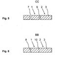
- the associated sectional views are shown in FIGS. 2, 3 and 4. These sectional representations are drawn for reasons of clarity strongly unansstäsch. In addition, only the outer contour of the cut surface is shown. The same applies to the sectional views of FIGS. 5 and 6.
- FIG. 2 shows the standard chip card 2 shown in FIG. 1, including the mini chip card 1 in a sectional representation.
- the section is guided along the section line AA drawn in FIG. 1, which extends parallel to the longitudinal side of the mini chip card 1 and extends centrally through the mini chip card 1.
- both one of the webs 8 and one of the free breaks 9 is detected by the section.
- the card body 3 in the region of the web 8 has a reduced thickness.
- the sectional area in the region of the web 8 is profiled so that the edge 7 is rounded.
- the edge radius preferably has a value between about 0.05 mm and 0.2 mm, in particular a value of about 0.1 mm. Due to the manufacturing process, a rounding can likewise be formed in the adjacent area of the standard chip card 2.
- the edge 7 of the mini chip card 1 is likewise rounded off, wherein the edge radius in turn preferably has values in the interval mentioned having.
- the edges 7 of both main surfaces of the mini chip card 1 are rounded off.
- the mini chip card 1 has a rounded edge 7 both on its front side and on its rear side.
- the mini chip card 1 Since the mini chip card 1 is connected only via the webs 8 with the standard chip card 2 and also the thickness of the card body 3 is reduced in the region of the webs 8, the mini chip card 1 can be separated from the standard chip card 2 by a user without technical aids. After separation, preferably both main surfaces of the mini chip card 1 each have a peripheral edge 7, which is rounded over its entire length.
- FIG. 3 shows the standard chip card 2 shown in FIG. 1, including the mini chip card 1 in a further sectional view.
- the section is taken along the drawn in Fig. 1 section line BB, which crosses the mini chip card 1 in the region of two webs 8.
- the card body 3 also has a reduced thickness in the region of the webs 8 shown in FIG. 3, wherein in turn the outer contour of the mini chip card 1 is formed by a rounded edge 7.
- the webs 8 shown in Fig. 3 are formed analogous to the web 8 shown in Fig. 2.
- FIG. 4 shows the standard chip card 2 shown in FIG. 1, including the mini chip card 1 in a different sectional view again.
- the section is taken along the section line CC drawn in FIG. 1, which crosses the mini chip card 1 in the region of two free positions 9.
- the edge 7 of the mini chip card 1 in the area of both free punches 9 is rounded off.
- the standard chip card 2 is produced according to a method known per se, preferably by laminating a plurality of plastic films. Preferably, at least one of the plastic films is provided with a print before the lamination.
- the card body 3 is formed and equipped with the integrated circuit 4 and the contact surface 5 for contacting the integrated circuit 4 contacting.
- FIG. 5 shows the standard chip card 2 including the mini chip card 1 after the punching operation in a representation corresponding to FIG.
- the edges 7 of the mini chip card 1 in FIG. 5 are not rounded off in the area of the free punches 9, but have a sharp-edged design.
- the webs 8 are weakened by a notching operation. This is shown in FIG.
- FIG. 6 shows the standard chip card 2 including the mini chip card 1 after the notching operation in a representation corresponding to FIG.
- the webs 8 are provided, starting from two main surfaces, each with a notch 10.
- the notches 10 are formed on both major surfaces congruent to each other and extend is so deep in the card body 3, that a non-severed core region is maintained, which preferably has a thickness of about 200 microns to 300 microns, in particular a thickness of about 250 microns.
- the edges 7 of the mini chip card 1 are rounded by a stamping operation.
- an embossing punch is pressed against the card body 3 and thereby the card material is deformed so that the edges 7 are each rounded.
- the embossing operation can be carried out simultaneously on both main surfaces of the mini chip card 1.
- the embossing operation can be performed either in the cold state or supported by heat.
- material of the card body 3 can be displaced into an area adjacent to the edge 7.
- material compaction may occur within this range.
- the grip groove 6 of the mini chip card 1 can be formed and it can be made if necessary further imprints.
- the standard chip card 2 with integrated mini chip card 1 shown in FIGS. 1 to 4 results.
- the embossing operation may also be performed before the punching and the scoring operation. It is particularly advantageous if the embossing operation is carried out together with the punching operation.
Landscapes
- Engineering & Computer Science (AREA)
- Life Sciences & Earth Sciences (AREA)
- Forests & Forestry (AREA)
- Mechanical Engineering (AREA)
- Computer Hardware Design (AREA)
- Microelectronics & Electronic Packaging (AREA)
- Physics & Mathematics (AREA)
- General Physics & Mathematics (AREA)
- Theoretical Computer Science (AREA)
- Credit Cards Or The Like (AREA)
- Manufacturing Optical Record Carriers (AREA)
Applications Claiming Priority (1)
| Application Number | Priority Date | Filing Date | Title |
|---|---|---|---|
| DE102005059964A DE102005059964A1 (de) | 2005-12-15 | 2005-12-15 | Verfahren zum Herstellen eines kartenförmigen Datenträgers |
Publications (3)
| Publication Number | Publication Date |
|---|---|
| EP1798671A2 true EP1798671A2 (fr) | 2007-06-20 |
| EP1798671A3 EP1798671A3 (fr) | 2008-04-23 |
| EP1798671B1 EP1798671B1 (fr) | 2010-06-30 |
Family
ID=37813806
Family Applications (1)
| Application Number | Title | Priority Date | Filing Date |
|---|---|---|---|
| EP06025597A Not-in-force EP1798671B1 (fr) | 2005-12-15 | 2006-12-11 | Méthode de fabrication d'un support de données de la forme d'une carte |
Country Status (3)
| Country | Link |
|---|---|
| EP (1) | EP1798671B1 (fr) |
| AT (1) | ATE472781T1 (fr) |
| DE (2) | DE102005059964A1 (fr) |
Cited By (2)
| Publication number | Priority date | Publication date | Assignee | Title |
|---|---|---|---|---|
| GB2463236A (en) * | 2008-09-03 | 2010-03-10 | Beautiful Card Corp | SIM card forming structure |
| EP2664424A1 (fr) * | 2012-05-14 | 2013-11-20 | Oberthur Technologies | Outil de poinçonnage |
Families Citing this family (1)
| Publication number | Priority date | Publication date | Assignee | Title |
|---|---|---|---|---|
| DE102023111397A1 (de) * | 2023-05-03 | 2024-11-07 | Giesecke+Devrient ePayments GmbH | Verfahren zum Herstellen eines Kartenelements |
Citations (4)
| Publication number | Priority date | Publication date | Assignee | Title |
|---|---|---|---|---|
| DE4007221A1 (de) | 1990-03-07 | 1991-09-12 | Gao Ges Automation Org | Pruefkopf fuer kontaktflaechen von wertkarten mit eingelagertem halbleiterchip |
| DE19703122C1 (de) | 1997-01-29 | 1998-05-20 | Orga Kartensysteme Gmbh | Verfahren zur Herstellung von Datenträgern |
| WO2001088845A1 (fr) | 2000-05-15 | 2001-11-22 | Giesecke & Devrient Gmbh | Dispositif de poinconnage de matieres plastiques |
| WO2003027946A1 (fr) | 2001-09-24 | 2003-04-03 | Gemplus | Cle electronique destinee a etre connectee a un port d'un dispositif de telecommunication |
Family Cites Families (4)
| Publication number | Priority date | Publication date | Assignee | Title |
|---|---|---|---|---|
| FR2773900B1 (fr) * | 1998-01-22 | 2000-02-18 | Gemplus Card Int | Carte a circuit(s) integre(s) a contact, comportant une minicarte detachable |
| EP1018702B1 (fr) * | 1999-01-04 | 2010-04-14 | X-ident technology GmbH | Unités des matériaux composites avec transpondeur |
| FR2794264B1 (fr) * | 1999-05-27 | 2001-11-02 | Gemplus Card Int | Adaptateur pour dispositif electronique portable a circuit integre, de type carte a puce, d'un format reduit par rapport au format standard d'une mini-carte |
| DE19935174A1 (de) * | 1999-07-28 | 2001-02-08 | Friedrich Winter | Verfahren zum Herstellen einer Plastikkarte, Trägermaterial sowie Produktkombination aus Trägermaterial und Computerprogrammprodukt |
-
2005
- 2005-12-15 DE DE102005059964A patent/DE102005059964A1/de not_active Withdrawn
-
2006
- 2006-12-11 EP EP06025597A patent/EP1798671B1/fr not_active Not-in-force
- 2006-12-11 AT AT06025597T patent/ATE472781T1/de active
- 2006-12-11 DE DE502006007315T patent/DE502006007315D1/de active Active
Patent Citations (4)
| Publication number | Priority date | Publication date | Assignee | Title |
|---|---|---|---|---|
| DE4007221A1 (de) | 1990-03-07 | 1991-09-12 | Gao Ges Automation Org | Pruefkopf fuer kontaktflaechen von wertkarten mit eingelagertem halbleiterchip |
| DE19703122C1 (de) | 1997-01-29 | 1998-05-20 | Orga Kartensysteme Gmbh | Verfahren zur Herstellung von Datenträgern |
| WO2001088845A1 (fr) | 2000-05-15 | 2001-11-22 | Giesecke & Devrient Gmbh | Dispositif de poinconnage de matieres plastiques |
| WO2003027946A1 (fr) | 2001-09-24 | 2003-04-03 | Gemplus | Cle electronique destinee a etre connectee a un port d'un dispositif de telecommunication |
Cited By (2)
| Publication number | Priority date | Publication date | Assignee | Title |
|---|---|---|---|---|
| GB2463236A (en) * | 2008-09-03 | 2010-03-10 | Beautiful Card Corp | SIM card forming structure |
| EP2664424A1 (fr) * | 2012-05-14 | 2013-11-20 | Oberthur Technologies | Outil de poinçonnage |
Also Published As
| Publication number | Publication date |
|---|---|
| EP1798671A3 (fr) | 2008-04-23 |
| DE502006007315D1 (de) | 2010-08-12 |
| DE102005059964A1 (de) | 2007-06-28 |
| ATE472781T1 (de) | 2010-07-15 |
| EP1798671B1 (fr) | 2010-06-30 |
Similar Documents
| Publication | Publication Date | Title |
|---|---|---|
| EP0823099B1 (fr) | Carte en plastique munie d'une carte amovible a puce miniature | |
| DE10338444A1 (de) | Transponderinlay für ein Dokument zur Personenidentifikation sowie Verfahren zu dessen Herstellung | |
| EP2435958B1 (fr) | Procédé de fabrication de supports de données portables | |
| EP1889696A1 (fr) | Appareil pour le poinçonage et méthode utilisant un tel appareil | |
| DE4122049A1 (de) | Verfahren zum einbau eines traegerelements | |
| EP1285405B1 (fr) | Dispositif de poinconnage de matieres plastiques | |
| EP2936397B1 (fr) | Procédé de fabrication d'une incrustation et incrustation pour un ensemble de feuilles pour un document de valeur ou de sécurité | |
| DE102009034437A1 (de) | Vorrichtung und Verfahren zur Ausbildung einer Kontur in einem Kartenkörper für einen tragbaren Datenträger, insbesondere für eine Chipkarte | |
| DE102012001776A1 (de) | Chipkarte mit heraustrennbarer Miniaturchipkarte | |
| EP1798671B1 (fr) | Méthode de fabrication d'un support de données de la forme d'une carte | |
| EP1449415B1 (fr) | Procede et dispositif de metallisation de substrats et plaquettes | |
| DE102021003336A1 (de) | Verfahren zum Herstellen eines Chipkartenkörpers | |
| EP2059891B1 (fr) | Procédé de fabrication d'un support de données en forme de carte | |
| EP3183694B1 (fr) | Support de données pourvu d'un élément | |
| EP1828966B1 (fr) | Carte a puce comportant un module sim integre | |
| EP2690584A1 (fr) | Procédé de fabrication dýun module de puce | |
| DE10234751B4 (de) | Verfahren zur Herstellung einer spritzgegossenen Chipkarte und nach dem Verfahren hergestellte Chipkarte | |
| WO2020169576A1 (fr) | Procédé de fabrication d'un document de valeur ou de sécurité ainsi que document de sécurité pourvu d'un hologramme de sécurité | |
| EP3120301B1 (fr) | Procédé de fabrication d'un module à puce électronique | |
| DE102020007084A1 (de) | Verfahren zum Herstellen eines mehrschichtigen Kartenkörpers | |
| DE102023111397A1 (de) | Verfahren zum Herstellen eines Kartenelements | |
| DE102013104824A1 (de) | Kontaktpad-Trägerstreifen und Verfahren zum Herstellen desselben | |
| EP4621641A1 (fr) | Fabrication d'un corps support pour un support de données portable | |
| EP4523923A1 (fr) | Support de données en forme de carte et procédé de fabrication d'un support de données en forme de carte | |
| EP3081057B1 (fr) | Procédé permettant de produire une bande modulaire |
Legal Events
| Date | Code | Title | Description |
|---|---|---|---|
| PUAI | Public reference made under article 153(3) epc to a published international application that has entered the european phase |
Free format text: ORIGINAL CODE: 0009012 |
|
| AK | Designated contracting states |
Kind code of ref document: A2 Designated state(s): AT BE BG CH CY CZ DE DK EE ES FI FR GB GR HU IE IS IT LI LT LU LV MC NL PL PT RO SE SI SK TR |
|
| AX | Request for extension of the european patent |
Extension state: AL BA HR MK YU |
|
| PUAL | Search report despatched |
Free format text: ORIGINAL CODE: 0009013 |
|
| AK | Designated contracting states |
Kind code of ref document: A3 Designated state(s): AT BE BG CH CY CZ DE DK EE ES FI FR GB GR HU IE IS IT LI LT LU LV MC NL PL PT RO SE SI SK TR |
|
| AX | Request for extension of the european patent |
Extension state: AL BA HR MK RS |
|
| 17P | Request for examination filed |
Effective date: 20081023 |
|
| 17Q | First examination report despatched |
Effective date: 20081124 |
|
| AKX | Designation fees paid |
Designated state(s): AT BE BG CH CY CZ DE DK EE ES FI FR GB GR HU IE IS IT LI LT LU LV MC NL PL PT RO SE SI SK TR |
|
| GRAP | Despatch of communication of intention to grant a patent |
Free format text: ORIGINAL CODE: EPIDOSNIGR1 |
|
| GRAS | Grant fee paid |
Free format text: ORIGINAL CODE: EPIDOSNIGR3 |
|
| GRAA | (expected) grant |
Free format text: ORIGINAL CODE: 0009210 |
|
| AK | Designated contracting states |
Kind code of ref document: B1 Designated state(s): AT BE BG CH CY CZ DE DK EE ES FI FR GB GR HU IE IS IT LI LT LU LV MC NL PL PT RO SE SI SK TR |
|
| REG | Reference to a national code |
Ref country code: CH Ref legal event code: EP Ref country code: GB Ref legal event code: FG4D Free format text: NOT ENGLISH |
|
| REG | Reference to a national code |
Ref country code: IE Ref legal event code: FG4D Free format text: LANGUAGE OF EP DOCUMENT: GERMAN |
|
| REF | Corresponds to: |
Ref document number: 502006007315 Country of ref document: DE Date of ref document: 20100812 Kind code of ref document: P |
|
| REG | Reference to a national code |
Ref country code: NL Ref legal event code: VDEP Effective date: 20100630 |
|
| PG25 | Lapsed in a contracting state [announced via postgrant information from national office to epo] |
Ref country code: LT Free format text: LAPSE BECAUSE OF FAILURE TO SUBMIT A TRANSLATION OF THE DESCRIPTION OR TO PAY THE FEE WITHIN THE PRESCRIBED TIME-LIMIT Effective date: 20100630 Ref country code: SE Free format text: LAPSE BECAUSE OF FAILURE TO SUBMIT A TRANSLATION OF THE DESCRIPTION OR TO PAY THE FEE WITHIN THE PRESCRIBED TIME-LIMIT Effective date: 20100630 |
|
| LTIE | Lt: invalidation of european patent or patent extension |
Effective date: 20100630 |
|
| PG25 | Lapsed in a contracting state [announced via postgrant information from national office to epo] |
Ref country code: LV Free format text: LAPSE BECAUSE OF FAILURE TO SUBMIT A TRANSLATION OF THE DESCRIPTION OR TO PAY THE FEE WITHIN THE PRESCRIBED TIME-LIMIT Effective date: 20100630 Ref country code: FI Free format text: LAPSE BECAUSE OF FAILURE TO SUBMIT A TRANSLATION OF THE DESCRIPTION OR TO PAY THE FEE WITHIN THE PRESCRIBED TIME-LIMIT Effective date: 20100630 Ref country code: SI Free format text: LAPSE BECAUSE OF FAILURE TO SUBMIT A TRANSLATION OF THE DESCRIPTION OR TO PAY THE FEE WITHIN THE PRESCRIBED TIME-LIMIT Effective date: 20100630 |
|
| PG25 | Lapsed in a contracting state [announced via postgrant information from national office to epo] |
Ref country code: GR Free format text: LAPSE BECAUSE OF FAILURE TO SUBMIT A TRANSLATION OF THE DESCRIPTION OR TO PAY THE FEE WITHIN THE PRESCRIBED TIME-LIMIT Effective date: 20101001 Ref country code: PL Free format text: LAPSE BECAUSE OF FAILURE TO SUBMIT A TRANSLATION OF THE DESCRIPTION OR TO PAY THE FEE WITHIN THE PRESCRIBED TIME-LIMIT Effective date: 20100630 |
|
| PG25 | Lapsed in a contracting state [announced via postgrant information from national office to epo] |
Ref country code: NL Free format text: LAPSE BECAUSE OF FAILURE TO SUBMIT A TRANSLATION OF THE DESCRIPTION OR TO PAY THE FEE WITHIN THE PRESCRIBED TIME-LIMIT Effective date: 20100630 Ref country code: EE Free format text: LAPSE BECAUSE OF FAILURE TO SUBMIT A TRANSLATION OF THE DESCRIPTION OR TO PAY THE FEE WITHIN THE PRESCRIBED TIME-LIMIT Effective date: 20100630 |
|
| REG | Reference to a national code |
Ref country code: IE Ref legal event code: FD4D |
|
| PG25 | Lapsed in a contracting state [announced via postgrant information from national office to epo] |
Ref country code: CY Free format text: LAPSE BECAUSE OF FAILURE TO SUBMIT A TRANSLATION OF THE DESCRIPTION OR TO PAY THE FEE WITHIN THE PRESCRIBED TIME-LIMIT Effective date: 20100630 Ref country code: SK Free format text: LAPSE BECAUSE OF FAILURE TO SUBMIT A TRANSLATION OF THE DESCRIPTION OR TO PAY THE FEE WITHIN THE PRESCRIBED TIME-LIMIT Effective date: 20100630 Ref country code: RO Free format text: LAPSE BECAUSE OF FAILURE TO SUBMIT A TRANSLATION OF THE DESCRIPTION OR TO PAY THE FEE WITHIN THE PRESCRIBED TIME-LIMIT Effective date: 20100630 Ref country code: PT Free format text: LAPSE BECAUSE OF FAILURE TO SUBMIT A TRANSLATION OF THE DESCRIPTION OR TO PAY THE FEE WITHIN THE PRESCRIBED TIME-LIMIT Effective date: 20101102 Ref country code: IS Free format text: LAPSE BECAUSE OF FAILURE TO SUBMIT A TRANSLATION OF THE DESCRIPTION OR TO PAY THE FEE WITHIN THE PRESCRIBED TIME-LIMIT Effective date: 20101030 Ref country code: CZ Free format text: LAPSE BECAUSE OF FAILURE TO SUBMIT A TRANSLATION OF THE DESCRIPTION OR TO PAY THE FEE WITHIN THE PRESCRIBED TIME-LIMIT Effective date: 20100630 |
|
| PG25 | Lapsed in a contracting state [announced via postgrant information from national office to epo] |
Ref country code: IT Free format text: LAPSE BECAUSE OF FAILURE TO SUBMIT A TRANSLATION OF THE DESCRIPTION OR TO PAY THE FEE WITHIN THE PRESCRIBED TIME-LIMIT Effective date: 20100630 |
|
| PG25 | Lapsed in a contracting state [announced via postgrant information from national office to epo] |
Ref country code: IE Free format text: LAPSE BECAUSE OF FAILURE TO SUBMIT A TRANSLATION OF THE DESCRIPTION OR TO PAY THE FEE WITHIN THE PRESCRIBED TIME-LIMIT Effective date: 20100630 Ref country code: DK Free format text: LAPSE BECAUSE OF FAILURE TO SUBMIT A TRANSLATION OF THE DESCRIPTION OR TO PAY THE FEE WITHIN THE PRESCRIBED TIME-LIMIT Effective date: 20100630 |
|
| PLBE | No opposition filed within time limit |
Free format text: ORIGINAL CODE: 0009261 |
|
| STAA | Information on the status of an ep patent application or granted ep patent |
Free format text: STATUS: NO OPPOSITION FILED WITHIN TIME LIMIT |
|
| 26N | No opposition filed |
Effective date: 20110331 |
|
| BERE | Be: lapsed |
Owner name: GIESECKE & DEVRIENT G.M.B.H. Effective date: 20101231 |
|
| PG25 | Lapsed in a contracting state [announced via postgrant information from national office to epo] |
Ref country code: ES Free format text: LAPSE BECAUSE OF FAILURE TO SUBMIT A TRANSLATION OF THE DESCRIPTION OR TO PAY THE FEE WITHIN THE PRESCRIBED TIME-LIMIT Effective date: 20101011 |
|
| REG | Reference to a national code |
Ref country code: DE Ref legal event code: R097 Ref document number: 502006007315 Country of ref document: DE Effective date: 20110330 |
|
| PG25 | Lapsed in a contracting state [announced via postgrant information from national office to epo] |
Ref country code: MC Free format text: LAPSE BECAUSE OF NON-PAYMENT OF DUE FEES Effective date: 20101231 |
|
| REG | Reference to a national code |
Ref country code: CH Ref legal event code: PL |
|
| PG25 | Lapsed in a contracting state [announced via postgrant information from national office to epo] |
Ref country code: BE Free format text: LAPSE BECAUSE OF NON-PAYMENT OF DUE FEES Effective date: 20101231 |
|
| PG25 | Lapsed in a contracting state [announced via postgrant information from national office to epo] |
Ref country code: CH Free format text: LAPSE BECAUSE OF NON-PAYMENT OF DUE FEES Effective date: 20101231 Ref country code: LI Free format text: LAPSE BECAUSE OF NON-PAYMENT OF DUE FEES Effective date: 20101231 |
|
| PG25 | Lapsed in a contracting state [announced via postgrant information from national office to epo] |
Ref country code: HU Free format text: LAPSE BECAUSE OF FAILURE TO SUBMIT A TRANSLATION OF THE DESCRIPTION OR TO PAY THE FEE WITHIN THE PRESCRIBED TIME-LIMIT Effective date: 20110101 Ref country code: LU Free format text: LAPSE BECAUSE OF NON-PAYMENT OF DUE FEES Effective date: 20101211 Ref country code: BG Free format text: LAPSE BECAUSE OF FAILURE TO SUBMIT A TRANSLATION OF THE DESCRIPTION OR TO PAY THE FEE WITHIN THE PRESCRIBED TIME-LIMIT Effective date: 20100630 |
|
| PG25 | Lapsed in a contracting state [announced via postgrant information from national office to epo] |
Ref country code: TR Free format text: LAPSE BECAUSE OF FAILURE TO SUBMIT A TRANSLATION OF THE DESCRIPTION OR TO PAY THE FEE WITHIN THE PRESCRIBED TIME-LIMIT Effective date: 20100630 |
|
| REG | Reference to a national code |
Ref country code: AT Ref legal event code: MM01 Ref document number: 472781 Country of ref document: AT Kind code of ref document: T Effective date: 20111211 |
|
| PG25 | Lapsed in a contracting state [announced via postgrant information from national office to epo] |
Ref country code: AT Free format text: LAPSE BECAUSE OF NON-PAYMENT OF DUE FEES Effective date: 20111211 |
|
| PG25 | Lapsed in a contracting state [announced via postgrant information from national office to epo] |
Ref country code: BG Free format text: LAPSE BECAUSE OF FAILURE TO SUBMIT A TRANSLATION OF THE DESCRIPTION OR TO PAY THE FEE WITHIN THE PRESCRIBED TIME-LIMIT Effective date: 20100930 |
|
| REG | Reference to a national code |
Ref country code: DE Ref legal event code: R082 Ref document number: 502006007315 Country of ref document: DE |
|
| REG | Reference to a national code |
Ref country code: FR Ref legal event code: PLFP Year of fee payment: 10 |
|
| REG | Reference to a national code |
Ref country code: FR Ref legal event code: PLFP Year of fee payment: 11 |
|
| REG | Reference to a national code |
Ref country code: DE Ref legal event code: R081 Ref document number: 502006007315 Country of ref document: DE Owner name: GIESECKE+DEVRIENT MOBILE SECURITY GMBH, DE Free format text: FORMER OWNER: GIESECKE & DEVRIENT GMBH, 81677 MUENCHEN, DE |
|
| REG | Reference to a national code |
Ref country code: FR Ref legal event code: PLFP Year of fee payment: 12 |
|
| REG | Reference to a national code |
Ref country code: GB Ref legal event code: 732E Free format text: REGISTERED BETWEEN 20180118 AND 20180124 |
|
| REG | Reference to a national code |
Ref country code: FR Ref legal event code: TP Owner name: GIESECKE+DEVRIENT MOBILE SECURITY GMBH, DE Effective date: 20180619 |
|
| PGFP | Annual fee paid to national office [announced via postgrant information from national office to epo] |
Ref country code: DE Payment date: 20191231 Year of fee payment: 14 |
|
| PGFP | Annual fee paid to national office [announced via postgrant information from national office to epo] |
Ref country code: FR Payment date: 20191218 Year of fee payment: 14 |
|
| PGFP | Annual fee paid to national office [announced via postgrant information from national office to epo] |
Ref country code: GB Payment date: 20191220 Year of fee payment: 14 |
|
| REG | Reference to a national code |
Ref country code: DE Ref legal event code: R119 Ref document number: 502006007315 Country of ref document: DE |
|
| GBPC | Gb: european patent ceased through non-payment of renewal fee |
Effective date: 20201211 |
|
| PG25 | Lapsed in a contracting state [announced via postgrant information from national office to epo] |
Ref country code: FR Free format text: LAPSE BECAUSE OF NON-PAYMENT OF DUE FEES Effective date: 20201231 |
|
| PG25 | Lapsed in a contracting state [announced via postgrant information from national office to epo] |
Ref country code: DE Free format text: LAPSE BECAUSE OF NON-PAYMENT OF DUE FEES Effective date: 20210701 Ref country code: GB Free format text: LAPSE BECAUSE OF NON-PAYMENT OF DUE FEES Effective date: 20201211 |