EP1798962A2 - Endoskopsignalprozessor, Endoskopvorrichtung und Endoskopsignalverarbeitungsverfahren - Google Patents
Endoskopsignalprozessor, Endoskopvorrichtung und Endoskopsignalverarbeitungsverfahren Download PDFInfo
- Publication number
- EP1798962A2 EP1798962A2 EP06025589A EP06025589A EP1798962A2 EP 1798962 A2 EP1798962 A2 EP 1798962A2 EP 06025589 A EP06025589 A EP 06025589A EP 06025589 A EP06025589 A EP 06025589A EP 1798962 A2 EP1798962 A2 EP 1798962A2
- Authority
- EP
- European Patent Office
- Prior art keywords
- phase
- endoscope
- clock
- variable clock
- reference clock
- Prior art date
- Legal status (The legal status is an assumption and is not a legal conclusion. Google has not performed a legal analysis and makes no representation as to the accuracy of the status listed.)
- Withdrawn
Links
Images



Classifications
-
- A—HUMAN NECESSITIES
- A61—MEDICAL OR VETERINARY SCIENCE; HYGIENE
- A61B—DIAGNOSIS; SURGERY; IDENTIFICATION
- A61B1/00—Instruments for performing medical examinations of the interior of cavities or tubes of the body by visual or photographical inspection, e.g. endoscopes; Illuminating arrangements therefor
- A61B1/00002—Operational features of endoscopes
- A61B1/00004—Operational features of endoscopes characterised by electronic signal processing
- A61B1/00006—Operational features of endoscopes characterised by electronic signal processing of control signals
-
- A—HUMAN NECESSITIES
- A61—MEDICAL OR VETERINARY SCIENCE; HYGIENE
- A61B—DIAGNOSIS; SURGERY; IDENTIFICATION
- A61B1/00—Instruments for performing medical examinations of the interior of cavities or tubes of the body by visual or photographical inspection, e.g. endoscopes; Illuminating arrangements therefor
- A61B1/00064—Constructional details of the endoscope body
- A61B1/00105—Constructional details of the endoscope body characterised by modular construction
-
- A—HUMAN NECESSITIES
- A61—MEDICAL OR VETERINARY SCIENCE; HYGIENE
- A61B—DIAGNOSIS; SURGERY; IDENTIFICATION
- A61B1/00—Instruments for performing medical examinations of the interior of cavities or tubes of the body by visual or photographical inspection, e.g. endoscopes; Illuminating arrangements therefor
- A61B1/04—Instruments for performing medical examinations of the interior of cavities or tubes of the body by visual or photographical inspection, e.g. endoscopes; Illuminating arrangements therefor combined with photographic or television appliances
- A61B1/045—Control thereof
-
- H—ELECTRICITY
- H04—ELECTRIC COMMUNICATION TECHNIQUE
- H04N—PICTORIAL COMMUNICATION, e.g. TELEVISION
- H04N23/00—Cameras or camera modules comprising electronic image sensors; Control thereof
- H04N23/60—Control of cameras or camera modules
- H04N23/66—Remote control of cameras or camera parts, e.g. by remote control devices
-
- H—ELECTRICITY
- H04—ELECTRIC COMMUNICATION TECHNIQUE
- H04N—PICTORIAL COMMUNICATION, e.g. TELEVISION
- H04N23/00—Cameras or camera modules comprising electronic image sensors; Control thereof
- H04N23/50—Constructional details
- H04N23/555—Constructional details for picking-up images in sites, inaccessible due to their dimensions or hazardous conditions, e.g. endoscopes or borescopes
Definitions
- a signal is obtained by photoelectric conversion in an image pickup device having predetermined numbers of pixels arranged in horizontal and vertical directions, which photoelectric conversion is performed by applying a drive signal to the image pickup device. Readout of the signal from the image pickup device is performed as described below.
- the present invention provides an endoscope signal processing method in order to generate a variable clock phase-synchronized with a reference clock output from an image pickup device incorporated in a detachably connected endoscope, by using a phase-locked loop circuit in which a phase comparator compares a phase of a variable clock generated in a voltage controlled oscillation circuit with a phase of the reference clock, includes a gate opening/closing control step of changing a gate at least from a closed state to an open state for input of the reference clock to the phase comparator, an operation control signal step of generating an operation control signal for setting the phase-locked loop circuit in a state of being capable of operating its closed loop during intermittent periods, and a sync timing setting step of synchronizing a timing of starting the generation of the operation control signal with a timing of input of the variable clock to the phase comparator at least within a predetermined time period shorter than the cycle of the variable clock.
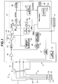
- FIGS. 1 to 10C A first embodiment of the present invention will be described with reference to FIGS. 1 to 10C.
- the electronic endoscope 2 has an elongated insert portion 6 to be inserted into a body cavity or the like, an operating portion 7 formed at the rear end (base end) of the insert portion 6, and a universal cable portion 8 extending from the operating portion 7.
- a connector 9 provided on the rear end of the universal cable portion 8 is detachably connected to the video processor 3.
- the CCD 15 in the system shown in FIG. 1 is a high-pixel CCD having a number of pixels about thrice the usual number of pixels. Accordingly, in this embodiment, the frequency of horizontal transfer pulses and reset pulses ⁇ R in this embodiment is set to a high frequency of about 30 MHz in contrast with that in the case of the usual number of pixels (about 10 MHz). While one electronic endoscope 2 is shown in FIG. 1, the signal processing system is formed by using a phase-locked loop (PLL) circuit 27 so that the video processor 3 shown in FIG. 1 is used in common with electronic endoscopes having different cable lengths including the length of the insert portion 6.
- PLL phase-locked loop
- reset pulses ⁇ R in the CCD drive signal for example are output in synchronization with a horizontal transfer signal or the like (not shown).
- a CCD output signal (image pickup signal) delayed, for example, by a time period Te from each reset pulse ⁇ R as shown in FIG. 2B is input to the FEA 18.
- a video signal period shown in an upper left section of FIG. 2A is a period during which the image pickup signal for a horizontal row of pixels in the CCD 15 is read out from the CCD 15.
- the waveform of the image pickup signal changes according to luminance information on the corresponding pixels.
- a phase adjustment period shown in an upper right section of FIG. 2A shows a non-signal period (empty signal period) after the completion of readout of the signal for the horizontal row of pixels in the CCD 15 (or before readout) during which no luminance information exists. Also during this period, reset pulses ⁇ R are applied to the CCD 15, as shown in FIG. 2A. As a result, the output signal from the CCD 15 is output as a reference clock for PLL circuit input, as shown in FIG. 2B.
- the duty ratio of reset pulses ⁇ R is changed in the phase adjustment period to facilitate separation from the video signal period.
- this is for facilitating separation between the two periods and is not indispensable for phase adjustment.
- the video signal period for read out of the signal for the next horizontal row of pixels follows the phase adjustment period shown in the right-hand section.
- the CCD 15 has predetermined numbers of pixels respectively arranged in horizontal and vertical directions.
- the video signal period is a period during which a horizontal row of pixels is read out by applying reset pulses ⁇ R or the like in the CCD drive signal in synchronization with a horizontal sync signal (abbreviated as HD in FIG. 3), and the phase adjustment period is an idle readout period immediately after the video signal period.
- the video signal period and the phase adjustment period thus recur.
- CCD output signals amplified by the FEA 18 are input to a correlative double sampling (CDS) and analog-to-digital (A/D) circuit 21.
- CDS correlative double sampling
- A/D analog-to-digital circuit 21.
- Signal portions in the image pickup signal are extracted and converted into a baseband signal by correlative double sampling in a CDS circuit portion.
- the baseband signal is converted into a digital signal in an A/D circuit portion.
- This digital signal is input to a post-video processing circuit 22.
- the post-video processing circuit 22 generates a video signal from this digital signal and outputs the video signal to the monitor 4.
- sampling pulses SP synchronized with a variable clock V-CLK output from the PLL circuit 27 described below are supplied from a sampling pulse generation circuit 23.
- the CDS circuit portion samples signal portions in image pickup signals.
- sampling pulses SP By using sampling pulses SP, a feed-through portion and luminance information portion in the image pickup signal shown in FIG. 2B are respectively sampled and a signal representing the difference therebetween is extracted, thereby forming the baseband signal.
- the CCD output signal amplified by the FEA 18 is passed through a band-pass filter (BPF) 24 band-restricted so as to extract reset pulses ⁇ R in the phase adjustment period (as a reference clock), and undergoes waveform shaping performed by a limiter amplifier 25.
- BPF band-pass filter
- the limiter amplifier 25 is constituted by, for example, an inverting amplifier A.
- a capacitor C for passage of an alternating current signal and a resistor R are connected between input and output terminals of the inverting amplifier A.
- the phase comparator 28 compares the phase of the reference clock R-CLK input thereto via the R-gate 26 and the variable clock V-CLK output from a voltage-controlled oscillator (abbreviated as VCXO) 30, and outputs a signal corresponding to the phase difference therebetween to a low-pass filter (LPF) 29.
- VCXO voltage-controlled oscillator
- the LPF 29 outputs to the VCXO 30 a signal formed of a low-frequency component of the output signal from the phase comparator 28. This signal is output as an output signal LPFout of the LPF 29.
- the VCXO 30 outputs the variable clock V-CLK whose oscillation frequency changes according to (for example, generally in proportion to) the voltage value of the output signal LPFout from the LPF 29 applied to its input end.
- the VCXO 30 outputs to the phase comparator 28 the variable clock V-CLK whose frequency or phase corresponds to the voltage value of the output signal LPFout from the LPF 29.
- the VCXO 30 also outputs the variable clock V-CLK to the sampling pulse generation circuit 23.
- the PLL circuit 27 is a circuit for generating sampling pulses SP according to suitable timing in an adjustment-free manner even in a case where the cable length is changed. Since the frequency of the reference clock R-CLK is substantially constant (determined by the number of pixels of the CCD 15), a crystal oscillating element having high frequency stability is used in the VCXO 30 to generate the variable clock V-CLK.
- the PLL circuit 27 is used for the purpose of phase-synchronizing the variable clock V-CLK with the phase of the reference clock R-CLK (the frequency of the reference clock R-CLK and the frequency of the variable clock V-CLK can therefore be considered to be substantially equal to each other even if the width of variation in which frequency of the variable clock V-CLK is changed is considered).
- the phase comparator 28 detects a timing discrepancy between the rising edges of the variable clock V-CLK and the rising edges of the reference clock R-CLK, i.e., the output timing phase difference between the two clocks.
- the phase comparator 28 outputs a signal corresponding to the phase difference to the LPF 29.
- the voltage value of the output signal LPFout from the LPF 29 decreases in correspondence with the phase difference and the oscillation frequency of the variable clock V-CLK is thereby reduced to delay the timing of the rising edges of the variable clock V-CLK (the phase of the variable clock V-CLK is delayed to reduce the phase difference).
- the oscillation frequency of the variable clock V-CLK of the VCXO 30 is increased (the phase of the variable clock V-CLK is advanced to reduce the phase difference).
- the frequency of the variable clock V-CLK is increased (that is, the phase is advanced).
- the R-gate 26 performs opening/closing control on the operation to input the reference clock R-CLK to the phase comparator 28 according to an R-gate opening/closing control signal Cgate from a field programmable gate array (FPGA) 31 constituting the reference signal generation circuit (SSG). That is, in this embodiment, selection between the state in which the reference clock R-CLK is input to the phase comparator 28 of the PLL circuit 27 and the state in which reference clock R-CLK is not input to the phase comparator 28 of the PLL circuit 27 is enabled to ensure that a frequency pull-in operation can be smoothly or rapidly performed by the PLL circuit 27.
- FPGA field programmable gate array
- This timing (also referred to as sync timing) is set so that the phase of the variable clock V-CLK (more specifically, the rising edge of the clock) is within a predetermined time period shorter than the cycle of the clock.
- frequency pull-in can be performed with stability when the frequency pull-in operation is first started, and that even in a case where the frequency pull-in ends in failure or pull-in is cancelled, the frequency pull-in operation by the PLL circuit 27 can be again performed in a suitable state by closing the R-gate 26 and by thereafter opening the R-gate 26.
- the R-gate opening/closing control signal Cgate is set to "opening" or “closing” (turned on/off), for example, in a period other than the phase adjustment period, as shown in FIG. 2C.
- the R-gate opening/closing control signal Cgate is set to "opening” (that is, the reference clock R-CLK to the phase comparator 28 is shut off) during some phase adjustment periods, as shown in FIG. 2C.
- the PLL circuit 27 is thereby set in such a state that the output signal LPFout from the LPF 29 sticks to the ground side.
- variable clock V-CLK is set (preset) in a most-delayed phase state corresponding to one end of a variable phase adjustment range (or a variable frequency range).
- the output signal LPFout from the LPF 29 is input to a sync detection circuit (or pull-in detection circuit) 32.
- the sync detection circuit 32 performs detection from the level of the output signal LPFout as to whether the PLL circuit 27 is in the phase-synchronized state, in the frequency pull-in state (locked) state or in the non-pull-in state ( unlock ), i.e., phase synchronization failure, and outputs the corresponding detection signal to the FPGA 31.
- the FPGA 31 inputs the detection signal from the sync detection circuit 32 to a counter circuit 31a which is, for example, provided in the FPGA 31, counts the number of clock pulses from the oscillator 35 by using the counter circuit 31a, and monitors the time period during which the phase synchronized state is maintained.
- the FPGA 31 performs the control operation including closing the R-gate 26 by setting the R-gate opening/closing control signal Cgate to "closing” (off), and thereafter opening the R-gate 26 by setting the R-gate opening/closing control signal Cgate to "opening" (on) to enable the reference clock R-CLK to be input to the phase comparator 28 of the PLL circuit 27.
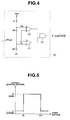
- FIG. 4 shows an example of a configuration of the sync detection circuit 32.
- the sync detection circuit 32 shown in FIG. 4 is constituted by a window comparator.
- a voltage VL obtained by dividing a power supply voltage Vdd between resistors R1 and R2 and a resistor R3 is applied.
- a voltage VH obtained by dividing the power supply voltage Vdd between the resistor R1 and the resistors R2 and R3 is applied.
- the window comparator When the level of the output signal LPFout from the LPF 29 is between the voltages VL and VH, the window comparator outputs the sync detection signal lock at "H".
- the sync detection circuit 32 outputs to the FPGA 31 the detection signal as to whether or not the PLL circuit 27 is in the pull-in state.
- the FPGA 31 monitors whether or not the PLL circuit 27 is in the synchronization state from the output signal from the sync detection circuit 32, and restarts the frequency pull-in operation again if the asynchronous state continues beyond the predetermined time period tc.
- the FPGA 31 outputs a control signal Cen to a latch circuit 33, whereby the intermittent operation control signal EN is applied to the phase comparator 28 as an operation control signal for starting the frequency pull-in operation by the PLL circuit 27.
- the control signal Cen is output so as to cover the intermittent phase adjustment period, as shown in FIG. 2D.
- the FPGA 31 and the latch circuit 33 form an operating control signal generation section for setting the PLL circuit 27 in the PLL operation state during the intermittent period.
- the control signal Cen becomes "H” and the intermittent operation control signal EN is applied from a Q output terminal of the latch circuit 33 to the phase comparator 28 by the timing with the delay time Ta of the delay circuit 34 from the timing of the rising edge of the variable clock V-CLK first output from the VCXO 30 after the timing by which the control signal Cen becomes "H".
- the phase comparator 28 then starts the phase comparison operation.
- the timing by which the intermittent operation control signal EN is applied to the phase comparator 28 is set by the delay circuit 34 and the latch circuit 33.
- the timing is set so that the intermittent operation control signal EN is synchronized with the timing of the rising edge of the variable clock V-CLK in the predetermined time period.
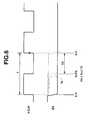
- This timing setting will be described with reference to FIG. 6.
- the input to the delay circuit 34 for setting the delay time X is the variable clock V-CLK in the case shown in FIG. 6.
- the reference clock R-CLK may be input in place of the variable clock V-CLK. (The value of the delay time X is changed in this case.)
- a low-band loop characteristic is set in order to stabilize the operation after frequency pull-in, i.e., to ensure a low-phase-noise characteristic.
- Ta is set to about T/4 ⁇ Ta ⁇ T/2 as shown in FIG. 6; a sync timing condition setting relaxed from the optimum condition is made.
- a sync timing setting is made such that the timing in the case of intermittently starting the frequency pull-in operation by the PLL circuit 27 (enabling the intermittent operation control signal EN ) and the variable clock V-CLK, i.e., a feedback signal to the phase comparator 28, are synchronized in a time period shorter than the cycle of the variable clock V-CLK.
- the constants of the LPF 29 are set so that the LPF 29 has a low-phase-noise low-band loop characteristic, thereby enabling a sync timing setting on a practical level to be made when frequency pull-in is performed and enabling frequency pull-in to be performed with stability by gate opening/closing by means of the gate section.
- the FPGA 31 generates the above-described control signal by using a reference clock generated by the oscillator 35 using a crystal oscillating element having high oscillation frequency stability, and supplies the CCD drive circuit 17 with a timing signal as a reference at the time of generation of the CCD drive signal.
- the power supply (not shown) for the video processor 3 is turned on.
- the FPGA 31 of the video processor 3 then becomes operable and sends to the CCD drive circuit 17 the timing signal synchronized with the horizontal sync signal.
- the CCD drive circuit 17 outputs to the CCD 15 the CCD drive signal including reset pulses ⁇ R during the video signal period, as shown in FIG. 2A.
- the FPGA 31 changes the R-gate opening/closing control signal Cgate from the off state to the on state by timing, for example, after the beginning of the first phase adjustment period, as shown in FIG. 2C, thereby establishing a state in which the reference clock R-CLK can be input to the phase comparator 28 via the R-gate 26.
- the intermittent operation control signal EN shown in FIG. 7D is applied from the latch circuit 33 to the phase comparator 28.
- the phase comparator 28 starts the phase comparison operation.
- the intermittent operation control signal shown in FIG. 7D also becomes “L” during each period Tcap corresponding generally to the phase adjustment period.
- the PLL circuit 27 performs the frequency pull-in operation during the time period Tcap continuing after beginning from the time at which the intermittent operation control signal EN first becomes “L” in each horizontal period as shown in FIG. 7D.
- FIG. 7E shows, by changing the time scale, the time periods during which the intermittent operation control signal EN intermittently (periodically) becomes “L” in every horizontal period (1H), and during which the frequency pull-in operation is performed.
- the R-gate opening/closing control signal Cgate changes from the off state to the on state, for example, after several or more recurrences of the intermittent operation control signal EN (the output signal LPFout from the LPF 29 sticking to the ground level in this state).
- the output signal LPFout from the LPF 29 is sticking to the ground side based on the reception of the result of phase detection by the phase comparator 28.
- the output signal LPFout from the LPF 29 rises toward the power supply voltage Vdd from the ground level, as shown in FIG. 8.
- a setting is made such that the fall timing of the intermittent operation control signal EN is synchronized with the variable clock V-CLK at about T/4 ⁇ Ta ⁇ T/2, as described above with reference to FIG. 6.
- the frequency of occurrence of input to the phase comparator 28 of one of the reference clock R-CLK and the variable clock V-CLK prior to the other in the asynchronous state will be considered. Since T/4 ⁇ Ta ⁇ T/2, the frequency of occurrence of input of the reference clock R-CLK prior to the variable clock V-CLK (in phase advance) is higher. Under this bias effect, the PLL loop operates to change the output signal LPFout toward the power supply voltage Vdd and to thereby advance the phase of the variable clock V-CLK.
- the output signal LPFout is changed by the bias effect based on Ta until a point in the vicinity of the frequency pull-in region is reached, and a transition to the PLL circuit capture process generally referred to is thereafter made to establish phase synchronization.
- Frequency pull-in is thus performed to hold the level of the output signal LPFout from the LPF 29 in the phase-synchronized state.
- the output signal LPFout from the LPF 29 is changed, for example, toward the power supply voltage level, as shown in FIG. 9A.
- the FPGA 31 changes the R-gate opening/closing control signal Cgate from the off state to the on state (see FIG. 9C).
- the output signal LPFout from the LPF 29 then rises from the ground level toward the power supply voltage Vdd, as described above with reference to FIG. 8. During this process, the frequency pull-in operation is smoothly performed.
- FIGS. 10A to 10C show an example of the operation in a case where frequency pull-in failure occurs when the operation shown in FIGS. 9A to 9C is performed.
- the FPGA 31 monitors the state of the output signal from the sync detection circuit 32, as described above. If, as shown in FIG. 10C, the out-of-synchronization state ( unlock state) continues, for example, for a predetermined time period td (e.g., about 200 mS) after the R-gate opening/closing control signal Cgate has been changed from the off state to the on state, the FPGA 31 returns the R-gate opening/ctosing control signal Cgate from the on state to the off state.
- td e.g., about 200 mS
- the FPGA 31 changes the R-gate opening/closing control signal Cgate from the off state to the on state after a lapse of time period toff to repeat frequency pull-in as described above with reference to FIGS. 9A to 9C.
- the sampling pulse generation circuit 23 supplied with the variable clock V-CLK phase-synchronized with the reference clock R-CLK outputs to the CDS and A/D circuit 21 sampling pulses SP for sampling the image pickup signal in the video signal period, thereby enabling the CDS and A/D circuit 21 to extract signal portions in the image pickup signal with stability by the signal portion extraction timing.
- Timing for extracting signal portions is thus performed with stability to obtain an endoscopic image of good image quality.
- frequency pull-in can be smoothly performed with a simple arrangement in a state where a low-band loop characteristic for a low phase noise characteristic is set.
- the low-band loop characteristic can be set substantially independently of the capture range. Therefore, the present invention is highly advantageous in a case where the phase comparison frequency is high and the iteration cycle of intermittent operation is long.
- the present invention can be implemented in a simple arrangement. Also, closed loop response can be set in a low-band loop characteristic for a low phase noise characteristic. Therefore, stable operation can be ensured after frequency pull-in and endoscopic images of good image quality can be successively obtained.
- the video processor 3C shown in FIG. 11 uses a PLL circuit 27C obtained by providing a frequency dividing circuit 53 in the PLL circuit 27 in the video processor 3 shown in FIG. 1.
- the frequency dividing ratio of the frequency dividing circuit 53 is variably set by the FPGA 31 according to the number of pixels in the ID information.
- the FPGA 31 also incorporates a frequency dividing circuit 54 which outputs to the CCD drive circuit 17 a timing signal frequency-divided by a frequency dividing ratio according to ID information including the number of pixels of the CCD 15 or 15B. That is, a common frequency dividing ratio is selected for the frequency dividing circuits 53 and 54 according to the number of pixels of the CCD actually driven.
- the FPGA 31 changes the delay time Ta of the delay circuit 34 when the reference clock R-CLK and the variable clock V-CLK are changed according to the number of pixels of the CCD. More specifically, for example, a delay time Ta inversely proportional to the frequency dividing ratio is selected and set. If the change in the number of pixels is not so large, the same delay time Ta may be used in common without being changed.
- the configuration is the same as that of the first embodiment.
- Components identical to those in the first embodiment are indicated by the same reference numerals, and the description for them will not be repeated.
- a CCD drive signal is generated which is frequency-divided by the frequency dividing circuit 54 to enable the CCD having the different number of pixels to be suitably driven, and the frequency dividing circuit 53 in the PLL circuit 27C on the signal processing side for processing on the image pickup signal correspondingly divides the variable clock V-CLK and to enable phase comparison in the phase comparator 28.
- the system in this embodiment can be suitably adapted to an electronic endoscope incorporating the CCD having a different number of pixels in an adjustment free manner, as is that in the first embodiment.
- This embodiment also ensures the same advantages as those in the first embodiment in other respects.
- a device for opening/closing the input path for reference clock R-CLK to (the phase comparator 28 in) the PLL circuit 27 or 27C is formed by using the R-gate 26 provided between the limiter amplifier 25 and the phase comparator 28.
- an arrangement such as that in an example of a modification shown in FIG. 12 may alternatively be adopted.
- FIG. 12 shows the configuration of an endoscope system 1B in an example of a modification of the first embodiment.
- the video processor 3B in the endoscope system 1B has a gate circuit corresponding to the R-gate 26. This gate circuit is disposed between the FPGA 31 and the CCD drive circuit 17 in the video processor 3 shown in FIG. 1.
- the R-gate opening/closing control signal Cgate and the intermittent operation control signal EN are input to an OR circuit 61, and an output signal from the OR circuit 61 is input to a NAND circuit 62.
- the timing signal for generating the CCD drive signal as in the case of the first embodiment is also input to the NAND circuit 62.
- An output from the NAND circuit 62 is input to the CCD drive circuit 17 via an inverter circuit 63.
- An AND circuit may be used in place of the NAND circuit 62 to remove the inverter circuit 63.
- the configuration is the same as that of the first embodiment.
- the gate formed by the NAND circuit 62 is open during a period when the intermittent operation control signal EN is "H", i.e., a video signal period defined by removing a time period in the vicinity of the phase adjustment period.
- the CCD 15 is driven in this video signal period in the same manner as in the first embodiment.
- the gate section performs an operation to open/close the input path for the reference clock R-CLK to the CCD drive circuit 17 in each phase adjustment period.
- the operation including frequency pull-in is substantially the same as that in the first embodiment. Also, substantially the same effects as those in the first embodiment are obtained.
- frequency pull-in can be performed with a simple arrangement in a state where a low-phase noise characteristic is set.
- the FPGA 31 closes the gate section and controls the phase state of the variable clock V-CLK so that the variable clock V-CLK is preset in the most delayed phase state in the phase adjustment range.
- the timing of enabling phase comparison of the intermittent operation control signal EN by the phase comparator 28 is set by being synchronized with T/2 or less (more preferably T/4 to T/2) of the cycle T of the clock rising edge of the variable clock V-CLK.
- This timing setting has the effect of changing the variable clock V-CLK in the direction of phase advance in terms of frequency.
- the timing of enabling phase comparison of the intermittent operation control signal EN by the phase comparator 28 is set by being synchronized with T/2 or more (more preferably T/2 to 3T/4) of the cycle T of the clock rising edge of the variable clock V-CLK.
- an offset voltage may be applied, for example, to the VCXO 30 according to the timing by which the gate section is closed. (Needless to say, the application of this offset voltage is stopped when the gate section is opened.)
Landscapes
- Health & Medical Sciences (AREA)
- Life Sciences & Earth Sciences (AREA)
- Surgery (AREA)
- Engineering & Computer Science (AREA)
- Biomedical Technology (AREA)
- Heart & Thoracic Surgery (AREA)
- Biophysics (AREA)
- Nuclear Medicine, Radiotherapy & Molecular Imaging (AREA)
- Optics & Photonics (AREA)
- Pathology (AREA)
- Radiology & Medical Imaging (AREA)
- Veterinary Medicine (AREA)
- Public Health (AREA)
- Physics & Mathematics (AREA)
- Medical Informatics (AREA)
- Molecular Biology (AREA)
- Animal Behavior & Ethology (AREA)
- General Health & Medical Sciences (AREA)
- Signal Processing (AREA)
- Multimedia (AREA)
- Endoscopes (AREA)
- Closed-Circuit Television Systems (AREA)
- Instruments For Viewing The Inside Of Hollow Bodies (AREA)
- Stabilization Of Oscillater, Synchronisation, Frequency Synthesizers (AREA)
Applications Claiming Priority (1)
| Application Number | Priority Date | Filing Date | Title |
|---|---|---|---|
| JP2005363695A JP4511454B2 (ja) | 2005-12-16 | 2005-12-16 | 内視鏡用信号処理装置 |
Publications (2)
| Publication Number | Publication Date |
|---|---|
| EP1798962A2 true EP1798962A2 (de) | 2007-06-20 |
| EP1798962A3 EP1798962A3 (de) | 2013-12-04 |
Family
ID=37806985
Family Applications (1)
| Application Number | Title | Priority Date | Filing Date |
|---|---|---|---|
| EP06025589.0A Withdrawn EP1798962A3 (de) | 2005-12-16 | 2006-12-11 | Endoskopsignalprozessor, Endoskopvorrichtung und Endoskopsignalverarbeitungsverfahren |
Country Status (3)
| Country | Link |
|---|---|
| US (1) | US8248464B2 (de) |
| EP (1) | EP1798962A3 (de) |
| JP (1) | JP4511454B2 (de) |
Cited By (3)
| Publication number | Priority date | Publication date | Assignee | Title |
|---|---|---|---|---|
| CN102781304A (zh) * | 2010-07-12 | 2012-11-14 | 奥林巴斯医疗株式会社 | 内窥镜图像处理装置和内窥镜系统 |
| US8934004B2 (en) | 2011-12-15 | 2015-01-13 | Olympus Medical Systems Corp. | Endoscope system |
| US9488910B2 (en) | 2009-12-14 | 2016-11-08 | Rohm And Haas Electronic Materials Llc | Sulfonyl photoacid generators and photoresists comprising same |
Families Citing this family (15)
| Publication number | Priority date | Publication date | Assignee | Title |
|---|---|---|---|---|
| JP5103913B2 (ja) * | 2007-01-30 | 2012-12-19 | ソニー株式会社 | 撮像装置及び映像信号発生装置 |
| JP2009201540A (ja) * | 2008-02-26 | 2009-09-10 | Fujinon Corp | 撮像システム及び内視鏡システム |
| JP5476876B2 (ja) * | 2009-09-11 | 2014-04-23 | 株式会社リコー | センサ駆動回路、ドライバ装置、画像読取装置、及び画像形成装置 |
| JP5767036B2 (ja) | 2011-06-20 | 2015-08-19 | オリンパス株式会社 | 電子内視鏡装置 |
| JP5784382B2 (ja) * | 2011-06-20 | 2015-09-24 | オリンパス株式会社 | 電子内視鏡装置 |
| JP5745961B2 (ja) * | 2011-07-15 | 2015-07-08 | オリンパス株式会社 | 電子内視鏡装置 |
| US9332193B2 (en) * | 2011-11-14 | 2016-05-03 | Omnivision Technologies, Inc. | Synchronization of image acquisition in multiple image sensors with a synchronization clock signal |
| JP2014124493A (ja) * | 2012-12-27 | 2014-07-07 | Olympus Medical Systems Corp | 内視鏡システム |
| JP6173766B2 (ja) * | 2013-05-10 | 2017-08-02 | Hoya株式会社 | 電子内視鏡用プロセッサ、電子内視鏡システムおよび画像処理装置 |
| US9525852B2 (en) | 2013-08-02 | 2016-12-20 | General Electric Company | Systems and methods for embedded imaging clocking |
| JP6747871B2 (ja) * | 2016-05-23 | 2020-08-26 | オリンパス株式会社 | 撮像装置 |
| KR102500291B1 (ko) * | 2016-09-05 | 2023-02-16 | 삼성전자주식회사 | 통신 인터페이스 장치 및 디스플레이 장치 |
| WO2020144777A1 (ja) * | 2019-01-09 | 2020-07-16 | オリンパス株式会社 | 撮像素子、内視鏡および制御装置 |
| DE102021116905A1 (de) | 2021-06-30 | 2023-01-05 | Ambu A/S | Rauschenerkennungsschaltung |
| WO2023275177A1 (en) * | 2021-06-30 | 2023-01-05 | Ambu A/S | Video processing apparatus with noise effect mitigation |
Citations (4)
| Publication number | Priority date | Publication date | Assignee | Title |
|---|---|---|---|---|
| US4860095A (en) | 1987-04-21 | 1989-08-22 | Olympus Optical Co., Ltd. | Video camera apparatus and video endoscope apparatus with means for compensating image errors caused by differing cable lengths |
| US5285483A (en) | 1992-04-07 | 1994-02-08 | Seiko Epson Corporation | Phase synchronization circuit |
| JPH0686138A (ja) | 1992-06-11 | 1994-03-25 | Olympus Optical Co Ltd | 画像撮像装置 |
| US5585840A (en) | 1992-06-11 | 1996-12-17 | Olympus Optical Co., Ltd. | Endoscope apparatus in which image pickup means and signal control means are connected to each other by signal transmitting means |
Family Cites Families (11)
| Publication number | Priority date | Publication date | Assignee | Title |
|---|---|---|---|---|
| US4262258A (en) * | 1979-02-06 | 1981-04-14 | Nasa | CCD Correlated quadruple sampling processor |
| JPH04370581A (ja) * | 1991-06-18 | 1992-12-22 | Ricoh Co Ltd | Pll回路 |
| JPH05122058A (ja) | 1991-10-24 | 1993-05-18 | Kokusai Electric Co Ltd | デイジタル位相同期回路 |
| JPH08265150A (ja) * | 1995-03-22 | 1996-10-11 | Asahi Kasei Micro Syst Kk | 位相同期発振回路 |
| JPH0962222A (ja) | 1995-08-23 | 1997-03-07 | Seiko Epson Corp | ドットクロック再生回路 |
| US6466256B1 (en) * | 1996-04-05 | 2002-10-15 | Asahi Kogaku Kogyo Kabushiki Kaisha | Video-signal processing device connectable to an electronic endoscope |
| JP3263621B2 (ja) * | 1997-01-23 | 2002-03-04 | 三洋電機株式会社 | Pll回路 |
| JP3810185B2 (ja) * | 1997-08-06 | 2006-08-16 | 大井電気株式会社 | 同期発振回路 |
| JP2000165759A (ja) | 1998-11-24 | 2000-06-16 | Olympus Optical Co Ltd | 内視鏡撮像装置 |
| JP4079733B2 (ja) * | 2002-09-26 | 2008-04-23 | Necエレクトロニクス株式会社 | 位相同期ループ回路 |
| KR100532498B1 (ko) * | 2004-01-28 | 2005-11-30 | 삼성전자주식회사 | 오실레이터와 카운터를 이용하는 지연 동기 회로 및 클럭동기 방법 |
-
2005
- 2005-12-16 JP JP2005363695A patent/JP4511454B2/ja not_active Expired - Fee Related
-
2006
- 2006-12-11 EP EP06025589.0A patent/EP1798962A3/de not_active Withdrawn
- 2006-12-14 US US11/638,755 patent/US8248464B2/en active Active
Patent Citations (4)
| Publication number | Priority date | Publication date | Assignee | Title |
|---|---|---|---|---|
| US4860095A (en) | 1987-04-21 | 1989-08-22 | Olympus Optical Co., Ltd. | Video camera apparatus and video endoscope apparatus with means for compensating image errors caused by differing cable lengths |
| US5285483A (en) | 1992-04-07 | 1994-02-08 | Seiko Epson Corporation | Phase synchronization circuit |
| JPH0686138A (ja) | 1992-06-11 | 1994-03-25 | Olympus Optical Co Ltd | 画像撮像装置 |
| US5585840A (en) | 1992-06-11 | 1996-12-17 | Olympus Optical Co., Ltd. | Endoscope apparatus in which image pickup means and signal control means are connected to each other by signal transmitting means |
Cited By (6)
| Publication number | Priority date | Publication date | Assignee | Title |
|---|---|---|---|---|
| US9488910B2 (en) | 2009-12-14 | 2016-11-08 | Rohm And Haas Electronic Materials Llc | Sulfonyl photoacid generators and photoresists comprising same |
| US10466588B2 (en) | 2009-12-14 | 2019-11-05 | Rohm And Haas Electronic Materials Llc | Sulfonyl photoacid generators and photoresists comprising same |
| CN102781304A (zh) * | 2010-07-12 | 2012-11-14 | 奥林巴斯医疗株式会社 | 内窥镜图像处理装置和内窥镜系统 |
| EP2520215A4 (de) * | 2010-07-12 | 2013-05-22 | Olympus Medical Systems Corp | Vorrichtung zur verarbeitung von endoskopbildern und endoskopsystem |
| CN102781304B (zh) * | 2010-07-12 | 2015-01-21 | 奥林巴斯医疗株式会社 | 内窥镜图像处理装置和内窥镜系统 |
| US8934004B2 (en) | 2011-12-15 | 2015-01-13 | Olympus Medical Systems Corp. | Endoscope system |
Also Published As
| Publication number | Publication date |
|---|---|
| EP1798962A3 (de) | 2013-12-04 |
| US20070139521A1 (en) | 2007-06-21 |
| JP4511454B2 (ja) | 2010-07-28 |
| US8248464B2 (en) | 2012-08-21 |
| JP2007159991A (ja) | 2007-06-28 |
Similar Documents
| Publication | Publication Date | Title |
|---|---|---|
| US8248464B2 (en) | Endoscope signal processor, endoscope apparatus and endoscope signal processing method | |
| US8035684B2 (en) | Image-signal generating apparatus | |
| US7248281B2 (en) | Electronic endoscope apparatus which superimposes signals on power supply | |
| US5585840A (en) | Endoscope apparatus in which image pickup means and signal control means are connected to each other by signal transmitting means | |
| JP5331947B1 (ja) | 内視鏡システム | |
| US7355625B1 (en) | Endoscopic imaging system and endoscope system | |
| US5434615A (en) | Signal processing circuit adaptable to electronic endoscopes having different lengths | |
| EP2094002A2 (de) | Elektronisches Kommunikationssystem und Endoskopsystem | |
| EP2537454A2 (de) | Elektronisches Endoskopgerät | |
| US5226063A (en) | Counter for an image pickup system | |
| JP7039733B2 (ja) | 撮像システム | |
| JP4141757B2 (ja) | 電子内視鏡装置 | |
| US4737848A (en) | Driving apparatus for charge-coupled image sensor producing controlled transfer pulses | |
| EP0454153B1 (de) | Synchronisierschaltung | |
| JP4315538B2 (ja) | 内視鏡システム | |
| JPH08280611A (ja) | 電子内視鏡装置 | |
| JP4187486B2 (ja) | 電子内視鏡装置 | |
| JP2014124493A (ja) | 内視鏡システム | |
| JP2001275954A (ja) | 電子内視鏡装置 | |
| JPH09154068A (ja) | 固体撮像装置 | |
| JP3642953B2 (ja) | ヘッド分離型ccdカメラの同期調整方法 | |
| JPH10322604A (ja) | 固体撮像装置 | |
| JP4233551B2 (ja) | タイミング制御装置およびタイミング制御方法 | |
| KR20000051872A (ko) | 감시시스템의 동기화 장치 | |
| JP2517441B2 (ja) | テレビカメラの同期回路 |
Legal Events
| Date | Code | Title | Description |
|---|---|---|---|
| PUAI | Public reference made under article 153(3) epc to a published international application that has entered the european phase |
Free format text: ORIGINAL CODE: 0009012 |
|
| 17P | Request for examination filed |
Effective date: 20061211 |
|
| AK | Designated contracting states |
Kind code of ref document: A2 Designated state(s): AT BE BG CH CY CZ DE DK EE ES FI FR GB GR HU IE IS IT LI LT LU LV MC NL PL PT RO SE SI SK TR |
|
| AX | Request for extension of the european patent |
Extension state: AL BA HR MK YU |
|
| PUAL | Search report despatched |
Free format text: ORIGINAL CODE: 0009013 |
|
| AK | Designated contracting states |
Kind code of ref document: A3 Designated state(s): AT BE BG CH CY CZ DE DK EE ES FI FR GB GR HU IE IS IT LI LT LU LV MC NL PL PT RO SE SI SK TR |
|
| AX | Request for extension of the european patent |
Extension state: AL BA HR MK RS |
|
| RIC1 | Information provided on ipc code assigned before grant |
Ipc: A61B 1/045 20060101ALN20131031BHEP Ipc: H04N 5/225 20060101ALI20131031BHEP Ipc: H04N 5/232 20060101AFI20131031BHEP |
|
| AKX | Designation fees paid |
Designated state(s): DE FR GB |
|
| 17Q | First examination report despatched |
Effective date: 20140917 |
|
| RAP1 | Party data changed (applicant data changed or rights of an application transferred) |
Owner name: OLYMPUS CORPORATION |
|
| RAP1 | Party data changed (applicant data changed or rights of an application transferred) |
Owner name: OLYMPUS CORPORATION |
|
| RAP1 | Party data changed (applicant data changed or rights of an application transferred) |
Owner name: OLYMPUS CORPORATION |
|
| STAA | Information on the status of an ep patent application or granted ep patent |
Free format text: STATUS: EXAMINATION IS IN PROGRESS |
|
| STAA | Information on the status of an ep patent application or granted ep patent |
Free format text: STATUS: THE APPLICATION IS DEEMED TO BE WITHDRAWN |
|
| 18D | Application deemed to be withdrawn |
Effective date: 20170103 |