EP1801880A2 - Organische elektrolumineszente Vorrichtung mit Scanlinien identischen Widerstandes - Google Patents
Organische elektrolumineszente Vorrichtung mit Scanlinien identischen Widerstandes Download PDFInfo
- Publication number
- EP1801880A2 EP1801880A2 EP06018860A EP06018860A EP1801880A2 EP 1801880 A2 EP1801880 A2 EP 1801880A2 EP 06018860 A EP06018860 A EP 06018860A EP 06018860 A EP06018860 A EP 06018860A EP 1801880 A2 EP1801880 A2 EP 1801880A2
- Authority
- EP
- European Patent Office
- Prior art keywords
- scan line
- electroluminescent device
- organic electroluminescent
- scan
- scan lines
- Prior art date
- Legal status (The legal status is an assumption and is not a legal conclusion. Google has not performed a legal analysis and makes no representation as to the accuracy of the status listed.)
- Ceased
Links
Images



Classifications
-
- H—ELECTRICITY
- H10—SEMICONDUCTOR DEVICES; ELECTRIC SOLID-STATE DEVICES NOT OTHERWISE PROVIDED FOR
- H10K—ORGANIC ELECTRIC SOLID-STATE DEVICES
- H10K59/00—Integrated devices, or assemblies of multiple devices, comprising at least one organic light-emitting element covered by group H10K50/00
- H10K59/10—OLED displays
- H10K59/17—Passive-matrix OLED displays
- H10K59/179—Interconnections, e.g. wiring lines or terminals
-
- H—ELECTRICITY
- H05—ELECTRIC TECHNIQUES NOT OTHERWISE PROVIDED FOR
- H05B—ELECTRIC HEATING; ELECTRIC LIGHT SOURCES NOT OTHERWISE PROVIDED FOR; CIRCUIT ARRANGEMENTS FOR ELECTRIC LIGHT SOURCES, IN GENERAL
- H05B33/00—Electroluminescent light sources
- H05B33/12—Light sources with substantially two-dimensional [2D] radiating surfaces
- H05B33/26—Light sources with substantially two-dimensional [2D] radiating surfaces characterised by the composition or arrangement of the conductive material used as an electrode
Definitions
- the present invention relates to an organic electroluminescent device, particularly relates to an organic electroluminescent device which can be driven stably by scan lines having the same resistance values.
- Organic electroluminescence is the phenomenon which excitons are formed in an (low molecular or high molecular) organic material thin film by re-combining holes injected through an anode with electrons injected through a cathode, and light with specific wavelength is generated.
- the organic electroluminescent device using the above phenomenon has a basic structure as illustrated in Fig. 1.
- the basic structure of the organic electroluminescent device includes a glass substrate 200, an indium-tin-oxide layer 102 (hereinafter, referred as "ITO layer") formed on the upper side of the glass substrate 200 and acting as anode electrode, an insulating layer, an organic material layer, and a metal layer 104 acting as cathode electrode in the order. Walls (not shown) are formed to deposit the metal layers 104 separately on the ITO layer 102.
- ITO layer indium-tin-oxide layer
- Fig. 2 is a sectional view of the organic electroluminescent device shown in Fig. 1 and shows that a cap 106 is bonded to the substrate 200 as shown in Fig. 1.
- a plurality of data lines 111 and scan lines 110a and 110b are formed on an outer portion of an active area 100 including a plurality of ITO layers 102 (anode electrodes) and a plurality of metal layers 104 (cathode electrodes).
- the data lines 111 and the scan lines 110a and 110b are connected electrically to the anode electrodes 102 and the cathode electrodes 104.
- reference numeral "108" which is not described indicates a moisture absorbent sheet (so called as "getter”) attached to an inner surface of the cap 106 through an adhesive 107.
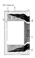
- Fig. 3 is a plane view of an entire organic electroluminescent device shown in Fig. 1 except the cap 106 and shows a configuration of the actual organic electroluminescent device.
- a plurality of data lines 111 connected to the anode electrodes 102 in the active area 100, respectively, have the same length practically and end portions thereof are arranged on a connecting section P.
- a plurality of scan lines 110a and 110b connected to ends of the cathode electrodes 104 are extended outsides of the active area 100 and then disposed on the connecting section P formed at a location adjacent to the active area 100 through an end portion thereof.
- the lengths of the scan lines 110a and 110b differ from each other according to the locations thereof, consequently, resistances of the scan lines are different from each other.
- the data current is flow to a ground through the data line, the pixel and the scan lines, and so the resistance of scan line has influence on the cathode voltage of the corresponding pixel (that is, a brightness of the pixel).
- the pixels emit the lights with the brightness which differ from each other. Consequently, different resistances of the scan lines cause a brightness difference among the pixels when the display device is operated, and due to the above phenomenon, the display failure is generated.
- the present invention is conceived to solve the above problem caused by a resistance difference among the scan lines constituting the organic electroluminescent device, an object of the present invention is to provide the organic electroluminescent device in which a plurality of scan lines are arranged to maintain identically resistances of the scan lines.
- the organic electroluminescent device comprises an active area consisting of anode electrodes, organic material layer and cathode electrodes; data lines connected to the anode electrodes for transmitting electrical signal to the anode electrodes; and scan lines connected to the cathode electrodes for transmitting electrical signal to the cathodes, wherein each scan line has a length which is the same as that (those) of neighboring scan line(s).
- the scan line has at least one portion which is bent with a certain angle, and the bending frequency of one scan line is more than that of the scan line formed at an outer side thereof. Also, the bending angle of the bent portion of one scan line is smaller than that of the scan line formed at an outer side thereof.
- each of the scan lines can have at least one curved portion.
- the curved portion of one scan line is smaller than that of the curved portion of the scan line formed at an outer side thereof.
- Fig. 1 is a plane view illustrating schematically a basic structure of organic electroluminescent device
- Fig. 2 is a sectional view of an organic electroluminescent device, shown in Fig. 1, on which a cap is bonded;
- Fig. 3 is a plane view of an entire organic electroluminescent device shown in Fig. 1;
- Fig. 4 is a plane view illustrating schematically a basic structure of the organic electroluminescent device according to the present invention.
- Fig. 5 is a detail view corresponding to "A" section of Fig. 3 and shows only some of scan lines constituting the organic electroluminescent device shown in FIG. 4;
- Fig. 6 is a view corresponding to Fig. 5 and shows another configuration of the scan lines constituting the organic electroluminescent device according to the present invention.
- the organic electroluminescent device is provided as an example of the light emitting device. It is, however, obvious that the teaching of the present invention is not limited to the organic electroluminescent device.
- a plurality of data lines 311 and scan lines 310a and 310b are formed on an outside of an active area 300 on which anode electrodes 302 and cathode electrodes 304 are formed.
- the data lines 311 and the scan lines 310a and 310b are connected electrically to the anode electrodes 302 and the cathode electrodes 304.
- a plurality of data lines 311 connected to the anode electrodes 302 in the active area 300, respectively, have the same length practically and end portions thereof are arranged on a connecting section P.
- the most import feature of the present invention is that the scan lines 310a and 310b have non-linear sections such that the lengths of the scan lines are the same, and so all the scan lines have the same resistance.
- Fig. 5 is a detail view corresponding to "A" section of Fig. 3 and shows only some of the scan lines constituting the organic electroluminescent device according to the present invention.
- reference numerals 310a-1, 310a-2 ... 310a-n indicate the scan lines.
- the innermost scan line 310a-1 (hereinafter, referred to as "first scan line") formed on an area which is most adjacent to the active area ( 300 in Fig. 4) is bent several times, and the scan line 310a-2 (second scan line) formed on an outside of the first scan line 310a-1 is also bent several time.
- a bending angle of each bent portion of the second scan line 310a-2 is larger than that of the first scan line 310a-1, and the bending frequency of the second scan line 310a-2 can be less than that of the first scan line 310a-1. Accordingly, the entire length of the second scan line 310a-2 is the same as that of the first scan line 310a-1 .
- a length of any one scan line becomes identical to that (those) of the neighboring scan line(s), and so all the scan lines 310a-1, 310a-2 ... 310a-n have the same length and the same resistance.
- end portions of the scan lines 310a-1, 310a-2 ... 310a-n should be disposed on the connecting section ( P in Fig. 4).
- Fig. 5 shows that all the scan lines 310a-1, 310a-2 ... 110a-n have the same length by bending the scan lines at a certain angle
- the configuration of the scan lines is not limited to that shown in Fig. 5.
- Fig. 6 is a view corresponding to Fig. 5 and shows another configuration of the scan lines constituting the organic electroluminescent device according to the present invention.
- each of the scan lines 320a-1, 320a-2 ... 320a-n can have at least one curved shaped portion.
- the radius of curvatures of curved portions of the scan lines 320a-1, 320a-2 ... 320a-n differ from each other.
- a radius of curvature of a curved portion of any one scan line is less than that of the second scan line 320a-2 formed at an outer side of the first scan line 320a-1.
- a length of any one scan line becomes identical to that (those) of the neighboring scan line(s), and so all the scan lines 320a-1, 320a-2 ... 320a-n have the same length and the same resistance.
- end portions of the scan lines 320a-1, 320a-2 ... 320a-n should be disposed on the connecting section ( P in Fig. 4).
- Fig. 4 shows the configuration of the organic electroluminescent device in which the scan lines 310a, 310b connected to the cathode electrodes 304 are extended alternatively from both sides of the active area 300
- the present is applicable to the organic electroluminescent device having the configuration in which all the scan lines are extended from only one side of the active area.
- the present is applicable to the organic electroluminescent device in which some scan lines connected to the cathode electrodes disposed on a first region of the active area are extended from one side of the active area and remainder of the scan lines connected to the cathode electrodes formed on a second region of the active area are extended from the other side of the active area.
- all the metal lines have the same length and the same resistance.
- a cathode voltage of the first pixel associated with the first scan line is substantially identical with a cathode voltage of the second pixel associated with the second scan line and corresponding to the second pixel in a magnitude. Consequently, if the data current with the same magnitude are applied to the first and second pixels, the first and second pixels emit the light with the same brightness when the display device is operated.
Landscapes
- Electroluminescent Light Sources (AREA)
- Devices For Indicating Variable Information By Combining Individual Elements (AREA)
Applications Claiming Priority (1)
| Application Number | Priority Date | Filing Date | Title |
|---|---|---|---|
| KR1020050127955A KR100775827B1 (ko) | 2005-12-22 | 2005-12-22 | 균일한 저항값을 갖는 스캔 라인을 포함한 유기 전계 발광소자 |
Publications (2)
| Publication Number | Publication Date |
|---|---|
| EP1801880A2 true EP1801880A2 (de) | 2007-06-27 |
| EP1801880A3 EP1801880A3 (de) | 2011-03-09 |
Family
ID=37907470
Family Applications (1)
| Application Number | Title | Priority Date | Filing Date |
|---|---|---|---|
| EP06018860A Ceased EP1801880A3 (de) | 2005-12-22 | 2006-09-08 | Organische elektrolumineszente Vorrichtung mit Scanlinien identischen Widerstandes |
Country Status (5)
| Country | Link |
|---|---|
| US (1) | US20070159081A1 (de) |
| EP (1) | EP1801880A3 (de) |
| JP (1) | JP2007173213A (de) |
| KR (1) | KR100775827B1 (de) |
| CN (1) | CN100477870C (de) |
Families Citing this family (10)
| Publication number | Priority date | Publication date | Assignee | Title |
|---|---|---|---|---|
| KR101249246B1 (ko) * | 2006-06-27 | 2013-04-01 | 삼성디스플레이 주식회사 | 표시 기판 및 이를 구비한 표시 장치 |
| JP4533963B2 (ja) * | 2008-05-01 | 2010-09-01 | フジテック・インターナショナル株式会社 | 有機el発光装置 |
| KR101750022B1 (ko) * | 2013-08-21 | 2017-06-22 | 엘지디스플레이 주식회사 | 유기전계발광표시장치 |
| US9356087B1 (en) | 2014-12-10 | 2016-05-31 | Lg Display Co., Ltd. | Flexible display device with bridged wire traces |
| KR102262667B1 (ko) * | 2015-01-22 | 2021-06-08 | 엘지디스플레이 주식회사 | Led 어레이 및 이를 포함하는 액정표시장치 |
| CN104637834B (zh) * | 2015-03-03 | 2017-04-19 | 京东方科技集团股份有限公司 | 数据线合格性测试方法和装置、阵列基板及其制作方法 |
| US20200103991A1 (en) * | 2018-09-29 | 2020-04-02 | Wuhan China Star Optoelectronics Technology Co., Ltd. | Display panel, display module and electronic device |
| WO2020227861A1 (zh) * | 2019-05-10 | 2020-11-19 | 京东方科技集团股份有限公司 | 发光驱动基板及其制作方法、发光基板和显示装置 |
| CN110068972A (zh) * | 2019-05-30 | 2019-07-30 | 深圳晶华显示器材有限公司 | 一种液晶显示屏及其驱动方法 |
| CN114975517A (zh) * | 2021-02-22 | 2022-08-30 | 京东方科技集团股份有限公司 | 显示基板、显示装置和布线方法 |
Family Cites Families (14)
| Publication number | Priority date | Publication date | Assignee | Title |
|---|---|---|---|---|
| JPH0198846A (ja) * | 1987-10-09 | 1989-04-17 | Sharp Corp | 蓄熱装置 |
| KR100237679B1 (ko) * | 1995-12-30 | 2000-01-15 | 윤종용 | 저항 차를 줄이는 팬 아웃부를 가지는 액정 표시 패널 |
| JPH1063198A (ja) * | 1996-08-19 | 1998-03-06 | Denso Corp | マトリクス型el表示装置 |
| US6111357A (en) * | 1998-07-09 | 2000-08-29 | Eastman Kodak Company | Organic electroluminescent display panel having a cover with radiation-cured perimeter seal |
| US6228228B1 (en) * | 1999-02-23 | 2001-05-08 | Sarnoff Corporation | Method of making a light-emitting fiber |
| KR20020027958A (ko) * | 2000-10-06 | 2002-04-15 | 구자홍 | 표시소자의 cof 구조 |
| JP2003005670A (ja) * | 2001-06-20 | 2003-01-08 | Toshiba Corp | 平面表示装置 |
| KR100434276B1 (ko) * | 2001-08-21 | 2004-06-05 | 엘지전자 주식회사 | 유기 el 소자 |
| JP2003140181A (ja) * | 2001-11-02 | 2003-05-14 | Nec Corp | 液晶表示装置 |
| TW510061B (en) * | 2001-12-31 | 2002-11-11 | Windell Corp | Layout structure of the electrode pin of organic light emitting diode |
| JP3925486B2 (ja) * | 2003-01-23 | 2007-06-06 | セイコーエプソン株式会社 | 電気光学装置用基板、電気光学装置及び電子機器 |
| TW583446B (en) * | 2003-05-28 | 2004-04-11 | Chunghwa Picture Tubes Ltd | Conducting line structure of a liquid crystal display |
| JP4439988B2 (ja) * | 2004-04-23 | 2010-03-24 | シャープ株式会社 | 表示装置 |
| KR100649171B1 (ko) * | 2005-10-18 | 2006-11-27 | 주식회사 대우일렉트로닉스 | 유기 el 디스플레이 장치 |
-
2005
- 2005-12-22 KR KR1020050127955A patent/KR100775827B1/ko not_active Expired - Lifetime
-
2006
- 2006-09-06 US US11/515,793 patent/US20070159081A1/en not_active Abandoned
- 2006-09-08 EP EP06018860A patent/EP1801880A3/de not_active Ceased
- 2006-09-19 CN CNB2006101539880A patent/CN100477870C/zh active Active
- 2006-10-10 JP JP2006276471A patent/JP2007173213A/ja active Pending
Also Published As
| Publication number | Publication date |
|---|---|
| KR100775827B1 (ko) | 2007-11-13 |
| EP1801880A3 (de) | 2011-03-09 |
| KR20070066580A (ko) | 2007-06-27 |
| JP2007173213A (ja) | 2007-07-05 |
| US20070159081A1 (en) | 2007-07-12 |
| CN100477870C (zh) | 2009-04-08 |
| CN1988744A (zh) | 2007-06-27 |
Similar Documents
| Publication | Publication Date | Title |
|---|---|---|
| JP7522155B2 (ja) | 発光装置、及びこれを備えた表示装置 | |
| KR102516131B1 (ko) | 표시 장치 및 그의 제조 방법 | |
| KR102705346B1 (ko) | 발광 장치, 그의 제조 방법, 및 이를 구비한 표시 장치 | |
| US12334478B2 (en) | Light emitting device and display device having same | |
| US9351349B2 (en) | Organic EL device having improved sealing property | |
| JP4931783B2 (ja) | 有機el表示パネル | |
| JP4968967B2 (ja) | 発光装置 | |
| JP6640599B2 (ja) | 表示装置 | |
| US10754181B2 (en) | Flexible display panel and manufacturing method thereof, and display device | |
| EP1801880A2 (de) | Organische elektrolumineszente Vorrichtung mit Scanlinien identischen Widerstandes | |
| CN211654825U (zh) | 阵列基板、显示面板及其走线结构 | |
| CN109671751B (zh) | 显示装置、显示面板及其制造方法 | |
| US7205572B2 (en) | Organic electroluminescent display device | |
| KR100611162B1 (ko) | 유기전계발광 표시장치 | |
| JP2004200041A (ja) | 有機el表示装置 | |
| JP5471317B2 (ja) | 有機elパネル | |
| JP4439988B2 (ja) | 表示装置 | |
| KR20060064685A (ko) | 유기 일렉트로루미네슨스 표시 패널 | |
| JP5477626B2 (ja) | 有機elモジュール | |
| JP2009076341A (ja) | 有機elディスプレイ | |
| JP2003092190A (ja) | 有機エレクトロルミネセンス素子及びその製造方法 | |
| JP2003142258A (ja) | 有機elパネル | |
| KR100708687B1 (ko) | 유기전계 발광소자 및 그의 제조방법 | |
| JP4395996B2 (ja) | 表示パネル | |
| CN102623645A (zh) | 有机电致发光元件 |
Legal Events
| Date | Code | Title | Description |
|---|---|---|---|
| PUAI | Public reference made under article 153(3) epc to a published international application that has entered the european phase |
Free format text: ORIGINAL CODE: 0009012 |
|
| 17P | Request for examination filed |
Effective date: 20060908 |
|
| AK | Designated contracting states |
Kind code of ref document: A2 Designated state(s): AT BE BG CH CY CZ DE DK EE ES FI FR GB GR HU IE IS IT LI LT LU LV MC NL PL PT RO SE SI SK TR |
|
| AX | Request for extension of the european patent |
Extension state: AL BA HR MK YU |
|
| RAP1 | Party data changed (applicant data changed or rights of an application transferred) |
Owner name: LG DISPLAY CO., LTD. |
|
| RAP1 | Party data changed (applicant data changed or rights of an application transferred) |
Owner name: LG DISPLAY CO., LTD. |
|
| PUAL | Search report despatched |
Free format text: ORIGINAL CODE: 0009013 |
|
| AK | Designated contracting states |
Kind code of ref document: A3 Designated state(s): AT BE BG CH CY CZ DE DK EE ES FI FR GB GR HU IE IS IT LI LT LU LV MC NL PL PT RO SE SI SK TR |
|
| AX | Request for extension of the european patent |
Extension state: AL BA HR MK RS |
|
| AKX | Designation fees paid |
Designated state(s): AT BE BG CH CY CZ DE DK EE ES FI FR GB GR HU IE IS IT LI LT LU LV MC NL PL PT RO SE SI SK TR |
|
| 17Q | First examination report despatched |
Effective date: 20120917 |
|
| STAA | Information on the status of an ep patent application or granted ep patent |
Free format text: STATUS: THE APPLICATION HAS BEEN REFUSED |
|
| 18R | Application refused |
Effective date: 20150704 |