EP1801895B1 - MTJ MgO/NiFe pour application MRAM haute performance - Google Patents
MTJ MgO/NiFe pour application MRAM haute performance Download PDFInfo
- Publication number
- EP1801895B1 EP1801895B1 EP06392019.3A EP06392019A EP1801895B1 EP 1801895 B1 EP1801895 B1 EP 1801895B1 EP 06392019 A EP06392019 A EP 06392019A EP 1801895 B1 EP1801895 B1 EP 1801895B1
- Authority
- EP
- European Patent Office
- Prior art keywords
- layer
- mgo
- mtj
- magnesium
- thickness
- Prior art date
- Legal status (The legal status is an assumption and is not a legal conclusion. Google has not performed a legal analysis and makes no representation as to the accuracy of the status listed.)
- Active
Links
Images

Classifications
-
- H—ELECTRICITY
- H10—SEMICONDUCTOR DEVICES; ELECTRIC SOLID-STATE DEVICES NOT OTHERWISE PROVIDED FOR
- H10N—ELECTRIC SOLID-STATE DEVICES NOT OTHERWISE PROVIDED FOR
- H10N50/00—Galvanomagnetic devices
- H10N50/01—Manufacture or treatment
-
- B—PERFORMING OPERATIONS; TRANSPORTING
- B82—NANOTECHNOLOGY
- B82Y—SPECIFIC USES OR APPLICATIONS OF NANOSTRUCTURES; MEASUREMENT OR ANALYSIS OF NANOSTRUCTURES; MANUFACTURE OR TREATMENT OF NANOSTRUCTURES
- B82Y25/00—Nanomagnetism, e.g. magnetoimpedance, anisotropic magnetoresistance, giant magnetoresistance or tunneling magnetoresistance
-
- B—PERFORMING OPERATIONS; TRANSPORTING
- B82—NANOTECHNOLOGY
- B82Y—SPECIFIC USES OR APPLICATIONS OF NANOSTRUCTURES; MEASUREMENT OR ANALYSIS OF NANOSTRUCTURES; MANUFACTURE OR TREATMENT OF NANOSTRUCTURES
- B82Y40/00—Manufacture or treatment of nanostructures
-
- C—CHEMISTRY; METALLURGY
- C23—COATING METALLIC MATERIAL; COATING MATERIAL WITH METALLIC MATERIAL; CHEMICAL SURFACE TREATMENT; DIFFUSION TREATMENT OF METALLIC MATERIAL; COATING BY VACUUM EVAPORATION, BY SPUTTERING, BY ION IMPLANTATION OR BY CHEMICAL VAPOUR DEPOSITION, IN GENERAL; INHIBITING CORROSION OF METALLIC MATERIAL OR INCRUSTATION IN GENERAL
- C23C—COATING METALLIC MATERIAL; COATING MATERIAL WITH METALLIC MATERIAL; SURFACE TREATMENT OF METALLIC MATERIAL BY DIFFUSION INTO THE SURFACE, BY CHEMICAL CONVERSION OR SUBSTITUTION; COATING BY VACUUM EVAPORATION, BY SPUTTERING, BY ION IMPLANTATION OR BY CHEMICAL VAPOUR DEPOSITION, IN GENERAL
- C23C14/00—Coating by vacuum evaporation, by sputtering or by ion implantation of the coating forming material
- C23C14/58—After-treatment
- C23C14/5846—Reactive treatment
- C23C14/5853—Oxidation
-
- H—ELECTRICITY
- H01—ELECTRIC ELEMENTS
- H01F—MAGNETS; INDUCTANCES; TRANSFORMERS; SELECTION OF MATERIALS FOR THEIR MAGNETIC PROPERTIES
- H01F10/00—Thin magnetic films, e.g. of one-domain structure
- H01F10/32—Spin-exchange-coupled multilayers, e.g. nanostructured superlattices
- H01F10/324—Exchange coupling of magnetic film pairs via a very thin non-magnetic spacer, e.g. by exchange with conduction electrons of the spacer
- H01F10/3254—Exchange coupling of magnetic film pairs via a very thin non-magnetic spacer, e.g. by exchange with conduction electrons of the spacer the spacer being semiconducting or insulating, e.g. for spin tunnel junction [STJ]
-
- H—ELECTRICITY
- H01—ELECTRIC ELEMENTS
- H01F—MAGNETS; INDUCTANCES; TRANSFORMERS; SELECTION OF MATERIALS FOR THEIR MAGNETIC PROPERTIES
- H01F41/00—Apparatus or processes specially adapted for manufacturing or assembling magnets, inductances or transformers; Apparatus or processes specially adapted for manufacturing materials characterised by their magnetic properties
- H01F41/14—Apparatus or processes specially adapted for manufacturing or assembling magnets, inductances or transformers; Apparatus or processes specially adapted for manufacturing materials characterised by their magnetic properties for applying magnetic films to substrates
- H01F41/30—Apparatus or processes specially adapted for manufacturing or assembling magnets, inductances or transformers; Apparatus or processes specially adapted for manufacturing materials characterised by their magnetic properties for applying magnetic films to substrates for applying nanostructures, e.g. by molecular beam epitaxy [MBE]
- H01F41/302—Apparatus or processes specially adapted for manufacturing or assembling magnets, inductances or transformers; Apparatus or processes specially adapted for manufacturing materials characterised by their magnetic properties for applying magnetic films to substrates for applying nanostructures, e.g. by molecular beam epitaxy [MBE] for applying spin-exchange-coupled multilayers, e.g. nanostructured superlattices
- H01F41/305—Apparatus or processes specially adapted for manufacturing or assembling magnets, inductances or transformers; Apparatus or processes specially adapted for manufacturing materials characterised by their magnetic properties for applying magnetic films to substrates for applying nanostructures, e.g. by molecular beam epitaxy [MBE] for applying spin-exchange-coupled multilayers, e.g. nanostructured superlattices applying the spacer or adjusting its interface, e.g. in order to enable particular effect different from exchange coupling
- H01F41/307—Apparatus or processes specially adapted for manufacturing or assembling magnets, inductances or transformers; Apparatus or processes specially adapted for manufacturing materials characterised by their magnetic properties for applying magnetic films to substrates for applying nanostructures, e.g. by molecular beam epitaxy [MBE] for applying spin-exchange-coupled multilayers, e.g. nanostructured superlattices applying the spacer or adjusting its interface, e.g. in order to enable particular effect different from exchange coupling insulating or semiconductive spacer
-
- H—ELECTRICITY
- H01—ELECTRIC ELEMENTS
- H01F—MAGNETS; INDUCTANCES; TRANSFORMERS; SELECTION OF MATERIALS FOR THEIR MAGNETIC PROPERTIES
- H01F41/00—Apparatus or processes specially adapted for manufacturing or assembling magnets, inductances or transformers; Apparatus or processes specially adapted for manufacturing materials characterised by their magnetic properties
- H01F41/14—Apparatus or processes specially adapted for manufacturing or assembling magnets, inductances or transformers; Apparatus or processes specially adapted for manufacturing materials characterised by their magnetic properties for applying magnetic films to substrates
- H01F41/18—Apparatus or processes specially adapted for manufacturing or assembling magnets, inductances or transformers; Apparatus or processes specially adapted for manufacturing materials characterised by their magnetic properties for applying magnetic films to substrates by cathode sputtering
Definitions
- the invention relates to the general field of magnetic tunnel junctions with particular reference to an improved tunneling barrier layer.
- MRAM Magnetoresistive Random Access Memory
- CMOS complementary metal-oxide-semiconductor
- MTJ Magnetic Tunnel Junctions
- SRAM semiconductor RAM
- DRAM Dynamic RAM
- Flash Flash
- the key element of MRAM technology is the MTJ element.
- the MTJ consists of two ferromagnetic layers (free layer and pinned layer) separated by a thin tunnel barrier layer. Magnetization of the two ferromagnetic layers can be arranged in either parallel (low resistance) or anti-parallel (high resistance) magnetization states to, respectively, represent "1" and "0" memory states.
- information is stored in the MTJ's free layer.
- the MTJ memory cells are inserted at the back end of a CMOS process.
- the high-speed version of MRAM architecture consists of a cell with an access transistor and a MTJ (1T1MTJ) in the array. Switching of the free layer magnetization in the MTJ bit is accomplished by applying currents to orthogonal conductor lines. The conductors are arranged in a cross-point architecture that provides the field needed for selectively switching each bit. The intersection of the lines generates a peak field that is engineered to be just over the switching threshold of that MTJ.
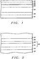
- the generic MTJ structure is schematically illustrated in FIG 1 . Seen there is bottom conductor 21, seed layer 22, AFM pinning layer 23, pinned ferromagnetic layer 24, tunneling barrier layer 25, free ferromagnetic layer 26, and capping layer 27.
- the three most critical layers in the MTJ stack are (a) pinned layer, (b) tunneling barrier layer, and (c) free layer.
- the pinned layer is a synthetic antiferromagnetic trilayer (e.g. CoFe/Ru/CoFe) that serves to reduce the offset field applied to the free layer.
- the tunneling barrier layer most widely used at present is an aluminum oxide (AlOx) layer formed by first depositing a 7-12 ⁇ thick Al film, which is subsequently oxidized, in-situ, by various means.
- AlOx aluminum oxide
- the MTJ's free layer is best made of a thin permalloy (NiFe) film, selected for its reproducible and reliable switching characteristics --- low switching field (Hc) and good switching field uniformity (Hc).
- the intrinsic dR/R that is obtainable for a NiFe-MTJ is, at best, around 40% for a R.A value (resistance.area product) between 1,000 to 10,000 ohm- ⁇ m 2 .
- the MTJ during a read operation is biased at 300-400 mv. At this bias voltage, the effective dR/R is around 25%.
- MTJ bit size would be reduced to less than 0.2 x 0.4 ⁇ m 2 .
- MTJs made with a monocrystalline MgO barrier layer and a CoFe(B) free layer are capable of a very high dR/R of more than 200% (4-6).
- Such a huge dR/R is the result of coherent tunneling (7) in which the electron symmetry of the ferromagnetic electrode is preserved during tunneling through the crystalline MgO barrier.
- strongly 001 oriented MgO is formed on top of the crystalline oriented CoFe pinned layer (AP1).
- the MgO was formed by reactive sputtering of a Mg target in a Ar/O 2 gas mixture R.A for these MgO MTJs was greater than 10,000 ohm- ⁇ m 2 .
- the MgO-MTJ described in reference (6) is made in the Anelva C-7100 sputtering system.
- Highly oriented (001) MgO is also formed on top of an amorphous CoFeB pinned layer (AP1), a R.A of 460 ohm- ⁇ m 2 being reported.
- the specific structure was: Ta50/CuN200/Ta30/MP150/CoFe(30%)25/Ru8.5/CoFeB30/MgO18/FL/Capping (360°C-2hrs -10K Oe).
- the crystalline MgO tunnel barrier formed by RF-sputtering from an MgO target, does not match well with the NiFe free layer.
- Patent 6,347,049 (Childress et al ) describes a trilayer tunneling barrier of MgO/AIO/MgO.
- the Mg and Al are deposited and oxidized, then the second layer of Mg is deposited and oxidized.
- McEvoy C et al "Proximity influence of a ferromagnet on the magnetoresistance of Cr film across a nonmagnetic layer" JOURNAL OF MAGNETISM AND MAGNETIC MATERIALS, ELSEVIER SCIENCE PUBLISHERS, AMSTERDAM, NL, vol. 283, no.
- Patent WO2006/094821 A2 discloses a method for producing thin magnesium oxide layers on a substrate.
- WONG P K ET AL "High conductance magnetoresistive tunnel junctions with multiply oxidized barrier" JOURNAL OF APPLIED PHYSICS, vol. 83, no.11, 1 June 1998 (1998-06-01), pages 6697-6699, XP012044143ISSN: 0021-8979 discloses 8x8 ⁇ m 2 mesa junctions fabricated from ultrahigh vacuum magnetron sputter-deposited Nb/Fe/Al 2 O 3 /Al/CoFe/Nb heterostructures.
- Patent US6219274 B1 discloses a ferromagnetic tunnel magnetoresistance effect element having a multilayered structure comprising a tunnel barrier layer and a first and a second ferromagnetic layer formed to sandwich the tunnel barrier layer therebetween, wherein the tunnel barrier layer is formed as an oxide film obtained by oxidizing a non-magnetic metal layer according to a radical oxidation method.
- Patent DE10020769 A1 discloses a method of forming a tunnel barrier layer comprising sequentially depositing and oxidizing at least two metal layers.
- Patent US5764567 A discloses a magnetic tunnel junction device, usable as a memory cell or an external magnetic field sensor, has a tunneling magnetoresistance response, as a function of applied magnetic field, that is substantially symmetric about zero field.
- Patent application US2004/101978 A1 discloses a fabrication process for a tunneling magnetoresistance (TMR) sensor.
- TMR tunneling magnetoresistance
- Patent application US2002/114112 A1 discloses a magnetic tunnel element including a plurality of ferromagnetic films laminated across an insulating film formed of metal oxide films and in which asymmetric tunnel barriers are formed along the direction in which the ferromagnetic films are laminated by this insulating film.
- Patent application US 2002/0097534 A1 discloses a magnetic tunnel junction with a triple-layer, e.g. MgO/MgO/Mg, tunneling barrier in which the lower layers are fully oxidized, and the top layer is non-oxidized.
- Another object of at least one embodiment of the present invention has been to provide a process for forming said tunneling barrier layer.
- said MTJ element include a NiFe free layer in order to minimize magnetostriction (s), switching field Hc, and switching field uniformity Hc.
- a further object of at least one embodiment of the present invention has been that said MTJ structure have a dR/R greater than 60% together with an R.A value less than about 1,000 ohm. ⁇ m 2 and an interlayer coupling field (Hin) less than 4 Oe.
- a layer of magnesium is deposited by DC magnetron sputtering and converted to magnesium oxide through radical oxidation wherein oxygen is excited at a power level of between about 400 and 600 watts and then passed over said first magnesium layer.
- a second, thinner, magnesium layer that is converted to magnesium oxide through radical oxidation wherein oxygen is excited at a power level of between about 200 and 300 watts and then passed over said first magnesium layer.
- a third magnesium layer that need not be oxidized.
- the MgO barrier layer is formed by first sputter depositing a Mg film to a certain thickness (typically between about 10 and 13 Angstroms), and then oxidizing it using a ROX (radical oxygen) process. This is followed by the deposition of a second (thinner) layer of magnesium (to a thickness between about 3 and 4 Angstroms) that is then oxidized using natural oxidation (NOX).
- FIG. 2 illustrates how the conventional barrier layer 25 of FIG. 1 has been replaced by ROX-formed layer 31 and NOX-formed layer 32.
- FIG. 3 shows a variation of FIG. 2 wherein bilayer 25 of FIG. 2 has been replaced by trilayer 35. The latter consists of the two magnesium oxide layers 31 and 32 plus an additional layer 33 of unoxidized magnesium.
- a critical feature of the present invention is that the magnesium layers are deposited by means of DC sputtering. It is important to distinguish this from RF - sputtering commonly used to deposit from a (dielectric) MgO target. Our use of DC sputtering of a (metallic) Mg target results in a uniform Mg film, which is particulate free.
- the ROX process used by the present invention involves placing a grid-like 'shower cap' between an upper ionizing electrode and the substrate (in this case Mg) inside an oxidation chamber.
- a shower of oxygen radicals is generated by said upper electrode through the application of 200-600 watts of RF power to oxygen flowing by at a rate of 0.2 to 0.5 SLM for a period of about 80 to 150 seconds.
- the first magnesium layer is oxidized by a first radical oxidation, wherein oxygen is excited by using an upper electrode, that flows over it at between about 0.3 and 0.5 SLM, at a power level of between about 400 and 600 watts and then passed over the first magnesium layer for between about 80 and 150 seconds, thereby forming the first layer of magnesium oxide 31.
- the second (thinner) magnesium layer is oxidized by a second radical oxidation, wherein oxygen is excited by using an upper electrode, that flows over it at between about 0.2 and 0.3 SLM, at a power level of between about 200 and 300 watts and then passed over the first magnesium layer for between about 80 and 150 seconds, thereby forming the second layer of magnesium oxide 32.
- Annealing of the structure is done at 360 °C for about 2 hours in a 10 kOe oriented field.
- annealing of the prior art CoFeB/AlOx/NiFe-MTJ structure was done at 280°C so the thermal stability of the MgO-MTJ is much better than that of an AlOx-MTJ.
- the NOX process used as part of the comparative examples present invention was implemented with oxygen that was passed over the magnesium at a pressure of between about 0.1 and 1 torr at room temperature.
- the resulting oxide has somewhat less preferred orientation than the lower layer, being closer in structure to an amorphous layer.
- Our criterion for distinguishing one level of preferred orientation over another has been to compare the relative intensities of the 001 peaks that appear in their respective X-ray diffraction patterns.
- Crystalline MgO as displayed by HRTEM (high resolution transmission electron microscopy), is highly (001) oriented. An Mg13 film after oxidation becomes a 15 ⁇ thick MgO layer. See TABLE II. dR/R of the CoFeB/Mg(11-13)/ROX/NiFe(21%)MTJ is greater than 60% and dR/R of the CoFeB/Mg(11-13)/ROX/NiFe(17.5%) MTJ is around 53%.
- dR/R of the 12 + 4 MTJ is around 62%.
- R.A is around 220 ohm- ⁇ m 2
- R.A is increased to 460 ohm- ⁇ m 2 but dR/R is slightly reduced.
- Hin is also increased. Over-all results shown in TABLE III indicate that increasing the top Mg thickness results in reducing dR/R.
- MgO/NiFe MTJs capable of delivering dR/R>60% for a NiFe17.5% MTJ structure, and dR/R>70% for a NiFe21%-MTJ structure.
- An R.A below 1,000 ohm- ⁇ m 2 and Hin ⁇ 1 Oe are also anticipated.
- Hc values for the NiFe(21%) free layer in the MgO-MTJ structure are smaller than for the AlOx-MTJ (2.2 Oe vs 2.4 Oe).
- CoFeB/MgO/NiFe MTJ structures formed according to the teachings of the present invention will be suitable for high density/high performance MRAM applications.
Landscapes
- Engineering & Computer Science (AREA)
- Chemical & Material Sciences (AREA)
- Nanotechnology (AREA)
- Crystallography & Structural Chemistry (AREA)
- Power Engineering (AREA)
- Manufacturing & Machinery (AREA)
- Physics & Mathematics (AREA)
- Chemical Kinetics & Catalysis (AREA)
- Spectroscopy & Molecular Physics (AREA)
- Materials Engineering (AREA)
- Mechanical Engineering (AREA)
- Metallurgy (AREA)
- Organic Chemistry (AREA)
- Condensed Matter Physics & Semiconductors (AREA)
- General Physics & Mathematics (AREA)
- Hall/Mr Elements (AREA)
- Physical Vapour Deposition (AREA)
- Formation Of Insulating Films (AREA)
Claims (5)
- Un procédé pour former une couche barrière tunnel (35), comprenant :
le dépôt, au moyen d'une pulvérisation D.C., d'une première couche de magnésium à une première épaisseur et étant caractérisée par :l'oxydation complète de ladite première couche de magnésium au moyen d'une première oxydation radicale dans laquelle l'oxygène est excité en utilisant une électrode supérieure, s'écoulant sur elle entre 0.3 et 0.5 SLM, à un niveau de puissance compris entre 400 et 600 watts et ensuite passé sur ladite première couche de magnésium pendant une durée entre 80 et 150 secondes, formant ainsi une première couche d'oxyde de magnésium (31) ;le dépôt, sur ladite première couche d'oxyde de magnésium, d'une seconde couche de magnésium à une seconde épaisseur, dans laquelle la seconde épaisseur est moindre que la première épaisseur ;l'oxydation complète de ladite seconde couche de magnésium au moyen d'une seconde oxydation radicale dans laquelle l'oxygène est excité en utilisant une électrode supérieure, s'écoulant sur elle entre 0.3 et 0.5 SLM, à un niveau de puissance compris entre 200 et 300 watts et ensuite passé sur ladite première couche de magnésium pendant une durée entre 80 et 150 secondes, formant ainsi une seconde couche d'oxyde de magnésium (32) ;le dépôt, sur ladite seconde couche d'oxyde de magnésium, d'une troisième couche de magnésium (33) à une troisième épaisseur, achevant ainsi la formation de la couche barrière tunnel. - Le procédé décrit dans la revendication 1 dans lequel ladite première épaisseur est entre 10x10-10 et 13x10-10 mètres.
- Le procédé décrit dans la revendication 1 dans lequel ladite seconde épaisseur est comprise entre 3x10⁻¹⁰ et 5x10⁻¹⁰ mètres.
- Le procédé décrit dans la revendication 1 dans lequel ladite troisième épaisseur est comprise entre 3x10⁻¹⁰ et 5x10⁻¹⁰ mètres.
- Le procédé décrit dans la revendication 1 dans lequel ladite couche tunnel complété est libre de toute contamination de particule.
Applications Claiming Priority (1)
| Application Number | Priority Date | Filing Date | Title |
|---|---|---|---|
| US11/317,388 US7479394B2 (en) | 2005-12-22 | 2005-12-22 | MgO/NiFe MTJ for high performance MRAM application |
Publications (3)
| Publication Number | Publication Date |
|---|---|
| EP1801895A2 EP1801895A2 (fr) | 2007-06-27 |
| EP1801895A3 EP1801895A3 (fr) | 2011-01-12 |
| EP1801895B1 true EP1801895B1 (fr) | 2020-04-22 |
Family
ID=37806188
Family Applications (1)
| Application Number | Title | Priority Date | Filing Date |
|---|---|---|---|
| EP06392019.3A Active EP1801895B1 (fr) | 2005-12-22 | 2006-12-20 | MTJ MgO/NiFe pour application MRAM haute performance |
Country Status (3)
| Country | Link |
|---|---|
| US (1) | US7479394B2 (fr) |
| EP (1) | EP1801895B1 (fr) |
| JP (1) | JP5068989B2 (fr) |
Families Citing this family (50)
| Publication number | Priority date | Publication date | Assignee | Title |
|---|---|---|---|---|
| US7264974B2 (en) * | 2004-01-30 | 2007-09-04 | Headway Technologies, Inc. | Method for fabricating a low resistance TMR read head |
| US7780820B2 (en) * | 2005-11-16 | 2010-08-24 | Headway Technologies, Inc. | Low resistance tunneling magnetoresistive sensor with natural oxidized double MgO barrier |
| JP4876708B2 (ja) * | 2006-05-11 | 2012-02-15 | Tdk株式会社 | トンネル磁気抵抗効果素子の製造方法、薄膜磁気ヘッドの製造方法及び磁気メモリの製造方法 |
| JP2007305768A (ja) * | 2006-05-11 | 2007-11-22 | Tdk Corp | トンネル磁気抵抗効果素子の製造方法、薄膜磁気ヘッドの製造方法及び磁気メモリの製造方法 |
| US7595520B2 (en) * | 2006-07-31 | 2009-09-29 | Magic Technologies, Inc. | Capping layer for a magnetic tunnel junction device to enhance dR/R and a method of making the same |
| US7598579B2 (en) * | 2007-01-30 | 2009-10-06 | Magic Technologies, Inc. | Magnetic tunnel junction (MTJ) to reduce spin transfer magnetization switching current |
| US8372661B2 (en) * | 2007-10-31 | 2013-02-12 | Magic Technologies, Inc. | High performance MTJ element for conventional MRAM and for STT-RAM and a method for making the same |
| JP5062832B2 (ja) * | 2007-12-28 | 2012-10-31 | 富士通株式会社 | 磁気抵抗効果素子の製造方法 |
| JP5150284B2 (ja) * | 2008-01-30 | 2013-02-20 | 株式会社東芝 | 磁気抵抗効果素子およびその製造方法 |
| JP5361201B2 (ja) | 2008-01-30 | 2013-12-04 | 株式会社東芝 | 磁気抵抗効果素子の製造方法 |
| JP5351140B2 (ja) * | 2008-03-03 | 2013-11-27 | キヤノンアネルバ株式会社 | 磁気トンネル接合デバイスの製造方法 |
| US7948044B2 (en) * | 2008-04-09 | 2011-05-24 | Magic Technologies, Inc. | Low switching current MTJ element for ultra-high STT-RAM and a method for making the same |
| US8373948B2 (en) * | 2008-04-28 | 2013-02-12 | Hitachi Global Storage Technologies Netherlands B.V. | Tunnel magnetoresistance (TMR) structures with MGO barrier and methods of making same |
| US8138561B2 (en) * | 2008-09-18 | 2012-03-20 | Magic Technologies, Inc. | Structure and method to fabricate high performance MTJ devices for spin-transfer torque (STT)-RAM |
| US7880209B2 (en) * | 2008-10-09 | 2011-02-01 | Seagate Technology Llc | MRAM cells including coupled free ferromagnetic layers for stabilization |
| US8120126B2 (en) * | 2009-03-02 | 2012-02-21 | Qualcomm Incorporated | Magnetic tunnel junction device and fabrication |
| GB2483421B (en) | 2009-06-24 | 2013-10-09 | Canon Anelva Corp | Vacuum heating/cooling apparatus and manufacturing method of magnetoresistance element |
| US8381391B2 (en) * | 2009-06-26 | 2013-02-26 | Western Digital (Fremont), Llc | Method for providing a magnetic recording transducer |
| US8609262B2 (en) | 2009-07-17 | 2013-12-17 | Magic Technologies, Inc. | Structure and method to fabricate high performance MTJ devices for spin-transfer torque (STT)-RAM application |
| JP5596694B2 (ja) * | 2009-09-11 | 2014-09-24 | 株式会社アルバック | 薄膜形成方法 |
| US8184411B2 (en) * | 2009-10-26 | 2012-05-22 | Headway Technologies, Inc. | MTJ incorporating CoFe/Ni multilayer film with perpendicular magnetic anisotropy for MRAM application |
| CN102687297B (zh) | 2009-12-28 | 2014-12-24 | 佳能安内华股份有限公司 | 磁阻元件的制造方法 |
| US8692343B2 (en) * | 2010-04-26 | 2014-04-08 | Headway Technologies, Inc. | MR enhancing layer (MREL) for spintronic devices |
| US8953285B2 (en) | 2010-05-05 | 2015-02-10 | Headway Technologies, Inc. | Side shielded magnetoresistive (MR) read head with perpendicular magnetic free layer |
| US8920947B2 (en) | 2010-05-28 | 2014-12-30 | Headway Technologies, Inc. | Multilayer structure with high perpendicular anisotropy for device applications |
| US8470462B2 (en) * | 2010-11-30 | 2013-06-25 | Magic Technologies, Inc. | Structure and method for enhancing interfacial perpendicular anisotropy in CoFe(B)/MgO/CoFe(B) magnetic tunnel junctions |
| KR101487635B1 (ko) * | 2010-12-22 | 2015-01-29 | 가부시키가이샤 아루박 | 터널 자기 저항 소자의 제조 방법 |
| US8492169B2 (en) | 2011-08-15 | 2013-07-23 | Magic Technologies, Inc. | Magnetic tunnel junction for MRAM applications |
| EP2568305B1 (fr) * | 2011-09-09 | 2016-03-02 | Crocus Technology S.A. | Jonction de tunnel magnétique doté d'une barrière de tunnel améliorée |
| JP5998654B2 (ja) * | 2012-05-31 | 2016-09-28 | 東京エレクトロン株式会社 | 真空処理装置、真空処理方法及び記憶媒体 |
| US8921961B2 (en) * | 2012-09-14 | 2014-12-30 | Headway Technologies, Inc. | Storage element for STT MRAM applications |
| US9461242B2 (en) | 2013-09-13 | 2016-10-04 | Micron Technology, Inc. | Magnetic memory cells, methods of fabrication, semiconductor devices, memory systems, and electronic systems |
| US9608197B2 (en) | 2013-09-18 | 2017-03-28 | Micron Technology, Inc. | Memory cells, methods of fabrication, and semiconductor devices |
| TWI569484B (zh) * | 2014-01-24 | 2017-02-01 | 國立臺灣大學 | 具超晶格勢壘之磁穿隧接面及包含具超晶格勢壘磁穿隧接面之裝置 |
| US10454024B2 (en) | 2014-02-28 | 2019-10-22 | Micron Technology, Inc. | Memory cells, methods of fabrication, and memory devices |
| US9281466B2 (en) | 2014-04-09 | 2016-03-08 | Micron Technology, Inc. | Memory cells, semiconductor structures, semiconductor devices, and methods of fabrication |
| US9349945B2 (en) | 2014-10-16 | 2016-05-24 | Micron Technology, Inc. | Memory cells, semiconductor devices, and methods of fabrication |
| US9768377B2 (en) | 2014-12-02 | 2017-09-19 | Micron Technology, Inc. | Magnetic cell structures, and methods of fabrication |
| US10439131B2 (en) * | 2015-01-15 | 2019-10-08 | Micron Technology, Inc. | Methods of forming semiconductor devices including tunnel barrier materials |
| US9337415B1 (en) * | 2015-03-20 | 2016-05-10 | HGST Netherlands B.V. | Perpendicular spin transfer torque (STT) memory cell with double MgO interface and CoFeB layer for enhancement of perpendicular magnetic anisotropy |
| US9890449B2 (en) * | 2015-04-29 | 2018-02-13 | Seagate Technology Llc | Methods of forming MgO barrier layer |
| KR102465539B1 (ko) | 2015-09-18 | 2022-11-11 | 삼성전자주식회사 | 자기 터널 접합 구조체를 포함하는 반도체 소자 및 그의 형성 방법 |
| GB2548644B (en) | 2015-10-21 | 2020-09-02 | Canon Anelva Corp | Method for manufacturing magnetoresistive device |
| GB2561790B (en) * | 2016-02-01 | 2021-05-12 | Canon Anelva Corp | Manufacturing method of magneto-resistive effect device |
| KR102406277B1 (ko) | 2017-10-25 | 2022-06-08 | 삼성전자주식회사 | 자기 저항 메모리 소자 및 이의 제조 방법 |
| US11264557B2 (en) * | 2017-12-30 | 2022-03-01 | Integrated Silicon Solution, (Cayman) Inc. | High retention storage layer using ultra-low RA MgO process in perpendicular magnetic tunnel junctions for MRAM devices |
| KR102577238B1 (ko) | 2018-09-21 | 2023-09-12 | 삼성전자주식회사 | 반도체 소자 제조 방법 |
| CN112310277A (zh) * | 2019-07-31 | 2021-02-02 | 中电海康集团有限公司 | 磁隧道结的制备方法 |
| CN112750946B (zh) * | 2019-10-31 | 2023-06-02 | 上海磁宇信息科技有限公司 | 一种磁性随机存储器势垒层和自由层结构单元及其制备方法 |
| JP7417967B2 (ja) | 2020-12-25 | 2024-01-19 | ローレルバンクマシン株式会社 | 紙葉類処理装置 |
Citations (1)
| Publication number | Priority date | Publication date | Assignee | Title |
|---|---|---|---|---|
| US20020097534A1 (en) * | 2000-11-17 | 2002-07-25 | Tdk Corporation | Magnetic tunnel junction read head devices having a tunneling barrier formed by multi-layer, multi-oxidation processes |
Family Cites Families (15)
| Publication number | Priority date | Publication date | Assignee | Title |
|---|---|---|---|---|
| US5764567A (en) * | 1996-11-27 | 1998-06-09 | International Business Machines Corporation | Magnetic tunnel junction device with nonferromagnetic interface layer for improved magnetic field response |
| JP4614212B2 (ja) * | 1998-07-17 | 2011-01-19 | ヤマハ株式会社 | 磁気トンネル接合素子の製造方法 |
| JP3235572B2 (ja) * | 1998-09-18 | 2001-12-04 | 日本電気株式会社 | 磁気抵抗効果素子,磁気抵抗効果センサ及びそれらを利用したシステム |
| US6219274B1 (en) * | 1999-06-08 | 2001-04-17 | Tdk Corporation | Ferromagnetic tunnel magnetoresistance effect element and method of producing the same |
| JP3496215B2 (ja) * | 1999-06-16 | 2004-02-09 | 日本電気株式会社 | 強磁性トンネル接合素子の製造方法 |
| DE10020769C2 (de) * | 2000-04-28 | 2003-07-24 | Forschungszentrum Juelich Gmbh | Verfahren zum Herstellen magnetischer Tunnelkontakte |
| JP2002319722A (ja) * | 2001-01-22 | 2002-10-31 | Matsushita Electric Ind Co Ltd | 磁気抵抗効果素子とその製造方法 |
| JP2002314164A (ja) * | 2001-02-06 | 2002-10-25 | Sony Corp | 磁気トンネル素子及びその製造方法、薄膜磁気ヘッド、磁気メモリ、並びに磁気センサ |
| US6347049B1 (en) | 2001-07-25 | 2002-02-12 | International Business Machines Corporation | Low resistance magnetic tunnel junction device with bilayer or multilayer tunnel barrier |
| JP3906139B2 (ja) | 2002-10-16 | 2007-04-18 | 株式会社東芝 | 磁気ランダムアクセスメモリ |
| US6828260B2 (en) | 2002-10-29 | 2004-12-07 | Hewlett-Packard Development Company, L.P. | Ultra-violet treatment of a tunnel barrier layer through an overlayer a tunnel junction device |
| US6841395B2 (en) | 2002-11-25 | 2005-01-11 | International Business Machines Corporation | Method of forming a barrier layer of a tunneling magnetoresistive sensor |
| JP4082711B2 (ja) * | 2004-03-12 | 2008-04-30 | 独立行政法人科学技術振興機構 | 磁気抵抗素子及びその製造方法 |
| DE102005011414A1 (de) * | 2005-03-11 | 2006-09-14 | Singulus Technologies Ag | Verfahren zum Herstellen einer dünnen Magnesiumoxidschicht mittels Plasma-Oxidation |
| US7780820B2 (en) * | 2005-11-16 | 2010-08-24 | Headway Technologies, Inc. | Low resistance tunneling magnetoresistive sensor with natural oxidized double MgO barrier |
-
2005
- 2005-12-22 US US11/317,388 patent/US7479394B2/en active Active
-
2006
- 2006-12-20 EP EP06392019.3A patent/EP1801895B1/fr active Active
- 2006-12-22 JP JP2006346048A patent/JP5068989B2/ja active Active
Patent Citations (1)
| Publication number | Priority date | Publication date | Assignee | Title |
|---|---|---|---|---|
| US20020097534A1 (en) * | 2000-11-17 | 2002-07-25 | Tdk Corporation | Magnetic tunnel junction read head devices having a tunneling barrier formed by multi-layer, multi-oxidation processes |
Non-Patent Citations (1)
| Title |
|---|
| ZHU J G ( ET AL: "Magnetic tunnel junctions", MATERIALS TODAY, ELSEVIER SCIENCE, KIDLINGTON, GB, vol. 9, no. 11, 1 November 2006 (2006-11-01), pages 36 - 45, XP028034143, ISSN: 1369-7021, [retrieved on 20061101], DOI: 10.1016/S1369-7021(06)71693-5 * |
Also Published As
| Publication number | Publication date |
|---|---|
| JP2007173843A (ja) | 2007-07-05 |
| EP1801895A3 (fr) | 2011-01-12 |
| JP5068989B2 (ja) | 2012-11-07 |
| US20070148786A1 (en) | 2007-06-28 |
| EP1801895A2 (fr) | 2007-06-27 |
| US7479394B2 (en) | 2009-01-20 |
Similar Documents
| Publication | Publication Date | Title |
|---|---|---|
| EP1801895B1 (fr) | MTJ MgO/NiFe pour application MRAM haute performance | |
| USRE50331E1 (en) | Magnetoresistive stack and method of fabricating same | |
| US7045841B2 (en) | Oxidation structure/method to fabricate a high-performance magnetic tunneling junction MRAM | |
| EP3467891B1 (fr) | Réduction de produit de résistance de barrière x surface (ra) et protection des anisotropies mangnétiques pour des applications de dispositifs magnétiques perpendiculaires | |
| US7276384B2 (en) | Magnetic tunnel junctions with improved tunneling magneto-resistance | |
| US8823118B2 (en) | Spin torque transfer magnetic tunnel junction fabricated with a composite tunneling barrier layer | |
| US6831312B2 (en) | Amorphous alloys for magnetic devices | |
| EP2502232B1 (fr) | Jtm incorporant un film multicouche de cofe/ni avec anisotropie magnétique perpendiculaire pour application de mémoire vive magnétique | |
| EP2943957B1 (fr) | Couche d'insertion discontinue de magnésium (mg) permettant d'améliorer un shunt mtj | |
| US7777261B2 (en) | Magnetic device having stabilized free ferromagnetic layer | |
| KR100900109B1 (ko) | 자기저항 효과 소자 및 자기저항 랜덤 액세스 메모리 | |
| EP1885006B1 (fr) | Nouvelle couche d'encapsulage pour dispositif de jonction à effet tunnel magnétique pour améliorer la magnétorésistance dR/R et son procédé de fabrication | |
| US20070063237A1 (en) | Magnetic device having multilayered free ferromagnetic layer | |
| EP2705518A1 (fr) | Couches multiples ayant un champ de démagnétisation perpendiculaire réduit en utilisant un moment de dilution pour des applications spintroniques | |
| US7217577B2 (en) | Structure/method to fabricate a high-performance magnetic tunneling junction MRAM | |
| US11081154B1 (en) | Synthetic magnetic pinning element having strong antiferromagnetic coupling |
Legal Events
| Date | Code | Title | Description |
|---|---|---|---|
| PUAI | Public reference made under article 153(3) epc to a published international application that has entered the european phase |
Free format text: ORIGINAL CODE: 0009012 |
|
| AK | Designated contracting states |
Kind code of ref document: A2 Designated state(s): AT BE BG CH CY CZ DE DK EE ES FI FR GB GR HU IE IS IT LI LT LU LV MC NL PL PT RO SE SI SK TR |
|
| AX | Request for extension of the european patent |
Extension state: AL BA HR MK YU |
|
| RIC1 | Information provided on ipc code assigned before grant |
Ipc: G11C 11/16 20060101ALN20100729BHEP Ipc: H01F 41/18 20060101ALN20100729BHEP Ipc: C23C 14/58 20060101ALI20100729BHEP Ipc: H01F 41/30 20060101ALI20100729BHEP Ipc: H01F 10/32 20060101ALI20100729BHEP Ipc: H01L 43/12 20060101AFI20100729BHEP |
|
| PUAL | Search report despatched |
Free format text: ORIGINAL CODE: 0009013 |
|
| AK | Designated contracting states |
Kind code of ref document: A3 Designated state(s): AT BE BG CH CY CZ DE DK EE ES FI FR GB GR HU IE IS IT LI LT LU LV MC NL PL PT RO SE SI SK TR |
|
| AX | Request for extension of the european patent |
Extension state: AL BA HR MK RS |
|
| 17P | Request for examination filed |
Effective date: 20110712 |
|
| AKX | Designation fees paid |
Designated state(s): AT BE BG CH CY CZ DE DK EE ES FI FR GB GR HU IE IS IT LI LT LU LV MC NL PL PT RO SE SI SK TR |
|
| 17Q | First examination report despatched |
Effective date: 20140502 |
|
| RAP1 | Party data changed (applicant data changed or rights of an application transferred) |
Owner name: HEADWAY TECHNOLOGIES, INC. |
|
| STAA | Information on the status of an ep patent application or granted ep patent |
Free format text: STATUS: EXAMINATION IS IN PROGRESS |
|
| REG | Reference to a national code |
Ref country code: DE Ref legal event code: R079 Ref document number: 602006059338 Country of ref document: DE Free format text: PREVIOUS MAIN CLASS: H01L0043000000 Ipc: H01L0043120000 |
|
| GRAP | Despatch of communication of intention to grant a patent |
Free format text: ORIGINAL CODE: EPIDOSNIGR1 |
|
| STAA | Information on the status of an ep patent application or granted ep patent |
Free format text: STATUS: GRANT OF PATENT IS INTENDED |
|
| RIC1 | Information provided on ipc code assigned before grant |
Ipc: H01F 41/18 20060101ALN20191021BHEP Ipc: H01L 43/12 20060101AFI20191021BHEP Ipc: H01F 10/32 20060101ALI20191021BHEP Ipc: C23C 14/58 20060101ALI20191021BHEP Ipc: G11C 11/16 20060101ALN20191021BHEP Ipc: H01F 41/30 20060101ALI20191021BHEP |
|
| RIC1 | Information provided on ipc code assigned before grant |
Ipc: C23C 14/58 20060101ALI20191025BHEP Ipc: G11C 11/16 20060101ALN20191025BHEP Ipc: H01F 10/32 20060101ALI20191025BHEP Ipc: H01F 41/30 20060101ALI20191025BHEP Ipc: H01F 41/18 20060101ALN20191025BHEP Ipc: H01L 43/12 20060101AFI20191025BHEP |
|
| INTG | Intention to grant announced |
Effective date: 20191113 |
|
| GRAS | Grant fee paid |
Free format text: ORIGINAL CODE: EPIDOSNIGR3 |
|
| GRAA | (expected) grant |
Free format text: ORIGINAL CODE: 0009210 |
|
| STAA | Information on the status of an ep patent application or granted ep patent |
Free format text: STATUS: THE PATENT HAS BEEN GRANTED |
|
| REG | Reference to a national code |
Ref country code: DE Ref legal event code: R081 Ref document number: 602006059338 Country of ref document: DE Owner name: TAIWAN SEMICONDUCTOR MANUFACTURING COMPANY, LT, TW Free format text: FORMER OWNER: MAGIC TECHNOLOGIES, INC., MILPITAS, CALIF., US |
|
| AK | Designated contracting states |
Kind code of ref document: B1 Designated state(s): AT BE BG CH CY CZ DE DK EE ES FI FR GB GR HU IE IS IT LI LT LU LV MC NL PL PT RO SE SI SK TR |
|
| REG | Reference to a national code |
Ref country code: GB Ref legal event code: FG4D |
|
| REG | Reference to a national code |
Ref country code: CH Ref legal event code: EP |
|
| REG | Reference to a national code |
Ref country code: DE Ref legal event code: R096 Ref document number: 602006059338 Country of ref document: DE |
|
| REG | Reference to a national code |
Ref country code: IE Ref legal event code: FG4D |
|
| REG | Reference to a national code |
Ref country code: AT Ref legal event code: REF Ref document number: 1261308 Country of ref document: AT Kind code of ref document: T Effective date: 20200515 |
|
| REG | Reference to a national code |
Ref country code: LT Ref legal event code: MG4D |
|
| REG | Reference to a national code |
Ref country code: NL Ref legal event code: MP Effective date: 20200422 |
|
| PG25 | Lapsed in a contracting state [announced via postgrant information from national office to epo] |
Ref country code: GR Free format text: LAPSE BECAUSE OF FAILURE TO SUBMIT A TRANSLATION OF THE DESCRIPTION OR TO PAY THE FEE WITHIN THE PRESCRIBED TIME-LIMIT Effective date: 20200723 Ref country code: SE Free format text: LAPSE BECAUSE OF FAILURE TO SUBMIT A TRANSLATION OF THE DESCRIPTION OR TO PAY THE FEE WITHIN THE PRESCRIBED TIME-LIMIT Effective date: 20200422 Ref country code: IS Free format text: LAPSE BECAUSE OF FAILURE TO SUBMIT A TRANSLATION OF THE DESCRIPTION OR TO PAY THE FEE WITHIN THE PRESCRIBED TIME-LIMIT Effective date: 20200822 Ref country code: FI Free format text: LAPSE BECAUSE OF FAILURE TO SUBMIT A TRANSLATION OF THE DESCRIPTION OR TO PAY THE FEE WITHIN THE PRESCRIBED TIME-LIMIT Effective date: 20200422 Ref country code: LT Free format text: LAPSE BECAUSE OF FAILURE TO SUBMIT A TRANSLATION OF THE DESCRIPTION OR TO PAY THE FEE WITHIN THE PRESCRIBED TIME-LIMIT Effective date: 20200422 Ref country code: NL Free format text: LAPSE BECAUSE OF FAILURE TO SUBMIT A TRANSLATION OF THE DESCRIPTION OR TO PAY THE FEE WITHIN THE PRESCRIBED TIME-LIMIT Effective date: 20200422 Ref country code: PT Free format text: LAPSE BECAUSE OF FAILURE TO SUBMIT A TRANSLATION OF THE DESCRIPTION OR TO PAY THE FEE WITHIN THE PRESCRIBED TIME-LIMIT Effective date: 20200824 |
|
| REG | Reference to a national code |
Ref country code: AT Ref legal event code: MK05 Ref document number: 1261308 Country of ref document: AT Kind code of ref document: T Effective date: 20200422 |
|
| PG25 | Lapsed in a contracting state [announced via postgrant information from national office to epo] |
Ref country code: LV Free format text: LAPSE BECAUSE OF FAILURE TO SUBMIT A TRANSLATION OF THE DESCRIPTION OR TO PAY THE FEE WITHIN THE PRESCRIBED TIME-LIMIT Effective date: 20200422 Ref country code: BG Free format text: LAPSE BECAUSE OF FAILURE TO SUBMIT A TRANSLATION OF THE DESCRIPTION OR TO PAY THE FEE WITHIN THE PRESCRIBED TIME-LIMIT Effective date: 20200722 |
|
| REG | Reference to a national code |
Ref country code: DE Ref legal event code: R097 Ref document number: 602006059338 Country of ref document: DE |
|
| PG25 | Lapsed in a contracting state [announced via postgrant information from national office to epo] |
Ref country code: IT Free format text: LAPSE BECAUSE OF FAILURE TO SUBMIT A TRANSLATION OF THE DESCRIPTION OR TO PAY THE FEE WITHIN THE PRESCRIBED TIME-LIMIT Effective date: 20200422 Ref country code: CZ Free format text: LAPSE BECAUSE OF FAILURE TO SUBMIT A TRANSLATION OF THE DESCRIPTION OR TO PAY THE FEE WITHIN THE PRESCRIBED TIME-LIMIT Effective date: 20200422 Ref country code: RO Free format text: LAPSE BECAUSE OF FAILURE TO SUBMIT A TRANSLATION OF THE DESCRIPTION OR TO PAY THE FEE WITHIN THE PRESCRIBED TIME-LIMIT Effective date: 20200422 Ref country code: ES Free format text: LAPSE BECAUSE OF FAILURE TO SUBMIT A TRANSLATION OF THE DESCRIPTION OR TO PAY THE FEE WITHIN THE PRESCRIBED TIME-LIMIT Effective date: 20200422 Ref country code: DK Free format text: LAPSE BECAUSE OF FAILURE TO SUBMIT A TRANSLATION OF THE DESCRIPTION OR TO PAY THE FEE WITHIN THE PRESCRIBED TIME-LIMIT Effective date: 20200422 Ref country code: AT Free format text: LAPSE BECAUSE OF FAILURE TO SUBMIT A TRANSLATION OF THE DESCRIPTION OR TO PAY THE FEE WITHIN THE PRESCRIBED TIME-LIMIT Effective date: 20200422 Ref country code: EE Free format text: LAPSE BECAUSE OF FAILURE TO SUBMIT A TRANSLATION OF THE DESCRIPTION OR TO PAY THE FEE WITHIN THE PRESCRIBED TIME-LIMIT Effective date: 20200422 |
|
| REG | Reference to a national code |
Ref country code: DE Ref legal event code: R081 Ref document number: 602006059338 Country of ref document: DE Owner name: TAIWAN SEMICONDUCTOR MANUFACTURING COMPANY, LT, TW Free format text: FORMER OWNER: HEADWAY TECHNOLOGIES, INC., MILPITAS, CALIF., US |
|
| PG25 | Lapsed in a contracting state [announced via postgrant information from national office to epo] |
Ref country code: SK Free format text: LAPSE BECAUSE OF FAILURE TO SUBMIT A TRANSLATION OF THE DESCRIPTION OR TO PAY THE FEE WITHIN THE PRESCRIBED TIME-LIMIT Effective date: 20200422 Ref country code: PL Free format text: LAPSE BECAUSE OF FAILURE TO SUBMIT A TRANSLATION OF THE DESCRIPTION OR TO PAY THE FEE WITHIN THE PRESCRIBED TIME-LIMIT Effective date: 20200422 |
|
| PLBE | No opposition filed within time limit |
Free format text: ORIGINAL CODE: 0009261 |
|
| STAA | Information on the status of an ep patent application or granted ep patent |
Free format text: STATUS: NO OPPOSITION FILED WITHIN TIME LIMIT |
|
| 26N | No opposition filed |
Effective date: 20210125 |
|
| PG25 | Lapsed in a contracting state [announced via postgrant information from national office to epo] |
Ref country code: SI Free format text: LAPSE BECAUSE OF FAILURE TO SUBMIT A TRANSLATION OF THE DESCRIPTION OR TO PAY THE FEE WITHIN THE PRESCRIBED TIME-LIMIT Effective date: 20200422 |
|
| REG | Reference to a national code |
Ref country code: CH Ref legal event code: PL |
|
| GBPC | Gb: european patent ceased through non-payment of renewal fee |
Effective date: 20201220 |
|
| PG25 | Lapsed in a contracting state [announced via postgrant information from national office to epo] |
Ref country code: MC Free format text: LAPSE BECAUSE OF FAILURE TO SUBMIT A TRANSLATION OF THE DESCRIPTION OR TO PAY THE FEE WITHIN THE PRESCRIBED TIME-LIMIT Effective date: 20200422 |
|
| REG | Reference to a national code |
Ref country code: BE Ref legal event code: MM Effective date: 20201231 |
|
| PG25 | Lapsed in a contracting state [announced via postgrant information from national office to epo] |
Ref country code: IE Free format text: LAPSE BECAUSE OF NON-PAYMENT OF DUE FEES Effective date: 20201220 Ref country code: LU Free format text: LAPSE BECAUSE OF NON-PAYMENT OF DUE FEES Effective date: 20201220 Ref country code: FR Free format text: LAPSE BECAUSE OF NON-PAYMENT OF DUE FEES Effective date: 20201231 |
|
| PG25 | Lapsed in a contracting state [announced via postgrant information from national office to epo] |
Ref country code: GB Free format text: LAPSE BECAUSE OF NON-PAYMENT OF DUE FEES Effective date: 20201220 Ref country code: CH Free format text: LAPSE BECAUSE OF NON-PAYMENT OF DUE FEES Effective date: 20201231 Ref country code: LI Free format text: LAPSE BECAUSE OF NON-PAYMENT OF DUE FEES Effective date: 20201231 |
|
| PG25 | Lapsed in a contracting state [announced via postgrant information from national office to epo] |
Ref country code: TR Free format text: LAPSE BECAUSE OF FAILURE TO SUBMIT A TRANSLATION OF THE DESCRIPTION OR TO PAY THE FEE WITHIN THE PRESCRIBED TIME-LIMIT Effective date: 20200422 Ref country code: CY Free format text: LAPSE BECAUSE OF FAILURE TO SUBMIT A TRANSLATION OF THE DESCRIPTION OR TO PAY THE FEE WITHIN THE PRESCRIBED TIME-LIMIT Effective date: 20200422 |
|
| PG25 | Lapsed in a contracting state [announced via postgrant information from national office to epo] |
Ref country code: BE Free format text: LAPSE BECAUSE OF NON-PAYMENT OF DUE FEES Effective date: 20201231 |
|
| REG | Reference to a national code |
Ref country code: DE Ref legal event code: R079 Ref document number: 602006059338 Country of ref document: DE Free format text: PREVIOUS MAIN CLASS: H01L0043120000 Ipc: H10N0050010000 |
|
| PG25 | Lapsed in a contracting state [announced via postgrant information from national office to epo] |
Ref country code: IS Free format text: LAPSE BECAUSE OF NON-PAYMENT OF DUE FEES Effective date: 20200822 |
|
| PGFP | Annual fee paid to national office [announced via postgrant information from national office to epo] |
Ref country code: DE Payment date: 20251229 Year of fee payment: 20 |