EP1803836A1 - Source d'évaporation et procédé de dépôt de couches minces l'utilisant - Google Patents
Source d'évaporation et procédé de dépôt de couches minces l'utilisant Download PDFInfo
- Publication number
- EP1803836A1 EP1803836A1 EP06256598A EP06256598A EP1803836A1 EP 1803836 A1 EP1803836 A1 EP 1803836A1 EP 06256598 A EP06256598 A EP 06256598A EP 06256598 A EP06256598 A EP 06256598A EP 1803836 A1 EP1803836 A1 EP 1803836A1
- Authority
- EP
- European Patent Office
- Prior art keywords
- evaporation source
- crucible
- deposition
- baffle
- deposition material
- Prior art date
- Legal status (The legal status is an assumption and is not a legal conclusion. Google has not performed a legal analysis and makes no representation as to the accuracy of the status listed.)
- Granted
Links
Images

Classifications
-
- C—CHEMISTRY; METALLURGY
- C23—COATING METALLIC MATERIAL; COATING MATERIAL WITH METALLIC MATERIAL; CHEMICAL SURFACE TREATMENT; DIFFUSION TREATMENT OF METALLIC MATERIAL; COATING BY VACUUM EVAPORATION, BY SPUTTERING, BY ION IMPLANTATION OR BY CHEMICAL VAPOUR DEPOSITION, IN GENERAL; INHIBITING CORROSION OF METALLIC MATERIAL OR INCRUSTATION IN GENERAL
- C23C—COATING METALLIC MATERIAL; COATING MATERIAL WITH METALLIC MATERIAL; SURFACE TREATMENT OF METALLIC MATERIAL BY DIFFUSION INTO THE SURFACE, BY CHEMICAL CONVERSION OR SUBSTITUTION; COATING BY VACUUM EVAPORATION, BY SPUTTERING, BY ION IMPLANTATION OR BY CHEMICAL VAPOUR DEPOSITION, IN GENERAL
- C23C14/00—Coating by vacuum evaporation, by sputtering or by ion implantation of the coating forming material
- C23C14/06—Coating by vacuum evaporation, by sputtering or by ion implantation of the coating forming material characterised by the coating material
- C23C14/12—Organic material
-
- C—CHEMISTRY; METALLURGY
- C23—COATING METALLIC MATERIAL; COATING MATERIAL WITH METALLIC MATERIAL; CHEMICAL SURFACE TREATMENT; DIFFUSION TREATMENT OF METALLIC MATERIAL; COATING BY VACUUM EVAPORATION, BY SPUTTERING, BY ION IMPLANTATION OR BY CHEMICAL VAPOUR DEPOSITION, IN GENERAL; INHIBITING CORROSION OF METALLIC MATERIAL OR INCRUSTATION IN GENERAL
- C23C—COATING METALLIC MATERIAL; COATING MATERIAL WITH METALLIC MATERIAL; SURFACE TREATMENT OF METALLIC MATERIAL BY DIFFUSION INTO THE SURFACE, BY CHEMICAL CONVERSION OR SUBSTITUTION; COATING BY VACUUM EVAPORATION, BY SPUTTERING, BY ION IMPLANTATION OR BY CHEMICAL VAPOUR DEPOSITION, IN GENERAL
- C23C14/00—Coating by vacuum evaporation, by sputtering or by ion implantation of the coating forming material
- C23C14/22—Coating by vacuum evaporation, by sputtering or by ion implantation of the coating forming material characterised by the process of coating
- C23C14/24—Vacuum evaporation
- C23C14/243—Crucibles for source material
-
- C—CHEMISTRY; METALLURGY
- C23—COATING METALLIC MATERIAL; COATING MATERIAL WITH METALLIC MATERIAL; CHEMICAL SURFACE TREATMENT; DIFFUSION TREATMENT OF METALLIC MATERIAL; COATING BY VACUUM EVAPORATION, BY SPUTTERING, BY ION IMPLANTATION OR BY CHEMICAL VAPOUR DEPOSITION, IN GENERAL; INHIBITING CORROSION OF METALLIC MATERIAL OR INCRUSTATION IN GENERAL
- C23C—COATING METALLIC MATERIAL; COATING MATERIAL WITH METALLIC MATERIAL; SURFACE TREATMENT OF METALLIC MATERIAL BY DIFFUSION INTO THE SURFACE, BY CHEMICAL CONVERSION OR SUBSTITUTION; COATING BY VACUUM EVAPORATION, BY SPUTTERING, BY ION IMPLANTATION OR BY CHEMICAL VAPOUR DEPOSITION, IN GENERAL
- C23C14/00—Coating by vacuum evaporation, by sputtering or by ion implantation of the coating forming material
- C23C14/22—Coating by vacuum evaporation, by sputtering or by ion implantation of the coating forming material characterised by the process of coating
- C23C14/24—Vacuum evaporation
- C23C14/246—Replenishment of source material
-
- C—CHEMISTRY; METALLURGY
- C23—COATING METALLIC MATERIAL; COATING MATERIAL WITH METALLIC MATERIAL; CHEMICAL SURFACE TREATMENT; DIFFUSION TREATMENT OF METALLIC MATERIAL; COATING BY VACUUM EVAPORATION, BY SPUTTERING, BY ION IMPLANTATION OR BY CHEMICAL VAPOUR DEPOSITION, IN GENERAL; INHIBITING CORROSION OF METALLIC MATERIAL OR INCRUSTATION IN GENERAL
- C23C—COATING METALLIC MATERIAL; COATING MATERIAL WITH METALLIC MATERIAL; SURFACE TREATMENT OF METALLIC MATERIAL BY DIFFUSION INTO THE SURFACE, BY CHEMICAL CONVERSION OR SUBSTITUTION; COATING BY VACUUM EVAPORATION, BY SPUTTERING, BY ION IMPLANTATION OR BY CHEMICAL VAPOUR DEPOSITION, IN GENERAL
- C23C14/00—Coating by vacuum evaporation, by sputtering or by ion implantation of the coating forming material
- C23C14/22—Coating by vacuum evaporation, by sputtering or by ion implantation of the coating forming material characterised by the process of coating
- C23C14/24—Vacuum evaporation
- C23C14/26—Vacuum evaporation by resistance or inductive heating of the source
-
- C—CHEMISTRY; METALLURGY
- C23—COATING METALLIC MATERIAL; COATING MATERIAL WITH METALLIC MATERIAL; CHEMICAL SURFACE TREATMENT; DIFFUSION TREATMENT OF METALLIC MATERIAL; COATING BY VACUUM EVAPORATION, BY SPUTTERING, BY ION IMPLANTATION OR BY CHEMICAL VAPOUR DEPOSITION, IN GENERAL; INHIBITING CORROSION OF METALLIC MATERIAL OR INCRUSTATION IN GENERAL
- C23C—COATING METALLIC MATERIAL; COATING MATERIAL WITH METALLIC MATERIAL; SURFACE TREATMENT OF METALLIC MATERIAL BY DIFFUSION INTO THE SURFACE, BY CHEMICAL CONVERSION OR SUBSTITUTION; COATING BY VACUUM EVAPORATION, BY SPUTTERING, BY ION IMPLANTATION OR BY CHEMICAL VAPOUR DEPOSITION, IN GENERAL
- C23C14/00—Coating by vacuum evaporation, by sputtering or by ion implantation of the coating forming material
- C23C14/22—Coating by vacuum evaporation, by sputtering or by ion implantation of the coating forming material characterised by the process of coating
- C23C14/34—Sputtering
-
- C—CHEMISTRY; METALLURGY
- C23—COATING METALLIC MATERIAL; COATING MATERIAL WITH METALLIC MATERIAL; CHEMICAL SURFACE TREATMENT; DIFFUSION TREATMENT OF METALLIC MATERIAL; COATING BY VACUUM EVAPORATION, BY SPUTTERING, BY ION IMPLANTATION OR BY CHEMICAL VAPOUR DEPOSITION, IN GENERAL; INHIBITING CORROSION OF METALLIC MATERIAL OR INCRUSTATION IN GENERAL
- C23C—COATING METALLIC MATERIAL; COATING MATERIAL WITH METALLIC MATERIAL; SURFACE TREATMENT OF METALLIC MATERIAL BY DIFFUSION INTO THE SURFACE, BY CHEMICAL CONVERSION OR SUBSTITUTION; COATING BY VACUUM EVAPORATION, BY SPUTTERING, BY ION IMPLANTATION OR BY CHEMICAL VAPOUR DEPOSITION, IN GENERAL
- C23C16/00—Chemical coating by decomposition of gaseous compounds, without leaving reaction products of surface material in the coating, i.e. chemical vapour deposition [CVD] processes
-
- H01L21/203—
Definitions
- the present invention relates to an evaporation source and a method for depositing thin films using the same.
- the present invention relates to an evaporation source and method for depositing thin films capable of providing uniform film thickness and minimized heat radiation.
- thin films may be deposited in display devices, such as electroluminescent (EL) display devices, to provide photon-emitting mediums to form images.
- EL electroluminescent
- Such thin films may be applied to a substrate, e.g., an electrode, by methods such as physical vapor deposition (PVD), e.g., vacuum deposition, chemical vapor deposition (CVD), ion plating, sputtering, and so forth.
- PVD physical vapor deposition
- CVD chemical vapor deposition
- ion plating ion plating
- sputtering ion plating
- sputtering e.g., a substrate
- a vacuum environment e.g., vacuum chamber
- An evaporation source having a heating unit and a deposition material e.g., organic light-emitting material, may be either connected to the vacuum environment or installed therein, such that the operation of the evaporation source may evaporate the deposition material and form a thin film on the substrate.
- An evaporation source may include a crucible to contain a deposition material, a heating unit to heat the crucible and evaporate the deposition material, and at least one spray nozzle to apply the evaporated deposition material to a substrate.
- the particles of the evaporated deposition material may have a tendency to coalesce and form clusters of particles having various sizes, thereby providing an evaporated deposition material having non-uniform texture and density consistency. Further, such non-uniform evaporated deposition material may cause application of non-uniform layers of deposition material onto substrates, thereby producing films lacking uniform thickness.
- application of the evaporated deposition material through a conventional spray nozzle onto a substrate may radiate excess heat into a processing chamber, thereby deforming the substrate upon contact therewith.
- deposition material to a rotatable substrate may require a large size of a processing chamber in order to accommodate sufficient space for substrate movement. Such large substrates may also sag or collapse as a result of upward application of deposition material thereon.
- the present invention is therefore directed to an evaporation source and method of employing the same, which substantially overcome one or more of the disadvantages of the related art.
- the invention accordingly sets out to provide an evaporation source and a method employing the same having the capability of minimizing the coalescence of the evaporated deposition material, thereby improving uniformity of thin deposition layers.
- the invention also aims to provide an evaporation source and a method employing the same having a nozzle structure with improved heat radiation distribution, thereby minimizing excessive heat transfer into a processing chamber.
- a first aspect of the invention provides an evaporation source as set out in claim 1.
- Preferred features of this aspect of the invention are set out in claims 2 to 10.
- a second aspect of the invention provdes a method of depositing a thin film as set out in Claim 11. Preferred features of this aspect of the invention are set out in claims 12 to 16.
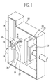
- FIG. 1 illustrates a perspective view of an apparatus for depositing a thin films using an evaporation source according to an embodiment of the present invention
- FIG. 2A illustrates a cross-sectional view of an evaporation source according to an embodiment of the present invention taken along the line I-I' of FIG. 1;
- FIG. 2B illustrates a cross-sectional view of a direction of movement of an evaporated deposition material inside an evaporation source according to an embodiment of the present invention taken along the line I-I' of FIG. 1;
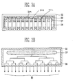
- FIG. 3A illustrates a plan view of an evaporation source according to an embodiment of the present invention taken along the line II-II' of FIG. 1;
- FIG. 3B illustrates a plan view of a direction of movement of an evaporated deposition material inside an evaporation source having a shower head structure according to an embodiment of the present invention taken along the line II-II' of FIG. 1.
- an apparatus for depositing thin films includes a processing chamber 20, a supporting unit 23 for securing a substrate, an evaporation source 24, and a deposition rate measuring unit 26 coupled to the evaporation source 24.
- the processing chamber 20 of an embodiment of the present invention may be any type of vessel known by those skilled in the art for use in film processing, and, preferably, it may be a pressure-controlled vessel such as a vacuum chamber.
- the processing chamber 20 is in this case formed to have a deposition preventing part A and a film forming part B.
- the film forming part B refers to the central area of the processing chamber 20.
- the central area of the processing chamber 20 corresponds to a position where a substrate may be placed and formation of a film, e.g., vacuum deposition processing, may occur.
- the deposition preventing part A refers to the area inside the processing chamber 20 that surrounds the film forming part B. In other words, the deposition preventing part A is formed as peripheral portions of film forming part B.
- the peripheral portions, i.e., deposition preventing part A are excluded from film deposition processing.
- the deposition preventing part A may include a heat absorbing plate (not shown) formed around a substrate to remove excess heat from the substrate and provide uniform temperature and uniform film thickness.
- a substrate 21 and a mask 22 are in use, placed in the processing chamber 20.
- the substrate 21 and mask 22 are placed in the center of the processing chamber 20, i.e., film forming part B, such that the deposition preventing part A surrounds them.
- the mask 22 is attached to the substrate 21 between the substrate 21 and the evaporation source 24.
- the mask 22 may include a pattern formation unit (not shown) having a pattern corresponding to a pattern to be imparted to a thin film formed on the substrate 21, and a fixation unit (not shown) secured to a mask frame (not shown) through welding.
- the supporting unit 23 of this embodiment of the present invention is coupled to the processing chamber 20 in order to secure the substrate 21 and the mask 22 in the film forming part A of the processing chamber 20, as illustrated in FIG. 1.
- the supporting unit 23 is formed as a longitudinal member connected to the processing chamber 20 at one end and to a substrate at the other end, such that a substrate may be stably secured in its position. Additionally, an alignment system (not shown) may be added to align the substrate 21 and the mask thereon.
- the evaporation source 24 supplies sufficient heat to evaporate a deposition material placed therein, and, subsequently, apply it to a substrate in order to form a thin film.
- the detailed structure of the evaporation source 24 will be described in more detail with respect to FIGS. 2A-3B.
- the evaporation source 24 of this embodiment of the present invention includes a crucible 33 for storing a deposition material 37, a heating unit 32 for evaporating the deposition material 37, at least one spray nozzle 38 for spraying the deposition material 37 onto the substrate 21, and a baffle 34 inside the crucible 33.
- the above mentioned components are enclosed by a housing 30.
- the crucible 33 is formed to include a predetermined space for containing the deposition material 37 to be deposited onto the substrate 21, and it may be formed of any material known in the art that has excellent heat conductivity.
- the crucible 33 may be formed of a ceramic material, e.g., graphite, silicon carbide (SiC), aluminum nitride (AIN), alumina (Al 2 O 3 ), boron nitride (BN), quartz, and so forth, or of a metal, e.g., titanium (Ti), stainless steel, and so forth.
- the crucible 33 further includes a baffle 34.
- Other embodiments may have more than one baffle.
- the baffle 34 is formed inside the crucible 33 in a form of at least one longitudinal baffle plate, as illustrated in FIGS. 2A-2B.
- the baffle 34 is formed of any suitable material known in the art, and it may be positioned parallel to the predetermined space containing the deposition material 37 to divide the crucible into a plurality of channels 39, as further illustrated in FIGS. 2A-2B.
- the plurality of channels 39 include two channels that form a labyrinthine movement path for the evaporated deposition material 37 from the crucible 33 to the induction channel 35.
- FIG. 3A An embodiment including a plurality of baffle plates, (in this case three baffle plates 34A, 34B, and 34C), is shown in FIG. 3A.
- the baffle plates are arranged parallel to each other throughout the width of the crucible 33 in such a way that a labyrinth is formed along the path of movement of the evaporated deposition material 37.
- the deposition material 37 evaporates and flows from the crucible 33 through the baffle 34 and the plurality of channels 39 towards the induction channel 35.
- the flow of the evaporated deposition material 37 collides with the baffle 34 and, thereby, enhances break-up of any coalesced clusters of the evaporated deposition material 37.
- cluster break-up enhances the uniformity of the evaporated deposition material in terms of texture and density, i.e., the evaporated deposition material includes particles having substantially similar dimensions.
- the deposition material 37 may be any type of material employed in the art for forming thin films in display devices.
- the deposition material may be a light-emitting material or, more preferably, an organic light-emitting material.
- the heating unit 32 includes at least one heater (not shown).
- the evaporation source 24 includes two heating units 32, each heating unit 32 having at least one electrical heater (not shown). As such, the heating unit 32 may be formed in close proximity to the crucible 33 to provide sufficient heat to evaporate the deposition material 37 contained therein.
- One heating unit 32 is located on each horizontal side of the crucible 33, as illustrated in FIG. 2A.
- a reflector 31 is provided between each heating unit 32 and the housing 30 surrounding the crucible 33.
- the evaporation source 24 includes a plurality of reflectors 31 formed in close proximity to the heating units 32 to reflect heat emitted from the heating units 32 into the crucible 33, thereby minimizing heat leakage outside the evaporation source 24.
- the spray nozzle 38 is situated in the housing 30, and protrudes through the housing 30.
- the spray nozzle 38 is connected to an induction channel 35, which may then direct the deposition material 37 from the crucible 33 into the nozzle 38, as illustrated in FIG. 2B.
- the spray nozzle 38 may have a shower head structure, as illustrated in FIG. 3B.
- the spray nozzle 38 may include a plurality of nozzle orifices 40 formed through the housing 30, such that application of the evaporated deposition material 37 through the plurality of nozzle orifices 40 may be simultaneous and uniform.
- the plurality of nozzle orifices 40 may be in fluid communication with the deposition material 37 through a plurality of channels.
- the housing 30 may be formed to include a double wall having an internal wall (not shown) and an external wall (not shown).
- the double wall structure may provide sufficient space between the internal and external walls for cooling water to facilitate temperature control.
- the evaporation source 24 of the above described first embodiment of the present invention also includes an insulating plate 36 between the crucible 33 and the inside wall of the housing 30.
- the insulating plate 36 may minimize heat transfer from the induction channel 35 into the processing chamber 20 and the substrate 21.
- the evaporation source 24 is moveable.
- the evaporation source 24 is formed on a driving shaft 26.
- the driving shaft 26 is formed parallel to the longitudinal side of the substrate 21 inside the processing chamber 20.
- the driving shaft 26 includes a rotary unit (not shown) that may rotate and move the evaporation source 24 along the driving shaft 26, such that the evaporation unit 24 may move up and down along the driving shaft 26 in a direction perpendicular to the direction of the rotation of the driving shaft 26.
- a movable evaporation source 24 reduces the size of the processing chamber 20 by at least about 75% as compared to a size of a processing chamber having a stationary evaporation source and a rotatable substrate.
- the evaporation source 24 further includes a deposition rate measuring unit 25.
- the deposition rate measuring unit 25 is affixed to the evaporation source 24, such that the deposition rate measuring unit 25 and the evaporation source 24 may move jointly.
- the deposition rate measuring unit 25 may also be integral with the evaporation source 24.
- the joint motion of the deposition rate measuring unit 25 and the evaporation source 24, whether integrated or not, allows continuous real-time measurement of the evaporation rate of the deposition material and control of its deposition rate onto the substrate 21.
- the deposition rate measuring unit 25 may also have the capability of adjusting the evaporation rate of the deposition material in order to achieve a specific deposition rate onto a substrate.
- the deposition rate measuring unit 25 may be electrically connected to the heating unit 32 of the evaporation source 24, such that the heat amount generated for evaporating the deposition material 37 in the evaporation source 24 may be increased or decreased with respect to a desired deposition rate.
- the deposition rate measuring unit 25 may be electrically connected to the rotary unit of the driving shaft 26, such that the speed at which the evaporation source 24 moves may be increased or decreased with respect to the generated amount of the evaporated deposition material 37.
- the control of the evaporation source 24 speed may facilitate control of the exposure time of the substrate 21 to the evaporation source 24, i.e., deposition rate.
- a method of depositing a thin film onto a substrate in accordance with the invention is described below with reference to FIGS. 1-2B.
- the substrate 21 is placed in the processing chamber 20, and secured therein with the supporting unit 23.
- the mask 22 is attached to the surface of the substrate 21 to be coated.
- the evaporation source 24 is provided in the processing chamber 20, such that the evaporation source 24 faces the surface of the substrate 21 that is to be coated.
- a deposition material 37 e.g., a metal or a light-emitting material such as an organic light-emitting material employed in manufacturing of organic-light emitting diodes (OLEDs) is placed in the crucible 33 of the evaporation source 24.
- a deposition material 37 e.g., a metal or a light-emitting material such as an organic light-emitting material employed in manufacturing of organic-light emitting diodes (OLEDs)
- the heating unit 32 of the evaporation source 24 is activated to heat the crucible 33, such that the deposition material 37 placed therein is evaporated, e.g., gasified or sublimated.
- the evaporated deposition material 37 then passes around at least one baffle plate of the baffle 34 to form a uniform deposition fluid having substantially uniform texture and density, and the uniform deposition fluid continues through channels 39 into the induction channel 35, and, subsequently, into the spray nozzle 38.
- the evaporation temperatures in the evaporation source 24 are low, i.e., they range from about 200°C to about 400°C.
- the evaporated deposition material 37 is applied to the substrate 31 by any means known in the art, e.g., spraying. Spraying may be done, for example, by dispersion of the evaporated deposition material 37 through the spray nozzle 38, such that only the heat generated in the crucible 33 by the evaporation process, i.e., heat generated due to enthalpy of evaporation of the deposition material 37, as opposed to heat produced by the heating unit 32, is released, thereby providing improved control of the heat reaching the substrate 21.
- the deposition rate may also be adjusted, as previously discussed with respect to the operation of the deposition rate measuring unit 25, in order to control the thickness and uniformity of the thin film and provide reproducibility of injected impurities.
Landscapes
- Chemical & Material Sciences (AREA)
- Chemical Kinetics & Catalysis (AREA)
- Engineering & Computer Science (AREA)
- Materials Engineering (AREA)
- Mechanical Engineering (AREA)
- Metallurgy (AREA)
- Organic Chemistry (AREA)
- General Chemical & Material Sciences (AREA)
- Physical Vapour Deposition (AREA)
- Electroluminescent Light Sources (AREA)
- Physical Deposition Of Substances That Are Components Of Semiconductor Devices (AREA)
Applications Claiming Priority (1)
| Application Number | Priority Date | Filing Date | Title |
|---|---|---|---|
| KR1020050131489A KR100729097B1 (ko) | 2005-12-28 | 2005-12-28 | 증발원 및 이를 이용한 박막 증착방법 |
Publications (2)
| Publication Number | Publication Date |
|---|---|
| EP1803836A1 true EP1803836A1 (fr) | 2007-07-04 |
| EP1803836B1 EP1803836B1 (fr) | 2018-04-25 |
Family
ID=37964632
Family Applications (1)
| Application Number | Title | Priority Date | Filing Date |
|---|---|---|---|
| EP06256598.1A Active EP1803836B1 (fr) | 2005-12-28 | 2006-12-28 | Source d'évaporation et procédé de dépôt de couches minces l'utilisant |
Country Status (6)
| Country | Link |
|---|---|
| US (1) | US20070148348A1 (fr) |
| EP (1) | EP1803836B1 (fr) |
| JP (1) | JP4842039B2 (fr) |
| KR (1) | KR100729097B1 (fr) |
| CN (1) | CN1990902A (fr) |
| TW (1) | TWI335357B (fr) |
Families Citing this family (46)
| Publication number | Priority date | Publication date | Assignee | Title |
|---|---|---|---|---|
| KR100928136B1 (ko) | 2007-11-09 | 2009-11-25 | 삼성모바일디스플레이주식회사 | 유기물 선형 증착 장치 |
| KR101015336B1 (ko) * | 2008-08-22 | 2011-02-16 | 삼성모바일디스플레이주식회사 | 내부 플레이트 및 이를 구비한 증착용 도가니 장치 |
| US20100285218A1 (en) * | 2008-12-18 | 2010-11-11 | Veeco Instruments Inc. | Linear Deposition Source |
| US20100159132A1 (en) * | 2008-12-18 | 2010-06-24 | Veeco Instruments, Inc. | Linear Deposition Source |
| KR100936378B1 (ko) * | 2009-04-27 | 2010-01-13 | 에스엔유 프리시젼 주식회사 | 원료 공급 유닛과 박막 증착 장치 및 박막 증착 방법 |
| US20100279021A1 (en) | 2009-05-04 | 2010-11-04 | Samsung Mobile Display Co., Ltd. | Apparatus for depositing organic material and depositing method thereof |
| KR101152578B1 (ko) | 2009-05-04 | 2012-06-01 | 삼성모바일디스플레이주식회사 | 유기물 증착 장치 및 이를 구비한 유기물 증착 시스템과 증착 방법 |
| CN101962750B (zh) * | 2009-07-24 | 2013-07-03 | 株式会社日立高新技术 | 真空蒸镀方法及其装置 |
| KR101131960B1 (ko) * | 2009-08-14 | 2012-04-12 | 주식회사 원익아이피에스 | 유기박막 증착장치 |
| JP5328726B2 (ja) | 2009-08-25 | 2013-10-30 | 三星ディスプレイ株式會社 | 薄膜蒸着装置及びこれを利用した有機発光ディスプレイ装置の製造方法 |
| JP5677785B2 (ja) | 2009-08-27 | 2015-02-25 | 三星ディスプレイ株式會社Samsung Display Co.,Ltd. | 薄膜蒸着装置及びこれを利用した有機発光表示装置の製造方法 |
| US8876975B2 (en) | 2009-10-19 | 2014-11-04 | Samsung Display Co., Ltd. | Thin film deposition apparatus |
| KR101146982B1 (ko) | 2009-11-20 | 2012-05-22 | 삼성모바일디스플레이주식회사 | 박막 증착 장치 및 유기 발광 디스플레이 장치 제조 방법 |
| KR101084184B1 (ko) | 2010-01-11 | 2011-11-17 | 삼성모바일디스플레이주식회사 | 박막 증착 장치 |
| KR101174875B1 (ko) | 2010-01-14 | 2012-08-17 | 삼성디스플레이 주식회사 | 박막 증착 장치, 이를 이용한 유기 발광 디스플레이 장치의 제조방법 및 이에 따라 제조된 유기 발광 디스플레이 장치 |
| KR101193186B1 (ko) | 2010-02-01 | 2012-10-19 | 삼성디스플레이 주식회사 | 박막 증착 장치, 이를 이용한 유기 발광 디스플레이 장치의 제조방법 및 이에 따라 제조된 유기 발광 디스플레이 장치 |
| KR101156441B1 (ko) | 2010-03-11 | 2012-06-18 | 삼성모바일디스플레이주식회사 | 박막 증착 장치 |
| KR101202348B1 (ko) | 2010-04-06 | 2012-11-16 | 삼성디스플레이 주식회사 | 박막 증착 장치 및 이를 이용한 유기 발광 표시 장치의 제조 방법 |
| US8894458B2 (en) | 2010-04-28 | 2014-11-25 | Samsung Display Co., Ltd. | Thin film deposition apparatus, method of manufacturing organic light-emitting display device by using the apparatus, and organic light-emitting display device manufactured by using the method |
| KR101223723B1 (ko) | 2010-07-07 | 2013-01-18 | 삼성디스플레이 주식회사 | 박막 증착 장치, 이를 이용한 유기 발광 디스플레이 장치의 제조방법 및 이에 따라 제조된 유기 발광 디스플레이 장치 |
| KR101671489B1 (ko) * | 2010-07-29 | 2016-11-02 | 삼성디스플레이 주식회사 | 유기물 증발원 및 그를 포함하는 증착 장치 |
| KR101723506B1 (ko) | 2010-10-22 | 2017-04-19 | 삼성디스플레이 주식회사 | 유기층 증착 장치 및 이를 이용한 유기 발광 디스플레이 장치의 제조 방법 |
| KR101738531B1 (ko) | 2010-10-22 | 2017-05-23 | 삼성디스플레이 주식회사 | 유기 발광 디스플레이 장치의 제조 방법 및 이에 따라 제조된 유기 발광 디스플레이 장치 |
| KR20120045865A (ko) | 2010-11-01 | 2012-05-09 | 삼성모바일디스플레이주식회사 | 유기층 증착 장치 |
| JP2012112037A (ja) * | 2010-11-04 | 2012-06-14 | Canon Inc | 成膜装置及びこれを用いた成膜方法 |
| JP5674434B2 (ja) * | 2010-11-19 | 2015-02-25 | 株式会社アルバック | 蒸着装置及び蒸着方法 |
| KR20120065789A (ko) | 2010-12-13 | 2012-06-21 | 삼성모바일디스플레이주식회사 | 유기층 증착 장치 |
| JP5323041B2 (ja) * | 2010-12-22 | 2013-10-23 | 日東電工株式会社 | 有機el素子の製造方法及び製造装置 |
| JP2012140671A (ja) * | 2010-12-28 | 2012-07-26 | Canon Tokki Corp | 成膜装置 |
| KR101760897B1 (ko) | 2011-01-12 | 2017-07-25 | 삼성디스플레이 주식회사 | 증착원 및 이를 구비하는 유기막 증착 장치 |
| KR101852517B1 (ko) | 2011-05-25 | 2018-04-27 | 삼성디스플레이 주식회사 | 유기층 증착 장치 및 이를 이용한 유기 발광 디스플레이 장치의 제조 방법 |
| KR101840654B1 (ko) | 2011-05-25 | 2018-03-22 | 삼성디스플레이 주식회사 | 유기층 증착 장치 및 이를 이용한 유기 발광 디스플레이 장치의 제조 방법 |
| KR101857249B1 (ko) | 2011-05-27 | 2018-05-14 | 삼성디스플레이 주식회사 | 패터닝 슬릿 시트 어셈블리, 유기막 증착 장치, 유기 발광 표시장치제조 방법 및 유기 발광 표시 장치 |
| KR101826068B1 (ko) | 2011-07-04 | 2018-02-07 | 삼성디스플레이 주식회사 | 유기층 증착 장치 |
| KR20130045432A (ko) * | 2011-10-26 | 2013-05-06 | 주식회사 탑 엔지니어링 | 회전식 증착 장치 |
| KR101450598B1 (ko) * | 2012-01-04 | 2014-10-15 | 에스엔유 프리시젼 주식회사 | 연속박막증착장치 |
| KR20140078284A (ko) * | 2012-12-17 | 2014-06-25 | 삼성디스플레이 주식회사 | 증착원 및 이를 포함하는 증착 장치 |
| EP2746423B1 (fr) * | 2012-12-20 | 2019-12-18 | Applied Materials, Inc. | Système de dépôt, appareil de dépôt et procédé de fonctionnement |
| KR102077803B1 (ko) * | 2013-05-21 | 2020-02-17 | 삼성디스플레이 주식회사 | 증착원 및 유기층 증착 장치 |
| TWI513839B (zh) * | 2013-12-12 | 2015-12-21 | Nat Inst Chung Shan Science & Technology | An apparatus and method for improving sublimation deposition rate |
| KR102488260B1 (ko) * | 2016-03-07 | 2023-01-13 | 삼성디스플레이 주식회사 | 증착 장치 및 표시 장치의 제조 방법 |
| CN107464880B (zh) * | 2016-06-02 | 2020-04-14 | 清华大学 | 有机薄膜晶体管制备方法和制备装置 |
| JP7292948B2 (ja) * | 2019-04-24 | 2023-06-19 | キヤノン株式会社 | 基板処理装置および基板処理方法 |
| CN110499492A (zh) * | 2019-09-19 | 2019-11-26 | 京东方科技集团股份有限公司 | 一种蒸镀装置及其蒸镀方法 |
| KR102733478B1 (ko) * | 2022-01-27 | 2024-11-25 | (주)알파플러스 | 측향식 진공 증발원 및 이를 이용한 유기발광 디스플레이 장치 제조 방법 |
| WO2026052986A1 (fr) * | 2024-09-05 | 2026-03-12 | Applied Materials, Inc. | Source d'évaporation, système de dépôt et procédé de dépôt d'un matériau |
Citations (11)
| Publication number | Priority date | Publication date | Assignee | Title |
|---|---|---|---|---|
| EP0652302A1 (fr) * | 1993-11-09 | 1995-05-10 | General Vacuum Equipment Limited | Revêtement sous vide d'une bande |
| EP0652303A1 (fr) * | 1993-11-09 | 1995-05-10 | General Vacuum Equipment Limited | Evaporateur pour le revêtement sous vide d'une bande |
| US6237529B1 (en) * | 2000-03-03 | 2001-05-29 | Eastman Kodak Company | Source for thermal physical vapor deposition of organic electroluminescent layers |
| US20010005553A1 (en) * | 1999-11-10 | 2001-06-28 | Witzman Matthew R. | Linear aperture deposition apparatus and coating process |
| US20030026601A1 (en) * | 2001-07-31 | 2003-02-06 | The Arizona Board Of Regents On Behalf Of The University Of Arizona | Vapor deposition and in-situ purification of organic molecules |
| EP1342808A1 (fr) * | 2002-03-08 | 2003-09-10 | Eastman Kodak Company | Source allongée avec plusieurs ouvertures pour le dépôt thermique physique en phase vapeur, pour réaliser un dispositif organique émettant de la lumière |
| EP1443127A1 (fr) * | 2003-01-28 | 2004-08-04 | Eastman Kodak Company | Procédé pour rêveter de substrats de la surface grande |
| US20050072361A1 (en) * | 2003-10-03 | 2005-04-07 | Yimou Yang | Multi-layered radiant thermal evaporator and method of use |
| WO2006046998A1 (fr) * | 2004-10-25 | 2006-05-04 | Eastman Kodak Company | Source de depot par evaporation sous vide pourvue de plusieurs ouvertures |
| JP2006152440A (ja) * | 2004-11-26 | 2006-06-15 | Samsung Sdi Co Ltd | 蒸発源及びこれを備えた蒸着装置 |
| EP1777320A2 (fr) * | 2005-10-21 | 2007-04-25 | Samsung SDI Co., Ltd. | Dispositif et procédé pour le dépôt de films minces |
Family Cites Families (16)
| Publication number | Priority date | Publication date | Assignee | Title |
|---|---|---|---|---|
| US3690638A (en) * | 1970-05-15 | 1972-09-12 | Republic Steel Corp | Apparatus and method for vaporizing molten metal |
| JPS62119195A (ja) | 1985-11-19 | 1987-05-30 | Nec Corp | 分子線源 |
| JPS62128997A (ja) * | 1985-11-29 | 1987-06-11 | Mitsubishi Electric Corp | 分子線源装置 |
| US5336324A (en) * | 1991-12-04 | 1994-08-09 | Emcore Corporation | Apparatus for depositing a coating on a substrate |
| JPH05339709A (ja) * | 1992-06-04 | 1993-12-21 | Hitachi Denshi Ltd | 真空蒸着ボート |
| US5536321A (en) * | 1995-10-27 | 1996-07-16 | Specialty Coating Systems, Inc. | Parylene deposition apparatus including a post-pyrolysis filtering chamber and a deposition chamber inlet filter |
| US5977552A (en) * | 1995-11-24 | 1999-11-02 | Applied Materials, Inc. | Boron ion sources for ion implantation apparatus |
| EP0962260B1 (fr) * | 1998-05-28 | 2005-01-05 | Ulvac, Inc. | Système d'évaporation de produit organique |
| US6207239B1 (en) * | 1998-12-16 | 2001-03-27 | Battelle Memorial Institute | Plasma enhanced chemical deposition of conjugated polymer |
| EP1490895A4 (fr) * | 2002-03-19 | 2007-10-10 | Innovex Inc | Source d'evaporation pour procede de depot et plaque isolante de fixation, et plaque d'enroulement de fil chauffant et procede de fixation de fil chauffant |
| JP3802846B2 (ja) * | 2002-06-20 | 2006-07-26 | 株式会社エイコー・エンジニアリング | 薄膜堆積用分子線源セル |
| DE10256038A1 (de) * | 2002-11-30 | 2004-06-17 | Applied Films Gmbh & Co. Kg | Bedampfungsvorrichtung |
| KR100647585B1 (ko) * | 2003-10-15 | 2006-11-17 | 삼성에스디아이 주식회사 | 증착원 및 이를 이용한 증착 방법 |
| KR100625983B1 (ko) * | 2003-11-18 | 2006-09-20 | 삼성에스디아이 주식회사 | 증발원 |
| KR20060013208A (ko) * | 2004-08-06 | 2006-02-09 | 엘지전자 주식회사 | 기상 증착 장치 |
| KR20060018746A (ko) * | 2004-08-25 | 2006-03-02 | 삼성에스디아이 주식회사 | 유기물 증착 장치 |
-
2005
- 2005-12-28 KR KR1020050131489A patent/KR100729097B1/ko not_active Expired - Fee Related
-
2006
- 2006-07-20 JP JP2006198641A patent/JP4842039B2/ja active Active
- 2006-10-20 US US11/583,930 patent/US20070148348A1/en not_active Abandoned
- 2006-12-20 CN CNA2006101692039A patent/CN1990902A/zh active Pending
- 2006-12-27 TW TW095149138A patent/TWI335357B/zh active
- 2006-12-28 EP EP06256598.1A patent/EP1803836B1/fr active Active
Patent Citations (11)
| Publication number | Priority date | Publication date | Assignee | Title |
|---|---|---|---|---|
| EP0652302A1 (fr) * | 1993-11-09 | 1995-05-10 | General Vacuum Equipment Limited | Revêtement sous vide d'une bande |
| EP0652303A1 (fr) * | 1993-11-09 | 1995-05-10 | General Vacuum Equipment Limited | Evaporateur pour le revêtement sous vide d'une bande |
| US20010005553A1 (en) * | 1999-11-10 | 2001-06-28 | Witzman Matthew R. | Linear aperture deposition apparatus and coating process |
| US6237529B1 (en) * | 2000-03-03 | 2001-05-29 | Eastman Kodak Company | Source for thermal physical vapor deposition of organic electroluminescent layers |
| US20030026601A1 (en) * | 2001-07-31 | 2003-02-06 | The Arizona Board Of Regents On Behalf Of The University Of Arizona | Vapor deposition and in-situ purification of organic molecules |
| EP1342808A1 (fr) * | 2002-03-08 | 2003-09-10 | Eastman Kodak Company | Source allongée avec plusieurs ouvertures pour le dépôt thermique physique en phase vapeur, pour réaliser un dispositif organique émettant de la lumière |
| EP1443127A1 (fr) * | 2003-01-28 | 2004-08-04 | Eastman Kodak Company | Procédé pour rêveter de substrats de la surface grande |
| US20050072361A1 (en) * | 2003-10-03 | 2005-04-07 | Yimou Yang | Multi-layered radiant thermal evaporator and method of use |
| WO2006046998A1 (fr) * | 2004-10-25 | 2006-05-04 | Eastman Kodak Company | Source de depot par evaporation sous vide pourvue de plusieurs ouvertures |
| JP2006152440A (ja) * | 2004-11-26 | 2006-06-15 | Samsung Sdi Co Ltd | 蒸発源及びこれを備えた蒸着装置 |
| EP1777320A2 (fr) * | 2005-10-21 | 2007-04-25 | Samsung SDI Co., Ltd. | Dispositif et procédé pour le dépôt de films minces |
Also Published As
| Publication number | Publication date |
|---|---|
| TWI335357B (en) | 2011-01-01 |
| JP2007177319A (ja) | 2007-07-12 |
| KR100729097B1 (ko) | 2007-06-14 |
| US20070148348A1 (en) | 2007-06-28 |
| TW200730649A (en) | 2007-08-16 |
| EP1803836B1 (fr) | 2018-04-25 |
| CN1990902A (zh) | 2007-07-04 |
| JP4842039B2 (ja) | 2011-12-21 |
Similar Documents
| Publication | Publication Date | Title |
|---|---|---|
| EP1803836B1 (fr) | Source d'évaporation et procédé de dépôt de couches minces l'utilisant | |
| EP1777320B1 (fr) | Dispositif et procédé pour le dépôt de films minces | |
| US6830626B1 (en) | Method and apparatus for coating a substrate in a vacuum | |
| US8574367B2 (en) | Evaporation source | |
| KR101263005B1 (ko) | 증착 장치 및 방법 | |
| JP4440837B2 (ja) | 蒸発源及びこれを採用した蒸着装置 | |
| CN1175126C (zh) | 在真空中涂覆基底的方法和设备 | |
| KR100703427B1 (ko) | 증발원 및 이를 채용한 증착장치 | |
| EP2187709B1 (fr) | Dispositif d'émission de vapeur, appareil de dépôt en phase vapeur de couches minces organiques et procédé de dépôt en phase vapeur de films minces organiques | |
| JP2007507601A (ja) | Oledを製造するためのペレットを使用する蒸着源 | |
| JP2018530664A (ja) | 有機材料のための蒸発源、有機材料のための蒸発源を有する装置、及び有機材料を堆積させるための方法。 | |
| WO2017173875A1 (fr) | Source d'évaporation linéaire, système source d'évaporation et dispositif de dépôt en phase vapeur | |
| KR20180014084A (ko) | 증착률을 측정하기 위한 측정 어셈블리 및 이를 위한 방법 | |
| KR100358727B1 (ko) | 기상유기물 증착방법과 이를 이용한 기상유기물 증착장치 | |
| KR101520335B1 (ko) | 기판 증착 장치 | |
| TWI816883B (zh) | 蒸鍍裝置 | |
| CN113227436A (zh) | 气相沉积装置和用于在真空腔室中涂布基板的方法 | |
| JP4445497B2 (ja) | 薄膜蒸着装置及びこれを利用した薄膜蒸着方法 | |
| KR100830302B1 (ko) | 증발원 | |
| KR101839077B1 (ko) | 이중 노즐을 갖는 분무 열분해 장치 | |
| CN114381693A (zh) | 真空蒸镀装置用的蒸镀源 | |
| JP2022021080A (ja) | 真空成膜装置用の部品及び真空成膜装置 |
Legal Events
| Date | Code | Title | Description |
|---|---|---|---|
| PUAI | Public reference made under article 153(3) epc to a published international application that has entered the european phase |
Free format text: ORIGINAL CODE: 0009012 |
|
| 17P | Request for examination filed |
Effective date: 20070110 |
|
| AK | Designated contracting states |
Kind code of ref document: A1 Designated state(s): AT BE BG CH CY CZ DE DK EE ES FI FR GB GR HU IE IS IT LI LT LU LV MC NL PL PT RO SE SI SK TR |
|
| AX | Request for extension of the european patent |
Extension state: AL BA HR MK YU |
|
| AKX | Designation fees paid |
Designated state(s): DE FR GB |
|
| RAP1 | Party data changed (applicant data changed or rights of an application transferred) |
Owner name: SAMSUNG MOBILE DISPLAY CO., LTD. |
|
| 17Q | First examination report despatched |
Effective date: 20091027 |
|
| REG | Reference to a national code |
Ref country code: DE Ref legal event code: R079 Ref document number: 602006055221 Country of ref document: DE Free format text: PREVIOUS MAIN CLASS: C23C0016448000 Ipc: C23C0014120000 |
|
| RIC1 | Information provided on ipc code assigned before grant |
Ipc: C23C 14/12 20060101AFI20121026BHEP Ipc: C23C 14/24 20060101ALI20121026BHEP |
|
| RAP1 | Party data changed (applicant data changed or rights of an application transferred) |
Owner name: SAMSUNG DISPLAY CO., LTD. |
|
| RAP1 | Party data changed (applicant data changed or rights of an application transferred) |
Owner name: SAMSUNG DISPLAY CO., LTD. |
|
| GRAP | Despatch of communication of intention to grant a patent |
Free format text: ORIGINAL CODE: EPIDOSNIGR1 |
|
| INTG | Intention to grant announced |
Effective date: 20171106 |
|
| GRAA | (expected) grant |
Free format text: ORIGINAL CODE: 0009210 |
|
| GRAS | Grant fee paid |
Free format text: ORIGINAL CODE: EPIDOSNIGR3 |
|
| AK | Designated contracting states |
Kind code of ref document: B1 Designated state(s): DE FR GB |
|
| REG | Reference to a national code |
Ref country code: GB Ref legal event code: FG4D |
|
| RIN1 | Information on inventor provided before grant (corrected) |
Inventor name: HAN, SANG JIN Inventor name: AHN, JAE HONG Inventor name: FURUNO, KAZUO Inventor name: HUH, MYUNG SOO Inventor name: JEONG, SEOK HEON |
|
| REG | Reference to a national code |
Ref country code: DE Ref legal event code: R096 Ref document number: 602006055221 Country of ref document: DE |
|
| REG | Reference to a national code |
Ref country code: DE Ref legal event code: R097 Ref document number: 602006055221 Country of ref document: DE |
|
| PLBE | No opposition filed within time limit |
Free format text: ORIGINAL CODE: 0009261 |
|
| STAA | Information on the status of an ep patent application or granted ep patent |
Free format text: STATUS: NO OPPOSITION FILED WITHIN TIME LIMIT |
|
| 26N | No opposition filed |
Effective date: 20190128 |
|
| P01 | Opt-out of the competence of the unified patent court (upc) registered |
Effective date: 20230515 |
|
| PGFP | Annual fee paid to national office [announced via postgrant information from national office to epo] |
Ref country code: DE Payment date: 20241121 Year of fee payment: 19 |
|
| PGFP | Annual fee paid to national office [announced via postgrant information from national office to epo] |
Ref country code: GB Payment date: 20241121 Year of fee payment: 19 |
|
| PGFP | Annual fee paid to national office [announced via postgrant information from national office to epo] |
Ref country code: FR Payment date: 20241121 Year of fee payment: 19 |