EP1804201B1 - Modul einer IC-Karte - Google Patents
Modul einer IC-Karte Download PDFInfo
- Publication number
- EP1804201B1 EP1804201B1 EP05028725A EP05028725A EP1804201B1 EP 1804201 B1 EP1804201 B1 EP 1804201B1 EP 05028725 A EP05028725 A EP 05028725A EP 05028725 A EP05028725 A EP 05028725A EP 1804201 B1 EP1804201 B1 EP 1804201B1
- Authority
- EP
- European Patent Office
- Prior art keywords
- areas
- integrated circuit
- conductive areas
- plated module
- conductive
- Prior art date
- Legal status (The legal status is an assumption and is not a legal conclusion. Google has not performed a legal analysis and makes no representation as to the accuracy of the status listed.)
- Expired - Lifetime
Links
Images

Classifications
-
- G—PHYSICS
- G06—COMPUTING OR CALCULATING; COUNTING
- G06K—GRAPHICAL DATA READING; PRESENTATION OF DATA; RECORD CARRIERS; HANDLING RECORD CARRIERS
- G06K19/00—Record carriers for use with machines and with at least a part designed to carry digital markings
- G06K19/06—Record carriers for use with machines and with at least a part designed to carry digital markings characterised by the kind of the digital marking, e.g. shape, nature, code
- G06K19/067—Record carriers with conductive marks, printed circuits or semiconductor circuit elements, e.g. credit or identity cards also with resonating or responding marks without active components
- G06K19/07—Record carriers with conductive marks, printed circuits or semiconductor circuit elements, e.g. credit or identity cards also with resonating or responding marks without active components with integrated circuit chips
- G06K19/077—Constructional details, e.g. mounting of circuits in the carrier
- G06K19/07743—External electrical contacts
-
- G—PHYSICS
- G06—COMPUTING OR CALCULATING; COUNTING
- G06K—GRAPHICAL DATA READING; PRESENTATION OF DATA; RECORD CARRIERS; HANDLING RECORD CARRIERS
- G06K19/00—Record carriers for use with machines and with at least a part designed to carry digital markings
- G06K19/06—Record carriers for use with machines and with at least a part designed to carry digital markings characterised by the kind of the digital marking, e.g. shape, nature, code
- G06K19/067—Record carriers with conductive marks, printed circuits or semiconductor circuit elements, e.g. credit or identity cards also with resonating or responding marks without active components
- G06K19/07—Record carriers with conductive marks, printed circuits or semiconductor circuit elements, e.g. credit or identity cards also with resonating or responding marks without active components with integrated circuit chips
- G06K19/077—Constructional details, e.g. mounting of circuits in the carrier
- G06K19/0772—Physical layout of the record carrier
- G06K19/07728—Physical layout of the record carrier the record carrier comprising means for protection against impact or bending, e.g. protective shells or stress-absorbing layers around the integrated circuit
-
- G—PHYSICS
- G06—COMPUTING OR CALCULATING; COUNTING
- G06K—GRAPHICAL DATA READING; PRESENTATION OF DATA; RECORD CARRIERS; HANDLING RECORD CARRIERS
- G06K19/00—Record carriers for use with machines and with at least a part designed to carry digital markings
- G06K19/06—Record carriers for use with machines and with at least a part designed to carry digital markings characterised by the kind of the digital marking, e.g. shape, nature, code
- G06K19/067—Record carriers with conductive marks, printed circuits or semiconductor circuit elements, e.g. credit or identity cards also with resonating or responding marks without active components
- G06K19/07—Record carriers with conductive marks, printed circuits or semiconductor circuit elements, e.g. credit or identity cards also with resonating or responding marks without active components with integrated circuit chips
- G06K19/077—Constructional details, e.g. mounting of circuits in the carrier
- G06K19/07745—Mounting details of integrated circuit chips
- G06K19/07747—Mounting details of integrated circuit chips at least one of the integrated circuit chips being mounted as a module
-
- H—ELECTRICITY
- H10—SEMICONDUCTOR DEVICES; ELECTRIC SOLID-STATE DEVICES NOT OTHERWISE PROVIDED FOR
- H10W—GENERIC PACKAGES, INTERCONNECTIONS, CONNECTORS OR OTHER CONSTRUCTIONAL DETAILS OF DEVICES COVERED BY CLASS H10
- H10W90/00—Package configurations
- H10W90/701—Package configurations characterised by the relative positions of pads or connectors relative to package parts
- H10W90/751—Package configurations characterised by the relative positions of pads or connectors relative to package parts of bond wires
- H10W90/754—Package configurations characterised by the relative positions of pads or connectors relative to package parts of bond wires between a chip and a stacked insulating package substrate, interposer or RDL
Definitions
- the present invention relates to a plated module for an IC Card including a printed circuit comprising a plurality of conductive areas, delimited by a network of insulating channels, intended for covering an integrated circuit chip.
- the present invention relates to a plated module of the type described including a printed circuit comprising a plurality of conductive areas, delimited by a network of insulating channels, for covering an integrated circuit chip intended to be hosted in a recess of a plastic support of an IC card, at least some of the conductive areas being connected to a corresponding contact points of the integrated circuit chip.
- a plated module is generally formed by two elements:
- Plated modules are known e.g. from US-A-5 834 755 .
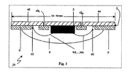
- a plated module comprising a printed circuit 2 and an integrated circuit chip 3, is represented and globally indicated with numeral reference 20.
- the printed circuit 2 comprises a plurality of conductive areas a1,.., an, generally glued through an epoxy resin 9.
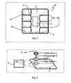
- the integrated circuit chip 3 is fixed and electrically connected through wires bonding beneath the printed circuit 2, before being sealed in a recess 6 of a generic plastic support 1, as schematically represented in figure 2 . Said electrical connections are clearly shown in figure 1 and 3 , representing respectively a top view of the printed circuit 2, sealed inside the recess 6 with the integrated circuit chip 3 beneath, and the corresponding lateral cross section.
- These contact points c1,..,ck provides communication connection between an external read write device 4 and the integrated circuit chip 3.
- the plastic support 1, in which the plated module 20 is hosted may be kept by the user in wallets or envelopes that might be protective, subject to bending or stressing forces on the plastic support 1 itself.
- the integrated circuit chip 3 is restricted to only a few millimeters in size and is protected through the printed circuit 2 from physical pressures and static electricity.
- the recess 6 is milled into the plastic support 1 using CNC machines with multiple drill bits, the dimension and location of the recess 6 being carefully controlled to meet with ISO standards.
- the solicitations act in proximity to the external circumference of the recess 6, sometimes causing the partial detaching of the integrated circuit chip 3 from the plastic support 1.
- the contact points c1..ck may be damaged, causing the communication between the integrated circuit chip 3 and the corresponding external read write device 4 to fail.
- the problem at the basis of the present invention is that of providing a plated module resistant to solicitations due to deforming, especially reducing the effect of these solicitations in proximity of the recess of a plastic support wherein the printed circuit and the integrated circuit chip resides, safeguarding the contact points that connects the conductive areas of the printed circuit to the respective bonding wires.
- a plated module including a printed circuit 2 comprising a plurality of conductive areas a 1 ,..,a n delimited by a network of insulating channels ch 1 ,..,ch n , intended for covering an integrated circuit chip 3.
- the conductive areas a 1 ,..,a n are connected through wire bonding w 1 ,..,w k to a corresponding contact point c 1 ,..,c k on the integrated circuit chip 3, so to provide communication connection between an external read write device 4 and the integrated circuit chip 3.
- the conductive areas a 1 ,..,a n bonded to contact points c 1 ,..,c k are linked to a corresponding extended or external area ea 1 ,..,ea n by one or more bridge br 1 ,.., br n .
- a plurality of additional insulating channel c k+1 delimitates an external area ea k from a nearby conductive area a 1 ,..., an or from a nearby external area ea 1 ,..., ea k .
- the insulating channels ch 1 ,..,ch k surround the conductive areas a 1 ,..,a n bonded to contact points c 1 ,..,c k as a frame, so to protect the connection with the corresponding contact point c 1 ,..,c k .
- the extended or external areas ea 1 ,..., ea k are composed of the same material used for the corresponding conductive areas a 1 ,..,a n , na 1 ,..,na n .
- the bridge br 1 ,.., br n may be constituted by the same material used for the conductive areas a 1 ,..,a n , na 1 ,..,na n , rendering easier the working process of the plated module 30 easy.
- an insulating channel b 1 divides the conductive areas a 1 ,..,a n from the nearby extended or external areas ea 1 ,..,ea m , being the insulating channel b1 crossed by a plurality of bridges br 1 ,.., br n .
- the bridges br 1 ,.., br n on the insulating channel b1 act as a mechanical bypass between an internal part (2i), including the conductive areas a 1 ,..,a n and a border parts (2a, 2b), comprising the external areas ea 1 ,..,ea m .
- the mechanical bypass is intended to render said border parts (2a, 2b) flexible respect to the internal part (2i), and to absorb solicitations on the plastic support 1, as a flexible wing in favour of the static internal part (2i).
- the internal part (2i) remains adherent to the recess 6, safeguarding the wire bonding between the conductive areas (a1, ..., an) and the contact points (cl, ..., ck) on the integrated circuit 3.
- the plated module 30 has a rounded border formed by, at least, a couple of advanced extended areas Adv 1 ,Adv n .
- the advanced extended areas Adv 1 ,..., Advn forming the round border of said plated module 30 are linked to corresponding conductive areas.
- the extended areas ea 1 ,..,ea n and the advanced extended areas form together corresponding border parts 2a, 2b at opposite sides of the core internal part 2i of the module.
- These border parts 2a, 2b may be considered wings with respect to the core internal part 2i and are linked to such an internal part 2i through the bridges br 1 ,.., br n aligned along the insulating channels b1, b2 thus forming a sort of weakening and separation lines clearly visible in figure 4 .
- the solicitations acting on the border of the recess 6 are distributed especially on external area ea 1 ,..., ea n that are passive with respect to the functioning of the integrated circuit 3.
- both the border parts 2a, 2b of the plated module 30 are rounded by corresponding couple of advanced extended areas
- the conductive areas a 1 , a n have at least a major side that is curved.
- At least one central conductive area a c has a semi-circumferential side.
- the extended areas ea 1 ,..., ea n are formed by a material different from that used for the corresponding conductive area a 1 ,..., a n .
- the external areas ea 1 ,..., ea n may be constituted by epoxy resin 9 filling the border parts 2a, 2b and absorbing solicitations acting on the border of the plated module 30.
- the epoxy resin 9, distributed on the border parts 2a, 2b, increases the adherence of the conductive areas a 1 , a n on the internal part 2i.
- the bridges br 1 , ..., br k are, according to this embodiment, in epoxy resin 9.
- the external areas ea 1 ,..., ea n are formed by a material different from the epoxy resin for example an insulating or conductive material easy coupling with the recess 6 and resistant to solicitations and pressures.
- the present invention also relates to an IC Card comprising a plated module.
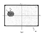
- an IC Card comprising a plated module 30 including a printed circuit 2 with a plurality of conductive areas a 1 ,..,a n , delimited by a network of insulating channels ch 1 ,..,ch n , intended for covering an integrated circuit chip 3.
- the IC card (40) also comprises a plastic support 1 with a recess 6, an integrated circuit chip 3, the plated module 30 covering the integrated circuit chip (3).
- a major surface of the plastic support 1 has a major axis x and a minor axis y of a major.
- the recess 6 on the plastic support 1 of the IC Card 40 is decentered respect the major axis x and/or the minor axis y of the plastic support 1.
- the x and y axis delimitates a quadrant q of the major surface of the plastic support 1.
- the recess 6 of the IC Card 40 is inside the quadrant q of the major surface of the plastic support 1.
- the plated module 30 according to the present invention is resistant to solicitations due to bending or deforming, especially reducing the effect of these solicitations in proximity of the recess 6 of the plastic support 1 wherein the printed circuit 2 and the integrated circuit chip 3 resides.
- the plurality of extended areas in fact, absorb solicitations near the border of recess 6 and protects the contact points cl..ck that connects the conductive areas a1,..,an of the printed circuit 1 to the respective bonding wires w1,..,wn.
- a possible break of an extended area ea 1 ,..., ea n , its detachment from the recess 6 or a dissociation with a corresponding conductive area does not cause the in utilization of the plated support 30.
Landscapes
- Engineering & Computer Science (AREA)
- Computer Hardware Design (AREA)
- Microelectronics & Electronic Packaging (AREA)
- Physics & Mathematics (AREA)
- General Physics & Mathematics (AREA)
- Theoretical Computer Science (AREA)
- Credit Cards Or The Like (AREA)
Claims (10)
- Plattiertes Modul (20) für eine IC-Karte, aufweisend
eine gedruckte Schaltung (2) und einen Chip mit integrierter Schaltung (3), wobei die gedruckte Schaltung eine Mehrzahl von leitfähigen Bereichen (a1,...,an) aufweist, die durch ein Netzwerk von isolierenden Kanälen (ch1,...,chk) begrenzt sind,
wobei das plattierte Modul dafür geeignet ist, den Chip mit der integrierten Schaltung (3), der in einer Ausnehmung (6) eines Kunststoffträgers (1) der IC-Karte untergebracht sein kann, abzudecken,
wobei einige der leitfähigen Bereiche (a1,...,an) mit entsprechenden Kontaktpunkten (c1,...,cj) des Chips mit integrierter Schaltung (3) verbunden sind
und mindestens einige der leitfähigen Bereiche (a1,...,an) über eine oder mehrere Brücken (br1,..., brl) mit einem entsprechenden erweiterten Bereich verbunden sind,
dadurch gekennzeichnet, dass
die gedruckte Schaltung ferner weitergehende erweiterte Bereiche aufweist, die mit den leitfähigen Bereichen verbunden sind, die nicht mit Kontaktpunkten der integrierten Schaltung verbunden sind,
wobei die weitergehenden erweiterten Bereiche die erweiterten Bereiche umrunden oder umgeben, die mit den leitfähigen Bereichen verbunden sind, die mit den Kontaktpunkten (c1,...,ck) der integrierten Schaltung verbunden sind,
und wobei die weitergehenden erweiterten Bereiche gerundete gegenüberliegende Seiten des plattierten Moduls bilden. - Plattiertes Modul (20) nach Anspruch 1, gekennzeichnet durch die Tatsache, dass die erweiterten Bereiche (ea1,...,eam) und/oder die Brücken (br1,...,brl) leitfähig sind.
- Plattiertes Modul (20) nach Anspruch 1, gekennzeichnet durch die Tatsache, dass die mit den Kontaktpunkten (c1,...,ck) verbundenen leitfähigen Bereiche (a1,...,an) von den erweiterten Bereichen (ea1,...,eam) und den weitergehenden erweiterten Bereichen durch isolierende Kanäle (b1, b2) getrennt sind, die von den Brücken (br1,...,brl) überquert werden.
- Plattiertes Modul (20) nach Anspruch 1 oder 2, gekennzeichnet durch die Tatsache, dass gerundete isolierende Kanäle (ch1,...,chk) die mit den Kontaktpunkten (c1,...,ck) verbundenen leitfähigen Bereiche (a1,...,an) als ein Schutzrahmen für die Kontaktpunkte (c1,...,ck) umgeben.
- Plattiertes Modul (20) nach Anspruch 4, gekennzeichnet durch die Tatsache, dass mindestens eine Hauptseite mindestens eines der leitfähigen Bereiche (a1, an) kurvenförmig ist.
- Plattiertes Modul (20) nach Anspruch 1, gekennzeichnet durch die Tatsache, dass mindestens ein in der Mitte gelegener leitfähiger Bereich (ac) der leitfähigen Bereiche (a1,...,an) eine halbkreisförmige Seite hat.
- Plattiertes Modul (20) nach Anspruch 1, gekennzeichnet durch die Tatsache, dass die erweiterten Bereiche (ea1,...,eam) und/oder die Brücken (br1,...,brl) in isolierendem Material sind.
- IC-Karte, aufweisend:- ein plattiertes Modul (20),- einen Kunsttoffträger (1) mit einer Ausnehmung (6),- einen Chip mit integrierter Schaltung (3),wobei das plattierte Modul (20) den Chip mit integrierter Schaltung (3) abdeckt, gekennzeichnet durch die Tatsache, dass das plattierte Modul gemäß einem der vorhergehenden Ansprüche 1-7 strukturiert ist.
- IC-Karte nach Anspruch 8, gekennzeichnet durch die Tatsache, dass die Ausnehmung (6) bezüglich einer Hauptachse (x) und/oder einer Nebenachse (y) einer Hauptoberfläche des Kunststoffträgers (1) dezentriert ist.
- IC-Karte nach Anspruch 9, gekennzeichnet durch die Tatsache, dass sich die Ausnehmung (6) innerhalb eines Quadranten (q) der Hauptoberfläche des Kunststoffträgers (1) befindet, der von der Haupt- und der Nebenachse (x, y) begrenzt ist.
Priority Applications (4)
| Application Number | Priority Date | Filing Date | Title |
|---|---|---|---|
| EP05028725A EP1804201B1 (de) | 2005-12-30 | 2005-12-30 | Modul einer IC-Karte |
| DE602005014498T DE602005014498D1 (de) | 2005-12-30 | 2005-12-30 | Modul einer IC-Karte |
| AT05028725T ATE431601T1 (de) | 2005-12-30 | 2005-12-30 | Modul einer ic-karte |
| US11/618,364 US7719846B2 (en) | 2005-12-30 | 2006-12-29 | Plated module for an IC card |
Applications Claiming Priority (1)
| Application Number | Priority Date | Filing Date | Title |
|---|---|---|---|
| EP05028725A EP1804201B1 (de) | 2005-12-30 | 2005-12-30 | Modul einer IC-Karte |
Publications (2)
| Publication Number | Publication Date |
|---|---|
| EP1804201A1 EP1804201A1 (de) | 2007-07-04 |
| EP1804201B1 true EP1804201B1 (de) | 2009-05-13 |
Family
ID=36423685
Family Applications (1)
| Application Number | Title | Priority Date | Filing Date |
|---|---|---|---|
| EP05028725A Expired - Lifetime EP1804201B1 (de) | 2005-12-30 | 2005-12-30 | Modul einer IC-Karte |
Country Status (4)
| Country | Link |
|---|---|
| US (1) | US7719846B2 (de) |
| EP (1) | EP1804201B1 (de) |
| AT (1) | ATE431601T1 (de) |
| DE (1) | DE602005014498D1 (de) |
Families Citing this family (130)
| Publication number | Priority date | Publication date | Assignee | Title |
|---|---|---|---|---|
| US20090159703A1 (en) | 2007-12-24 | 2009-06-25 | Dynamics Inc. | Credit, security, debit cards and the like with buttons |
| US8579203B1 (en) | 2008-12-19 | 2013-11-12 | Dynamics Inc. | Electronic magnetic recorded media emulators in magnetic card devices |
| US8931703B1 (en) | 2009-03-16 | 2015-01-13 | Dynamics Inc. | Payment cards and devices for displaying barcodes |
| US9329619B1 (en) | 2009-04-06 | 2016-05-03 | Dynamics Inc. | Cards with power management |
| US8622309B1 (en) | 2009-04-06 | 2014-01-07 | Dynamics Inc. | Payment cards and devices with budgets, parental controls, and virtual accounts |
| US10176419B1 (en) | 2009-04-06 | 2019-01-08 | Dynamics Inc. | Cards and assemblies with user interfaces |
| US8393545B1 (en) | 2009-06-23 | 2013-03-12 | Dynamics Inc. | Cards deployed with inactivated products for activation |
| US12380307B1 (en) | 2009-06-29 | 2025-08-05 | Jeffrey D. Mullen | Advanced card applications |
| US8511574B1 (en) | 2009-08-17 | 2013-08-20 | Dynamics Inc. | Advanced loyalty applications for powered cards and devices |
| US9306666B1 (en) | 2009-10-08 | 2016-04-05 | Dynamics Inc. | Programming protocols for powered cards and devices |
| US8727219B1 (en) | 2009-10-12 | 2014-05-20 | Dynamics Inc. | Magnetic stripe track signal having multiple communications channels |
| US8523059B1 (en) | 2009-10-20 | 2013-09-03 | Dynamics Inc. | Advanced payment options for powered cards and devices |
| US8393546B1 (en) | 2009-10-25 | 2013-03-12 | Dynamics Inc. | Games, prizes, and entertainment for powered cards and devices |
| US12229792B1 (en) | 2010-01-14 | 2025-02-18 | Dynamics Inc. | Systems and methods for matching online searches to in-store purchases |
| AU2011218216A1 (en) | 2010-02-16 | 2012-08-30 | Dynamics Inc. | Systems and methods for drive circuits for dynamic magnetic stripe communications devices |
| US8348172B1 (en) | 2010-03-02 | 2013-01-08 | Dynamics Inc. | Systems and methods for detection mechanisms for magnetic cards and devices |
| US10693263B1 (en) | 2010-03-16 | 2020-06-23 | Dynamics Inc. | Systems and methods for audio connectors for powered cards and devices |
| CA3121869A1 (en) | 2010-05-18 | 2011-11-24 | Dynamics Inc. | Systems and methods for cards and devices operable to communicate via light pulses and touch sensitive displays |
| USD652867S1 (en) | 2010-07-02 | 2012-01-24 | Dynamics Inc. | Multiple button interactive electronic card |
| USD672389S1 (en) | 2010-07-02 | 2012-12-11 | Dynamics Inc. | Multiple button interactive electronic card with light sources |
| USD687094S1 (en) | 2010-07-02 | 2013-07-30 | Dynamics Inc. | Multiple button interactive electronic card with light sources |
| USD652448S1 (en) | 2010-07-02 | 2012-01-17 | Dynamics Inc. | Multiple button interactive electronic card |
| USD670759S1 (en) | 2010-07-02 | 2012-11-13 | Dynamics Inc. | Multiple button interactive electronic card with light sources |
| USD652449S1 (en) | 2010-07-02 | 2012-01-17 | Dynamics Inc. | Multiple button interactive electronic card |
| USD652075S1 (en) | 2010-07-02 | 2012-01-10 | Dynamics Inc. | Multiple button interactive electronic card |
| USD674013S1 (en) | 2010-07-02 | 2013-01-08 | Dynamics Inc. | Multiple button interactive electronic card with light sources |
| USD652450S1 (en) | 2010-07-09 | 2012-01-17 | Dynamics Inc. | Multiple button interactive electronic card |
| USD651238S1 (en) | 2010-07-09 | 2011-12-27 | Dynamics Inc. | Interactive electronic card with display |
| USD651237S1 (en) | 2010-07-09 | 2011-12-27 | Dynamics Inc. | Interactive electronic card with display |
| USD665022S1 (en) | 2010-07-09 | 2012-08-07 | Dynamics Inc. | Multiple button interactive electronic card with light source |
| USD643063S1 (en) | 2010-07-09 | 2011-08-09 | Dynamics Inc. | Interactive electronic card with display |
| USD665447S1 (en) | 2010-07-09 | 2012-08-14 | Dynamics Inc. | Multiple button interactive electronic card with light source and display |
| USD651644S1 (en) | 2010-07-09 | 2012-01-03 | Dynamics Inc. | Interactive electronic card with display |
| USD653288S1 (en) | 2010-07-09 | 2012-01-31 | Dynamics Inc. | Multiple button interactive electronic card |
| USD792511S1 (en) | 2010-07-09 | 2017-07-18 | Dynamics Inc. | Display with font |
| USD652076S1 (en) | 2010-07-09 | 2012-01-10 | Dynamics Inc. | Multiple button interactive electronic card with display |
| USD792512S1 (en) | 2010-07-09 | 2017-07-18 | Dynamics Inc. | Display with font |
| USD792513S1 (en) | 2010-07-09 | 2017-07-18 | Dynamics Inc. | Display with font |
| USD666241S1 (en) | 2010-07-09 | 2012-08-28 | Dynamics Inc. | Multiple button interactive electronic card with light source |
| US8322623B1 (en) | 2010-07-26 | 2012-12-04 | Dynamics Inc. | Systems and methods for advanced card printing |
| US9818125B2 (en) | 2011-02-16 | 2017-11-14 | Dynamics Inc. | Systems and methods for information exchange mechanisms for powered cards and devices |
| US10055614B1 (en) | 2010-08-12 | 2018-08-21 | Dynamics Inc. | Systems and methods for advanced detection mechanisms for magnetic cards and devices |
| US9053398B1 (en) | 2010-08-12 | 2015-06-09 | Dynamics Inc. | Passive detection mechanisms for magnetic cards and devices |
| US10022884B1 (en) | 2010-10-15 | 2018-07-17 | Dynamics Inc. | Systems and methods for alignment techniques for magnetic cards and devices |
| US8561894B1 (en) | 2010-10-20 | 2013-10-22 | Dynamics Inc. | Powered cards and devices designed, programmed, and deployed from a kiosk |
| US9646240B1 (en) | 2010-11-05 | 2017-05-09 | Dynamics Inc. | Locking features for powered cards and devices |
| US8567679B1 (en) | 2011-01-23 | 2013-10-29 | Dynamics Inc. | Cards and devices with embedded holograms |
| US10095970B1 (en) | 2011-01-31 | 2018-10-09 | Dynamics Inc. | Cards including anti-skimming devices |
| US9836680B1 (en) | 2011-03-03 | 2017-12-05 | Dynamics Inc. | Systems and methods for advanced communication mechanisms for magnetic cards and devices |
| US8485446B1 (en) | 2011-03-28 | 2013-07-16 | Dynamics Inc. | Shielded magnetic stripe for magnetic cards and devices |
| EP3869443A1 (de) | 2011-05-10 | 2021-08-25 | Dynamics Inc. | Systeme, vorrichtungen und verfahren zur mobilbezahlungsakzeptans, mobile berechtigungen, mobile brieftaschen und kontaktlose kommunikationsmechanismen |
| USD670331S1 (en) | 2011-05-12 | 2012-11-06 | Dynamics Inc. | Interactive display card |
| USD676904S1 (en) | 2011-05-12 | 2013-02-26 | Dynamics Inc. | Interactive display card |
| USD670332S1 (en) | 2011-05-12 | 2012-11-06 | Dynamics Inc. | Interactive card |
| USD670329S1 (en) | 2011-05-12 | 2012-11-06 | Dynamics Inc. | Interactive display card |
| USD670330S1 (en) | 2011-05-12 | 2012-11-06 | Dynamics Inc. | Interactive card |
| US8628022B1 (en) | 2011-05-23 | 2014-01-14 | Dynamics Inc. | Systems and methods for sensor mechanisms for magnetic cards and devices |
| US8827153B1 (en) | 2011-07-18 | 2014-09-09 | Dynamics Inc. | Systems and methods for waveform generation for dynamic magnetic stripe communications devices |
| USD686214S1 (en) * | 2011-07-28 | 2013-07-16 | Lifenexus, Inc. | Smartcard with iChip contact pad |
| US11551046B1 (en) | 2011-10-19 | 2023-01-10 | Dynamics Inc. | Stacked dynamic magnetic stripe commmunications device for magnetic cards and devices |
| US11409971B1 (en) | 2011-10-23 | 2022-08-09 | Dynamics Inc. | Programming and test modes for powered cards and devices |
| US8950681B2 (en) | 2011-11-07 | 2015-02-10 | Blackberry Limited | Universal integrated circuit card apparatus and related methods |
| USD691610S1 (en) | 2011-11-07 | 2013-10-15 | Blackberry Limited | Device smart card |
| US8649820B2 (en) | 2011-11-07 | 2014-02-11 | Blackberry Limited | Universal integrated circuit card apparatus and related methods |
| US8960545B1 (en) | 2011-11-21 | 2015-02-24 | Dynamics Inc. | Data modification for magnetic cards and devices |
| US9619741B1 (en) | 2011-11-21 | 2017-04-11 | Dynamics Inc. | Systems and methods for synchronization mechanisms for magnetic cards and devices |
| US9064194B1 (en) | 2012-02-03 | 2015-06-23 | Dynamics Inc. | Systems and methods for spike suppression for dynamic magnetic stripe communications devices |
| US9710745B1 (en) | 2012-02-09 | 2017-07-18 | Dynamics Inc. | Systems and methods for automated assembly of dynamic magnetic stripe communications devices |
| US8888009B1 (en) | 2012-02-14 | 2014-11-18 | Dynamics Inc. | Systems and methods for extended stripe mechanisms for magnetic cards and devices |
| US9916992B2 (en) | 2012-02-20 | 2018-03-13 | Dynamics Inc. | Systems and methods for flexible components for powered cards and devices |
| US9734669B1 (en) | 2012-04-02 | 2017-08-15 | Dynamics Inc. | Cards, devices, systems, and methods for advanced payment game of skill and game of chance functionality |
| USD703208S1 (en) | 2012-04-13 | 2014-04-22 | Blackberry Limited | UICC apparatus |
| US8936199B2 (en) | 2012-04-13 | 2015-01-20 | Blackberry Limited | UICC apparatus and related methods |
| US11961147B1 (en) | 2012-04-15 | 2024-04-16 | K. Shane Cupp | Cards, devices, systems, and methods for financial management services |
| US11418483B1 (en) | 2012-04-19 | 2022-08-16 | Dynamics Inc. | Cards, devices, systems, and methods for zone-based network management |
| USD701864S1 (en) * | 2012-04-23 | 2014-04-01 | Blackberry Limited | UICC apparatus |
| US9033218B1 (en) | 2012-05-15 | 2015-05-19 | Dynamics Inc. | Cards, devices, systems, methods and dynamic security codes |
| US9064195B2 (en) | 2012-06-29 | 2015-06-23 | Dynamics Inc. | Multiple layer card circuit boards |
| USD730360S1 (en) * | 2012-06-29 | 2015-05-26 | Smart Packaging Solutions (Sps) | Contact terminal for a smart card |
| USD676487S1 (en) | 2012-08-27 | 2013-02-19 | Dynamics Inc. | Interactive electronic card with display and buttons |
| USD687887S1 (en) | 2012-08-27 | 2013-08-13 | Dynamics Inc. | Interactive electronic card with buttons |
| USD729871S1 (en) | 2012-08-27 | 2015-05-19 | Dynamics Inc. | Interactive electronic card with display and buttons |
| USD675256S1 (en) | 2012-08-27 | 2013-01-29 | Dynamics Inc. | Interactive electronic card with display and button |
| USD687489S1 (en) | 2012-08-27 | 2013-08-06 | Dynamics Inc. | Interactive electronic card with buttons |
| US12373820B1 (en) | 2012-08-27 | 2025-07-29 | Dynamics Inc. | Cards, devices, systems, and methods for a featured application management system |
| USD688744S1 (en) | 2012-08-27 | 2013-08-27 | Dynamics Inc. | Interactive electronic card with display and button |
| USD730438S1 (en) | 2012-08-27 | 2015-05-26 | Dynamics Inc. | Interactive electronic card with display and button |
| USD687488S1 (en) | 2012-08-27 | 2013-08-06 | Dynamics Inc. | Interactive electronic card with buttons |
| USD694322S1 (en) | 2012-08-27 | 2013-11-26 | Dynamics Inc. | Interactive electronic card with display buttons |
| USD730439S1 (en) | 2012-08-27 | 2015-05-26 | Dynamics Inc. | Interactive electronic card with buttons |
| USD828870S1 (en) | 2012-08-27 | 2018-09-18 | Dynamics Inc. | Display card |
| USD687490S1 (en) | 2012-08-27 | 2013-08-06 | Dynamics Inc. | Interactive electronic card with display and button |
| USD673606S1 (en) | 2012-08-27 | 2013-01-01 | Dynamics Inc. | Interactive electronic card with display and buttons |
| USD729869S1 (en) | 2012-08-27 | 2015-05-19 | Dynamics Inc. | Interactive electronic card with display and button |
| USD687095S1 (en) | 2012-08-27 | 2013-07-30 | Dynamics Inc. | Interactive electronic card with buttons |
| USD692053S1 (en) | 2012-08-27 | 2013-10-22 | Dynamics Inc. | Interactive electronic card with display and button |
| USD695636S1 (en) | 2012-08-27 | 2013-12-17 | Dynamics Inc. | Interactive electronic card with display and buttons |
| USD687487S1 (en) | 2012-08-27 | 2013-08-06 | Dynamics Inc. | Interactive electronic card with display and button |
| USD729870S1 (en) | 2012-08-27 | 2015-05-19 | Dynamics Inc. | Interactive electronic card with display and button |
| US12380474B1 (en) | 2012-08-30 | 2025-08-05 | Dynamics Inc. | Cards, devices, systems, and methods for a ratings management system |
| US11995642B1 (en) | 2012-09-05 | 2024-05-28 | Dynamics Inc. | Cards, devices, systems, and methods for a notification system |
| US11126997B1 (en) | 2012-10-02 | 2021-09-21 | Dynamics Inc. | Cards, devices, systems, and methods for a fulfillment system |
| US9010647B2 (en) | 2012-10-29 | 2015-04-21 | Dynamics Inc. | Multiple sensor detector systems and detection methods of magnetic cards and devices |
| US9659246B1 (en) | 2012-11-05 | 2017-05-23 | Dynamics Inc. | Dynamic magnetic stripe communications device with beveled magnetic material for magnetic cards and devices |
| US9010644B1 (en) | 2012-11-30 | 2015-04-21 | Dynamics Inc. | Dynamic magnetic stripe communications device with stepped magnetic material for magnetic cards and devices |
| US10949627B2 (en) | 2012-12-20 | 2021-03-16 | Dynamics Inc. | Systems and methods for non-time smearing detection mechanisms for magnetic cards and devices |
| USD750167S1 (en) | 2013-03-04 | 2016-02-23 | Dynamics Inc. | Interactive electronic card with buttons |
| USD751640S1 (en) | 2013-03-04 | 2016-03-15 | Dynamics Inc. | Interactive electronic card with display and button |
| USD765174S1 (en) | 2013-03-04 | 2016-08-30 | Dynamics Inc. | Interactive electronic card with button |
| USD751639S1 (en) | 2013-03-04 | 2016-03-15 | Dynamics Inc. | Interactive electronic card with display and button |
| USD764584S1 (en) | 2013-03-04 | 2016-08-23 | Dynamics Inc. | Interactive electronic card with buttons |
| USD750166S1 (en) | 2013-03-04 | 2016-02-23 | Dynamics Inc. | Interactive electronic card with display and buttons |
| USD777252S1 (en) | 2013-03-04 | 2017-01-24 | Dynamics Inc. | Interactive electronic card with buttons |
| USD750168S1 (en) | 2013-03-04 | 2016-02-23 | Dynamics Inc. | Interactive electronic card with display and button |
| USD765173S1 (en) | 2013-03-04 | 2016-08-30 | Dynamics Inc. | Interactive electronic card with display and button |
| US9888283B2 (en) | 2013-03-13 | 2018-02-06 | Nagrastar Llc | Systems and methods for performing transport I/O |
| USD729808S1 (en) * | 2013-03-13 | 2015-05-19 | Nagrastar Llc | Smart card interface |
| USD758372S1 (en) * | 2013-03-13 | 2016-06-07 | Nagrastar Llc | Smart card interface |
| US9647997B2 (en) | 2013-03-13 | 2017-05-09 | Nagrastar, Llc | USB interface for performing transport I/O |
| USD759022S1 (en) | 2013-03-13 | 2016-06-14 | Nagrastar Llc | Smart card interface |
| CN103530673A (zh) * | 2013-07-25 | 2014-01-22 | 上海杉德金卡信息系统科技有限公司 | 一种基于lds技术的金融pci安全设计方法 |
| US12282816B1 (en) | 2013-09-10 | 2025-04-22 | Dynamics Inc. | Cards, devices, EMV contacts, and methods of manufacturing cards, devices and EMV contacts |
| USD767024S1 (en) | 2013-09-10 | 2016-09-20 | Dynamics Inc. | Interactive electronic card with contact connector |
| USD737373S1 (en) | 2013-09-10 | 2015-08-25 | Dynamics Inc. | Interactive electronic card with contact connector |
| US10108891B1 (en) | 2014-03-21 | 2018-10-23 | Dynamics Inc. | Exchange coupled amorphous ribbons for electronic stripes |
| USD780763S1 (en) | 2015-03-20 | 2017-03-07 | Nagrastar Llc | Smart card interface |
| USD864968S1 (en) | 2015-04-30 | 2019-10-29 | Echostar Technologies L.L.C. | Smart card interface |
| US10032049B2 (en) | 2016-02-23 | 2018-07-24 | Dynamics Inc. | Magnetic cards and devices for motorized readers |
| US20210103919A1 (en) | 2019-10-06 | 2021-04-08 | Dynamics Inc. | Multi-function applet powered cards and other devices |
| USD956761S1 (en) | 2020-04-20 | 2022-07-05 | Zwipe As | Smart card |
Family Cites Families (11)
| Publication number | Priority date | Publication date | Assignee | Title |
|---|---|---|---|---|
| FR2634095A1 (fr) * | 1988-07-05 | 1990-01-12 | Bull Cp8 | Circuit imprime souple, notamment pour carte a microcircuits electroniques, et carte incorporant un tel circuit |
| DE4443767A1 (de) * | 1994-12-08 | 1996-06-13 | Giesecke & Devrient Gmbh | Elektronisches Modul und Datenträger mit elektrischem Modul |
| US5671525A (en) * | 1995-02-13 | 1997-09-30 | Gemplus Card International | Method of manufacturing a hybrid chip card |
| CA2192076C (en) * | 1995-04-13 | 2000-01-18 | Masao Gogami | Ic card and ic module |
| DE19901965A1 (de) * | 1999-01-19 | 2000-07-20 | Giesecke & Devrient Gmbh | Tragbarer Datenträger mit ausbrechbarer Minichipkarte |
| DE19906569A1 (de) * | 1999-02-17 | 2000-09-07 | Giesecke & Devrient Gmbh | Tragbarer Datenträger mit ausbrechbarer Minichipkarte |
| ATE404941T1 (de) * | 2000-02-02 | 2008-08-15 | Infineon Technologies Ag | Chipkarte mit sollbiegestellen |
| DE10101280A1 (de) * | 2001-01-12 | 2002-07-25 | Infineon Technologies Ag | Chipträger für Chipmodul |
| CN1628320B (zh) * | 2002-05-24 | 2010-04-28 | 株式会社Ntt都科摩 | 具有向后兼容的缩小尺寸的芯片卡及其适配器 |
| FR2853434B1 (fr) * | 2003-04-03 | 2005-07-01 | Oberthur Card Syst Sa | Carte a microcircuit fixee sur un support adaptateur, support de carte et procede de fabrication |
| JP2006253430A (ja) * | 2005-03-11 | 2006-09-21 | Renesas Technology Corp | 半導体装置およびその製造方法 |
-
2005
- 2005-12-30 AT AT05028725T patent/ATE431601T1/de not_active IP Right Cessation
- 2005-12-30 DE DE602005014498T patent/DE602005014498D1/de not_active Expired - Lifetime
- 2005-12-30 EP EP05028725A patent/EP1804201B1/de not_active Expired - Lifetime
-
2006
- 2006-12-29 US US11/618,364 patent/US7719846B2/en active Active
Also Published As
| Publication number | Publication date |
|---|---|
| ATE431601T1 (de) | 2009-05-15 |
| EP1804201A1 (de) | 2007-07-04 |
| US20070153487A1 (en) | 2007-07-05 |
| DE602005014498D1 (de) | 2009-06-25 |
| US7719846B2 (en) | 2010-05-18 |
Similar Documents
| Publication | Publication Date | Title |
|---|---|---|
| US7719846B2 (en) | Plated module for an IC card | |
| EP1804200B1 (de) | IC Karte mit verbesserter Leiterplatine | |
| KR101285907B1 (ko) | 전자식 인터페이스 장치 및 그 제조 방법과 시스템 | |
| EP2657889B1 (de) | Flexibles Etikett | |
| JP3980697B2 (ja) | 無線トランスポンダ | |
| CN103577872B (zh) | 具有分离的天线的芯片卡模块以及使用该模块的芯片卡嵌体 | |
| US20100109143A1 (en) | Semiconductor package and method of manufacturing the same | |
| EP1887497B1 (de) | RFID-Etikett | |
| CN106252317B (zh) | 具有集成电路模块和减小的键合接线应力的集成电路(ic)卡以及形成方法 | |
| US5965867A (en) | Data medium incorporating integrated circuits | |
| JP5351943B2 (ja) | 両面センサパッケージとして使用される装置 | |
| US6778407B2 (en) | Portable data carrier | |
| EP3836010B1 (de) | Biometrisches sensormodul zur integration in eine karte | |
| JP2019197313A (ja) | 電子部品実装基板、バンド、カード | |
| US8259455B2 (en) | Device for protecting the pins of an electronic component | |
| US20070158440A1 (en) | Semiconductor device | |
| EP0887766A2 (de) | IC-Karte mit einem Schlitz zum Schutz des IC-Moduls gegen einen äusserlichen Stress | |
| EP2791873B1 (de) | Verfahren zur herstellung von chip-karten | |
| US6495910B1 (en) | Package structure for accommodating thicker semiconductor unit | |
| JP3811677B2 (ja) | 保護封筒内にチップモジュールを有する平坦な担体の配置とその配置のための方法 | |
| CN107634055A (zh) | 静电释放保护架构 | |
| KR101369436B1 (ko) | 몰딩용 필름 및 이를 포함하는 반도체 패키지 | |
| JP4028164B2 (ja) | Icカード | |
| CN116779571B (zh) | 可翻转的半导体芯片 | |
| CN110188677B (zh) | 指纹模组及移动终端 |
Legal Events
| Date | Code | Title | Description |
|---|---|---|---|
| PUAI | Public reference made under article 153(3) epc to a published international application that has entered the european phase |
Free format text: ORIGINAL CODE: 0009012 |
|
| AK | Designated contracting states |
Kind code of ref document: A1 Designated state(s): AT BE BG CH CY CZ DE DK EE ES FI FR GB GR HU IE IS IT LI LT LU LV MC NL PL PT RO SE SI SK TR |
|
| AX | Request for extension of the european patent |
Extension state: AL BA HR MK YU |
|
| 17P | Request for examination filed |
Effective date: 20080103 |
|
| 17Q | First examination report despatched |
Effective date: 20080211 |
|
| AKX | Designation fees paid |
Designated state(s): AT BE BG CH CY CZ DE DK EE ES FI FR GB GR HU IE IS IT LI LT LU LV MC NL PL PT RO SE SI SK TR |
|
| GRAP | Despatch of communication of intention to grant a patent |
Free format text: ORIGINAL CODE: EPIDOSNIGR1 |
|
| GRAS | Grant fee paid |
Free format text: ORIGINAL CODE: EPIDOSNIGR3 |
|
| GRAA | (expected) grant |
Free format text: ORIGINAL CODE: 0009210 |
|
| AK | Designated contracting states |
Kind code of ref document: B1 Designated state(s): AT BE BG CH CY CZ DE DK EE ES FI FR GB GR HU IE IS IT LI LT LU LV MC NL PL PT RO SE SI SK TR |
|
| REG | Reference to a national code |
Ref country code: GB Ref legal event code: FG4D |
|
| REG | Reference to a national code |
Ref country code: CH Ref legal event code: EP |
|
| REG | Reference to a national code |
Ref country code: IE Ref legal event code: FG4D |
|
| REF | Corresponds to: |
Ref document number: 602005014498 Country of ref document: DE Date of ref document: 20090625 Kind code of ref document: P |
|
| PG25 | Lapsed in a contracting state [announced via postgrant information from national office to epo] |
Ref country code: ES Free format text: LAPSE BECAUSE OF FAILURE TO SUBMIT A TRANSLATION OF THE DESCRIPTION OR TO PAY THE FEE WITHIN THE PRESCRIBED TIME-LIMIT Effective date: 20090824 Ref country code: AT Free format text: LAPSE BECAUSE OF FAILURE TO SUBMIT A TRANSLATION OF THE DESCRIPTION OR TO PAY THE FEE WITHIN THE PRESCRIBED TIME-LIMIT Effective date: 20090513 Ref country code: PT Free format text: LAPSE BECAUSE OF FAILURE TO SUBMIT A TRANSLATION OF THE DESCRIPTION OR TO PAY THE FEE WITHIN THE PRESCRIBED TIME-LIMIT Effective date: 20090913 Ref country code: LT Free format text: LAPSE BECAUSE OF FAILURE TO SUBMIT A TRANSLATION OF THE DESCRIPTION OR TO PAY THE FEE WITHIN THE PRESCRIBED TIME-LIMIT Effective date: 20090513 Ref country code: FI Free format text: LAPSE BECAUSE OF FAILURE TO SUBMIT A TRANSLATION OF THE DESCRIPTION OR TO PAY THE FEE WITHIN THE PRESCRIBED TIME-LIMIT Effective date: 20090513 |
|
| NLV1 | Nl: lapsed or annulled due to failure to fulfill the requirements of art. 29p and 29m of the patents act | ||
| PG25 | Lapsed in a contracting state [announced via postgrant information from national office to epo] |
Ref country code: SE Free format text: LAPSE BECAUSE OF FAILURE TO SUBMIT A TRANSLATION OF THE DESCRIPTION OR TO PAY THE FEE WITHIN THE PRESCRIBED TIME-LIMIT Effective date: 20090813 Ref country code: IS Free format text: LAPSE BECAUSE OF FAILURE TO SUBMIT A TRANSLATION OF THE DESCRIPTION OR TO PAY THE FEE WITHIN THE PRESCRIBED TIME-LIMIT Effective date: 20090913 Ref country code: LV Free format text: LAPSE BECAUSE OF FAILURE TO SUBMIT A TRANSLATION OF THE DESCRIPTION OR TO PAY THE FEE WITHIN THE PRESCRIBED TIME-LIMIT Effective date: 20090513 Ref country code: PL Free format text: LAPSE BECAUSE OF FAILURE TO SUBMIT A TRANSLATION OF THE DESCRIPTION OR TO PAY THE FEE WITHIN THE PRESCRIBED TIME-LIMIT Effective date: 20090513 Ref country code: SI Free format text: LAPSE BECAUSE OF FAILURE TO SUBMIT A TRANSLATION OF THE DESCRIPTION OR TO PAY THE FEE WITHIN THE PRESCRIBED TIME-LIMIT Effective date: 20090513 Ref country code: NL Free format text: LAPSE BECAUSE OF FAILURE TO SUBMIT A TRANSLATION OF THE DESCRIPTION OR TO PAY THE FEE WITHIN THE PRESCRIBED TIME-LIMIT Effective date: 20090513 |
|
| PG25 | Lapsed in a contracting state [announced via postgrant information from national office to epo] |
Ref country code: EE Free format text: LAPSE BECAUSE OF FAILURE TO SUBMIT A TRANSLATION OF THE DESCRIPTION OR TO PAY THE FEE WITHIN THE PRESCRIBED TIME-LIMIT Effective date: 20090513 Ref country code: DK Free format text: LAPSE BECAUSE OF FAILURE TO SUBMIT A TRANSLATION OF THE DESCRIPTION OR TO PAY THE FEE WITHIN THE PRESCRIBED TIME-LIMIT Effective date: 20090513 Ref country code: CZ Free format text: LAPSE BECAUSE OF FAILURE TO SUBMIT A TRANSLATION OF THE DESCRIPTION OR TO PAY THE FEE WITHIN THE PRESCRIBED TIME-LIMIT Effective date: 20090513 |
|
| PG25 | Lapsed in a contracting state [announced via postgrant information from national office to epo] |
Ref country code: SK Free format text: LAPSE BECAUSE OF FAILURE TO SUBMIT A TRANSLATION OF THE DESCRIPTION OR TO PAY THE FEE WITHIN THE PRESCRIBED TIME-LIMIT Effective date: 20090513 Ref country code: BE Free format text: LAPSE BECAUSE OF FAILURE TO SUBMIT A TRANSLATION OF THE DESCRIPTION OR TO PAY THE FEE WITHIN THE PRESCRIBED TIME-LIMIT Effective date: 20090513 |
|
| PLBE | No opposition filed within time limit |
Free format text: ORIGINAL CODE: 0009261 |
|
| STAA | Information on the status of an ep patent application or granted ep patent |
Free format text: STATUS: NO OPPOSITION FILED WITHIN TIME LIMIT |
|
| PG25 | Lapsed in a contracting state [announced via postgrant information from national office to epo] |
Ref country code: BG Free format text: LAPSE BECAUSE OF FAILURE TO SUBMIT A TRANSLATION OF THE DESCRIPTION OR TO PAY THE FEE WITHIN THE PRESCRIBED TIME-LIMIT Effective date: 20090813 |
|
| 26N | No opposition filed |
Effective date: 20100216 |
|
| PG25 | Lapsed in a contracting state [announced via postgrant information from national office to epo] |
Ref country code: MC Free format text: LAPSE BECAUSE OF NON-PAYMENT OF DUE FEES Effective date: 20100701 |
|
| REG | Reference to a national code |
Ref country code: CH Ref legal event code: PL |
|
| GBPC | Gb: european patent ceased through non-payment of renewal fee |
Effective date: 20091230 |
|
| PG25 | Lapsed in a contracting state [announced via postgrant information from national office to epo] |
Ref country code: CH Free format text: LAPSE BECAUSE OF NON-PAYMENT OF DUE FEES Effective date: 20091231 Ref country code: LI Free format text: LAPSE BECAUSE OF NON-PAYMENT OF DUE FEES Effective date: 20091231 Ref country code: IE Free format text: LAPSE BECAUSE OF NON-PAYMENT OF DUE FEES Effective date: 20091230 Ref country code: GR Free format text: LAPSE BECAUSE OF FAILURE TO SUBMIT A TRANSLATION OF THE DESCRIPTION OR TO PAY THE FEE WITHIN THE PRESCRIBED TIME-LIMIT Effective date: 20090814 |
|
| PG25 | Lapsed in a contracting state [announced via postgrant information from national office to epo] |
Ref country code: GB Free format text: LAPSE BECAUSE OF NON-PAYMENT OF DUE FEES Effective date: 20091230 |
|
| PG25 | Lapsed in a contracting state [announced via postgrant information from national office to epo] |
Ref country code: RO Free format text: LAPSE BECAUSE OF FAILURE TO SUBMIT A TRANSLATION OF THE DESCRIPTION OR TO PAY THE FEE WITHIN THE PRESCRIBED TIME-LIMIT Effective date: 20090513 |
|
| PG25 | Lapsed in a contracting state [announced via postgrant information from national office to epo] |
Ref country code: LU Free format text: LAPSE BECAUSE OF NON-PAYMENT OF DUE FEES Effective date: 20091230 |
|
| PG25 | Lapsed in a contracting state [announced via postgrant information from national office to epo] |
Ref country code: HU Free format text: LAPSE BECAUSE OF FAILURE TO SUBMIT A TRANSLATION OF THE DESCRIPTION OR TO PAY THE FEE WITHIN THE PRESCRIBED TIME-LIMIT Effective date: 20091114 |
|
| PG25 | Lapsed in a contracting state [announced via postgrant information from national office to epo] |
Ref country code: TR Free format text: LAPSE BECAUSE OF FAILURE TO SUBMIT A TRANSLATION OF THE DESCRIPTION OR TO PAY THE FEE WITHIN THE PRESCRIBED TIME-LIMIT Effective date: 20090513 |
|
| PG25 | Lapsed in a contracting state [announced via postgrant information from national office to epo] |
Ref country code: CY Free format text: LAPSE BECAUSE OF FAILURE TO SUBMIT A TRANSLATION OF THE DESCRIPTION OR TO PAY THE FEE WITHIN THE PRESCRIBED TIME-LIMIT Effective date: 20090513 |
|
| REG | Reference to a national code |
Ref country code: DE Ref legal event code: R081 Ref document number: 602005014498 Country of ref document: DE Owner name: STMICROELECTRONICS INTERNATIONAL N.V., CH Free format text: FORMER OWNER: INCARD S.A., GENEVA, CH Effective date: 20130813 |
|
| REG | Reference to a national code |
Ref country code: FR Ref legal event code: TP Owner name: STMICROELECTRONICS INTERNATIONAL N.V., NL Effective date: 20140203 |
|
| REG | Reference to a national code |
Ref country code: FR Ref legal event code: PLFP Year of fee payment: 11 |
|
| REG | Reference to a national code |
Ref country code: FR Ref legal event code: PLFP Year of fee payment: 12 |
|
| REG | Reference to a national code |
Ref country code: FR Ref legal event code: PLFP Year of fee payment: 13 |
|
| PGFP | Annual fee paid to national office [announced via postgrant information from national office to epo] |
Ref country code: DE Payment date: 20191119 Year of fee payment: 15 |
|
| PGFP | Annual fee paid to national office [announced via postgrant information from national office to epo] |
Ref country code: IT Payment date: 20191121 Year of fee payment: 15 Ref country code: FR Payment date: 20191120 Year of fee payment: 15 |
|
| REG | Reference to a national code |
Ref country code: DE Ref legal event code: R119 Ref document number: 602005014498 Country of ref document: DE |
|
| PG25 | Lapsed in a contracting state [announced via postgrant information from national office to epo] |
Ref country code: IT Free format text: LAPSE BECAUSE OF NON-PAYMENT OF DUE FEES Effective date: 20201230 Ref country code: FR Free format text: LAPSE BECAUSE OF NON-PAYMENT OF DUE FEES Effective date: 20201231 |
|
| PG25 | Lapsed in a contracting state [announced via postgrant information from national office to epo] |
Ref country code: DE Free format text: LAPSE BECAUSE OF NON-PAYMENT OF DUE FEES Effective date: 20210701 |