EP1804285B1 - Verfahren zur Herstellung eines Transistors mit selbstausgerichtetem Kanal - Google Patents
Verfahren zur Herstellung eines Transistors mit selbstausgerichtetem Kanal Download PDFInfo
- Publication number
- EP1804285B1 EP1804285B1 EP05077990.9A EP05077990A EP1804285B1 EP 1804285 B1 EP1804285 B1 EP 1804285B1 EP 05077990 A EP05077990 A EP 05077990A EP 1804285 B1 EP1804285 B1 EP 1804285B1
- Authority
- EP
- European Patent Office
- Prior art keywords
- mask
- layer
- gate
- transistor
- conductive material
- Prior art date
- Legal status (The legal status is an assumption and is not a legal conclusion. Google has not performed a legal analysis and makes no representation as to the accuracy of the status listed.)
- Expired - Lifetime
Links
Images


Classifications
-
- H—ELECTRICITY
- H10—SEMICONDUCTOR DEVICES; ELECTRIC SOLID-STATE DEVICES NOT OTHERWISE PROVIDED FOR
- H10D—INORGANIC ELECTRIC SEMICONDUCTOR DEVICES
- H10D30/00—Field-effect transistors [FET]
- H10D30/60—Insulated-gate field-effect transistors [IGFET]
- H10D30/64—Double-diffused metal-oxide semiconductor [DMOS] FETs
- H10D30/66—Vertical DMOS [VDMOS] FETs
-
- H—ELECTRICITY
- H10—SEMICONDUCTOR DEVICES; ELECTRIC SOLID-STATE DEVICES NOT OTHERWISE PROVIDED FOR
- H10D—INORGANIC ELECTRIC SEMICONDUCTOR DEVICES
- H10D30/00—Field-effect transistors [FET]
- H10D30/01—Manufacture or treatment
- H10D30/021—Manufacture or treatment of FETs having insulated gates [IGFET]
- H10D30/028—Manufacture or treatment of FETs having insulated gates [IGFET] of double-diffused metal oxide semiconductor [DMOS] FETs
- H10D30/0291—Manufacture or treatment of FETs having insulated gates [IGFET] of double-diffused metal oxide semiconductor [DMOS] FETs of vertical DMOS [VDMOS] FETs
-
- H—ELECTRICITY
- H10—SEMICONDUCTOR DEVICES; ELECTRIC SOLID-STATE DEVICES NOT OTHERWISE PROVIDED FOR
- H10P—GENERIC PROCESSES OR APPARATUS FOR THE MANUFACTURE OR TREATMENT OF DEVICES COVERED BY CLASS H10
- H10P30/00—Ion implantation into wafers, substrates or parts of devices
- H10P30/20—Ion implantation into wafers, substrates or parts of devices into semiconductor materials, e.g. for doping
- H10P30/22—Ion implantation into wafers, substrates or parts of devices into semiconductor materials, e.g. for doping using masks
- H10P30/221—Ion implantation into wafers, substrates or parts of devices into semiconductor materials, e.g. for doping using masks characterised by the angle between the ion beam and the mask
-
- H—ELECTRICITY
- H10—SEMICONDUCTOR DEVICES; ELECTRIC SOLID-STATE DEVICES NOT OTHERWISE PROVIDED FOR
- H10P—GENERIC PROCESSES OR APPARATUS FOR THE MANUFACTURE OR TREATMENT OF DEVICES COVERED BY CLASS H10
- H10P30/00—Ion implantation into wafers, substrates or parts of devices
- H10P30/20—Ion implantation into wafers, substrates or parts of devices into semiconductor materials, e.g. for doping
- H10P30/222—Ion implantation into wafers, substrates or parts of devices into semiconductor materials, e.g. for doping characterised by the angle between the ion beam and the crystal planes or the main crystal surface
-
- H—ELECTRICITY
- H10—SEMICONDUCTOR DEVICES; ELECTRIC SOLID-STATE DEVICES NOT OTHERWISE PROVIDED FOR
- H10D—INORGANIC ELECTRIC SEMICONDUCTOR DEVICES
- H10D64/00—Electrodes of devices having potential barriers
- H10D64/20—Electrodes characterised by their shapes, relative sizes or dispositions
- H10D64/27—Electrodes not carrying the current to be rectified, amplified, oscillated or switched, e.g. gates
- H10D64/311—Gate electrodes for field-effect devices
- H10D64/411—Gate electrodes for field-effect devices for FETs
- H10D64/511—Gate electrodes for field-effect devices for FETs for IGFETs
- H10D64/514—Gate electrodes for field-effect devices for FETs for IGFETs characterised by the insulating layers
- H10D64/516—Gate electrodes for field-effect devices for FETs for IGFETs characterised by the insulating layers the thicknesses being non-uniform
-
- H—ELECTRICITY
- H10—SEMICONDUCTOR DEVICES; ELECTRIC SOLID-STATE DEVICES NOT OTHERWISE PROVIDED FOR
- H10D—INORGANIC ELECTRIC SEMICONDUCTOR DEVICES
- H10D64/00—Electrodes of devices having potential barriers
- H10D64/20—Electrodes characterised by their shapes, relative sizes or dispositions
- H10D64/27—Electrodes not carrying the current to be rectified, amplified, oscillated or switched, e.g. gates
- H10D64/311—Gate electrodes for field-effect devices
- H10D64/411—Gate electrodes for field-effect devices for FETs
- H10D64/511—Gate electrodes for field-effect devices for FETs for IGFETs
- H10D64/517—Gate electrodes for field-effect devices for FETs for IGFETs characterised by the conducting layers
- H10D64/519—Gate electrodes for field-effect devices for FETs for IGFETs characterised by the conducting layers characterised by their top-view geometrical layouts
Definitions
- the present invention relates to a method for manufacturing transistors comprising an electrode such as a control electrode and a doped functional element self-aligned with the electrode, such as a channel self-aligned with the control electrode as well as transistors made by the method.
- the method according to the present invention is easy to perform and the transistors obtained by this method have an improved reliability.
- Smart Power technologies have been developed in order to cope with the requirements of the ever-increasing digital content of mixed analogue/digital ASICs used in e.g. automotive, peripheral and consumer applications.
- the considered Smart Power technology allows designers to integrate complex digital and precision analog circuitry, embedded microprocessors and high-voltage functionality onto a single IC.
- the technology is suitable for a variety of applications such as sensor interfaces, transceivers and actuator and motor drivers.
- VDMOS vertical double diffused metal oxide semiconductor
- the channel of the VDMOS transistor may be formed of e.g. a p-type channel, also referred to as Pbody.
- CMOS poly patterning mask a first photoresist
- Pbody mask a second photoresist
- the double photoresist concept results in several manufacturability and reliability problems as the channel does not end up self-aligned with the edge of the gate in case the remaining photoresist after the CMOS poly patterning becomes too thin or completely removed, when a margin of approximately 0.2 to 0.4 ⁇ m has to be taken into account between the edge of the poly gate and the edge of the Pbody photoresist mask because of alignment tolerance limitation.
- the Pbody mask becomes not reworkable in case of lithography issues, meaning that if something goes wrong during the application, i.e. coating or development, of the Pbody mask, it is not possible to remove the top photoresist only and restart the operation, because the bottom photoresist remaining from the CMOS poly patterning will be removed also.
- There is a risk of partial removal or re-deposition of particles of one of the photoresist layers especially at the edge of the gate leading to local anomalies on the channel edge, e.g. local variation of the channel length.
- US 5,670,392 a method for manufacturing high-density MOS-technology power devices is described.
- the gate of the device is formed by etching windows 15 in an insulated gate layer 8 with an oxide layer 11 on top.
- the implantation mask for the source regions coincides with the implantation mask for the channel regions and for the deep body regions of the elementary functional units.
- a P type dopant such as boron, is selectively implanted into an N- layer 2 formed on an N+ substrate 1 along a direction which lies in a transversal plane, and which is tilted at an angle A3 with respect to the direction T.
- the tilt angle A3 is chosen, together with the implantation energy, to make the dopant penetrate under edge 17 of the windows 15.
- a P- type stripe 5 is thus formed around an N+ stripe 6 which extends under the insulated gate layer 8 comprising a thermally-grown thin oxide layer 9 and a polysilicon layer 10 to form a channel region of the elementary MOSFETs (see Fig. 1 ).
- the above-described steps are repeated by tilting the dopant ion beam at an angle A4 (not shown in the figure), substantially symmetrical to A3, to form in a same manner another P-type stripe 5 along the opposite edge of each window 15.
- EP 0 731 504 to manufacture an integrated circuit comprising lateral DMOS-technology power devices and non-volatile memory cells provides for: forming respective laterally displaced isolated semiconductor regions, electrically insulated from each other and from a common semiconductor substrate, inside which the devices will be formed; forming conductive insulated gate regions for the lateral DMOS-technology power devices. It also shows forming deep body regions aligned with edges of the insulated gate regions, and channel regions extending under the insulated gate regions. The channel regions are formed by means of a second implantation of a second dopant such that said channel regions are formed directly without performing a thermal diffusion at a high temperature.
- DMOS transistor structure in which a protective layer is used to protect the already essentially completed DMOS transistor structure from the negative effects of additional process steps.
- the DMOS gate electrode is structured using two lithography steps. In a first lithography step, essentially only the source region of the DMOS transistor structure is opened, whereby the electrode layer still present can be used as a mask for the subsequent production of the body region.
- field effect transistors include the steps of implanting first conductivity type dopants at a first dose level into a first portion of a relatively lightly doped drift region of first conductivity type semiconductor.
- a body region of second conductivity type semiconductor is then formed in a second portion of the semiconductor drift region.
- a gate electrode is then formed on the drift region to extend opposite the body region and the field oxide isolation region.
- Source and drain regions of first conductivity type semiconductor are then formed in the body region and in a third portion of the drift region spaced from the second portion, respectively, by implanting first conductivity type dopants at a second dose level using the gate electrode and field oxide isolation region as an implant mask.
- the invention relates to a method of manufacturing a transistor comprising control electrode and a doped channel self-aligned with the control electrode.
- An advantage of some embodiments of the present invention is based on providing a manufacturing method for transistors which is compatible with Smart Power technologies and which leads to transistors showing good reliability, preferably improved reliability with respect to prior art transistors.
- the overlap is defined by projection of the first mask onto an opening in the second mask or vice versa, according to a direction substantially perpendicular to the plane of the substrate.
- the final pattern of the control electrode is defined by the first mask with the subtraction of the overlap.
- the overlap may be up to 0.4 ⁇ m.
- implanting dopant elements in the substrate is performed under an angle, i.e. in a direction forming an angle ⁇ with a direction substantially perpendicular to the plane of the substrate, ⁇ being different from zero.
- the angle ⁇ may be between 30° and 60°, and preferably is substantially 45°.
- Implanting dopant elements in the substrate is performed using said second mask. Implanting dopant elements is performed after formation of the control electrode, hereby making use of the second mask.
- a method according to embodiments of the invention may furthermore comprise providing an insulating layer between the substrate and the layer of conductive material.
- the control electrode may be a gate.
- the transistor may be a DMOS transistor, for example a VDMOS transistor.
- the embodiments described relates to a method for manufacturing a transistor, especially one comprising a conductive electrode and a transistor internal doped functional component self-aligned with the electrode.
- An example is a transistor with a control electrode and a channel self-aligned with this control electrode.
- the method according to some embodiments of the present invention may be used to form a double diffused metal-oxide semiconductor (DMOS) transistor such as e.g. a vertical DMOS (VDMOS) transistor.
- DMOS double diffused metal-oxide semiconductor
- VDMOS vertical DMOS
- the method according to this embodiment of the present invention comprises a double etching of a layer of conductive material to form an electrode, e.g. a control electrode, e.g. gate, of a transistor.
- double etching of the layer of conductive material is meant that etching of the layer of conductive material comprises two different etching steps. Each etching step is made using a different mask.
- a first etching step is performed using a first mask and a second etching step is performed using a second mask.
- the first mask and the second mask show a common intersection feature or an overlap. This common intersection feature or overlap is not necessarily a physical common intersection feature or overlap, as both masks do not necessarily touch.
- the overlap is defined by projection of the first mask onto an opening of the second mask according to a direction substantially perpendicular to the plane of the substrate.
- a final pattern of the conductive electrode, e.g. of the control electrode, is then defined by the second mask with a subtraction of the overlap.
- the method furthermore comprises implanting dopant elements to form a channel in a substrate.
- the method according to the present invention leads to a transistor comprising a control electrode and a self-aligned channel.
- implantation of dopant elements in order to form a channel may be performed by means of a tilted implantation.
- tilted implantation is meant an implantation in a direction forming an angle ⁇ with a direction substantially perpendicular to the plane of the substrate, ⁇ being different from zero.
- the angle ⁇ may be between 30° and 60° and may preferably be substantially 45°.
- substantially 45° is meant an angle of 45° including a deviation of at most 5%. For a tilt of 30°, a shorter channel is obtained and a deeper Pbody. The shorter the channel, the more it may become critical in terms of leakage current and lateral punch-through.
- the method according to embodiments of the present invention comprises in a first step providing a substrate.
- the term "substrate” may include any underlying material or materials that may be used, or upon which a device, a circuit or an epitaxial layer may be formed.
- this "substrate” may include a semiconductor substrate such as e.g. a doped silicon, a gallium arsenide (GaAs), a gallium arsenide phosphide (GaAsP), an indium phosphide (InP), a germanium (Ge), or a silicon germanium (SiGe) substrate.
- the "substrate” may include for example, an insulating layer such as a SiO 2 or a Si 3 N 4 layer in addition to a semiconductor substrate portion.
- the term substrate also includes silicon-on-glass, silicon-on sapphire substrates.
- substrate is thus used to define generally the elements for layers that underlie a layer or portions of interest.
- the "substrate” may be any other base on which a layer is formed, for example a glass or metal layer.
- the insulating layer may be formed of any suitable insulating layer, such as e.g. an oxide layer (e.g. SiO2), a nitride layer (e.g. Si 3 N 4 ).
- the insulating layer may be an oxide layer, most preferably the insulating layer may be a silicon oxide (SiO 2 ) layer.
- a layer of conductive material is provided.
- the layer of conductive material may be formed of any suitable conductive material.
- the layer of conductive material may be formed of a semiconductor material (e.g. polysilicon), a metal (e.g. gold or aluminium), or may be formed of another material such as an inorganic material e.g. indium tin oxide (ITO).
- the layer of conductive material may be a polysilicon layer.
- the layer of conductive material is etched in two steps, each step using a different mask.
- a first etching step is performed using a first mask and a second etching step is performed using a second mask.
- the first and second masks show a common intersection feature or overlap.
- a final pattern of the conductive material, e.g. control electrode is defined by the first mask with a subtraction of the overlap.
- the etching of the layer of conductive material in two steps may also be referred to as double etching of the layer of conductive material.
- implantation of dopant elements may be performed by a tilted implant of dopant elements in the substrate using the second mask.
- tilted implant is meant an implant of dopant elements in a direction making a non-zero angle with a direction substantially perpendicular to the plane of the substrate, as described above, preferably an angle between 30 and 60°, more preferred an angle of substantially 45°.
- substantially 45° is meant an angle of 45° including a deviation of at most 5%.
- VDMOS vertical double diffused metal oxide semiconductor
- a substrate 20 is provided in a first step.
- the term "substrate” may include any suitable material or layer as described above.
- an insulating layer may be provided on top of the substrate 20.
- the insulating layer may be a gate insulating layer, preferably a gate oxide layer, which may for example be formed of SiO 2 .
- the insulating layer will therefore be referred to as gate insulating layer and can be an oxide layer. Again, this is only for the ease of explanation and is not limiting the invention in any way.
- a layer 21 of a conductive material is deposited. This may be done by means of any suitable technique known by a person skilled in the art, such as, for example, chemical vapour deposition (CVD) or related techniques such as plasma enhanced CVD (PECVD).
- CVD chemical vapour deposition
- PECVD plasma enhanced CVD
- the layer 21 of conductive material may be formed of polysilicon.
- any other suitable conductive material such as e.g. a metal, an inorganic conductive material or another semiconductor material, may be used to form the layer 21 of conductive material.
- the layer 21 of conductive material will further be referred to as a layer 21 of gate material.
- a first layer of photoresist material may be deposited on top of the layer 21 of conductive material, in this embodiment on top of the gate material. This may be done by any suitable means, for example, by spincoating or printing.
- the first layer of photoresist may be made of any suitable polymer that can be used as a photoresist, such as for example poly(vinyl cinnamate) or novolak-based polymers.
- the first layer of photoresist material may have a thickness of a few ⁇ m. For patterning the first layer of photoresist, this layer may be illuminated through a suitable mask e.g. by means of UV light.
- the first layer of photoresist material may be developed by which either the illuminated parts of the photoresist (positive resist) or the non-illuminated parts of the photoresist (negative resist) are removed, depending on which type of photoresist has been used.
- the first layer of photoresist material may be patterned to form a first mask 22, in this preferred embodiment a gate mask 22.
- the first layer of resist material may be patterned by means of an electron beam.
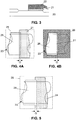
- Fig. 2A and 2B respectively illustrate a top view and a cross-section of the structure obtained after the formation of the first mask 22, in this first embodiment the gate mask.
- reference number 23 indicates the active region of the device to be formed.
- a next step exposed parts of the layer 21 of conductive material, in the example given the gate material, or in other words those parts of layer 21 which are not covered by the first mask 22, in this embodiment the gate mask, are removed. This may, for example, be done by dry or wet etching.
- This step represents a first etching step performed on the layer 21 of conductive material, in this first embodiment the gate material, using the first mask 22, in the example given the gate mask. The result of this first etching step is illustrated in Fig. 3 .
- the gate mask 22 may then be removed e.g. by using an organic solvent.
- a second layer of photoresist material may be applied to the structure so far obtained e.g. by means of spincoating or printing.
- the second layer of photoresist material may be made of any suitable polymer that can be used as a photoresist, such as for example poly(vinyl cinnamate) or novolak-based polymers.
- the second layer of photoresist material may then be patterned so as to form a second mask 25, in this first embodiment a body mask 25, and to define a body window 26. Patterning of the second layer of photoresist material may be performed in a similar way as described hereinabove for the first layer of photoresist material.
- the structure obtained so far is illustrated in Fig.
- FIG. 4A and 4B which both show the result after patterning the second layer of photoresist material, and thus after formation of the second mask 25, in this first embodiment the body mask 25.
- Fig. 4A only shows the second mask 25 in dashed lines.
- Fig. 4B the complete second mask 25 is illustrated.
- the second mask 25, in this first embodiment the body mask shows an overlap O with the patterned layer 21 of conductive material, in the example given gate material.
- the overlap O is defined by projection of the first mask 22 onto an opening of the second mask 25 or vice versa, according to a direction substantially perpendicular to the plane of the substrate. The overlap is advantageous for absorbing alignment tolerances in photolithographic processes.
- the first mask is aligned to a certain reference, in general the active area, with a certain tolerance in the range of 0.1 ⁇ m to 0.2 ⁇ m for sub-half micrometer Smart Power technologies.
- the second mask may be aligned to the same reference as the first mask, as well as to the resulting patterns from the first mask itself, with again some tolerance in the same order of magnitude in general. If the second mask is not aligned to the first mask, then the cumulative alignment tolerance has to be taken into account, meaning the range may extend to 0.4 ⁇ m if the above-mentioned values are considered.
- the gate mask Because of the overlap O between the opening in the second mask 25, in this embodiment the body mask and the first mask 22, in this embodiment the gate mask, at this stage of the process, there is some conductive material, in this first embodiment gate material, remaining in the opening of the body window 26, as is illustrated in Fig. 4A and 4B .
- a second etch of the conductive material, in this embodiment gate material is performed to remove this exposed intersection feature.
- the above-described steps result in a self-aligned gate edge and body mask edge.
- the second mask 25, in this first embodiment body mask is only shown in dashed lines.
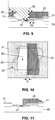
- an implantation of dopant elements may be performed to form a body layer 27 in the substrate 20.
- the range of dopant elements used may vary depending on the type of transistor made, e.g. lateral or vertical DMOS, and also on the shape of the elementary cell, e.g. longitudinal stripes or polygonal or circular.
- a quad implant with a dose of four times 5E12 to 1E13 cm -2 may be performed to cover the four possible orientations of the transistor on the wafer, each implant being twisted by 90° by reference to the former implant.
- the energy used for the implantation may be in the range of e.g. 120 keV to 180 keV for boron.
- the implant might need to be circular or multi-angular.
- the implantation of dopant elements is performed using the second mask 25, in this embodiment the body mask.
- the implantation may be performed in a direction, indicated by arrows 28 in Fig. 6 , forming an angle ⁇ different from zero with a direction substantially perpendicular to the plane of the substrate 20 as illustrated in Fig. 6 .
- the angle ⁇ may be between 30° and 60°.
- the angle ⁇ may be substantially 45°, as disclosed above.
- a body layer 27 and a channel 29 are formed. The channel is self-aligned to an edge of the control electrode 24, in this first embodiment the gate of the VDMOS transistor, as is illustrated in Fig. 6 .
- the second mask 25, in this first embodiment the body mask may be removed by e.g. stripping.
- the final result of the transistor, in this preferred embodiment, a VDMOS transistor, after the process according to the first embodiment of the present invention is illustrated in Fig. 7 .
- the transistor, in the example given the VDMOS transistor, according to the first embodiment of the present invention may further be finished in a conventional way known by a person skilled in the art.
- contact regions, first and second main electrodes, e.g. source and drain regions and source and drain electrodes may be formed in any suitable way known by a person skilled in the art.
- the final pattern of the control electrode 24, in the example given the gate is defined by the first mask 22, in this embodiment the gate mask, however subtracting the common intersection feature or overlap O between the first mask 22 and the opening in the second mask 25.
- the final pattern of the control electrode 24, e.g. gate results from the double etching of the control electrode, e.g. gate 24, which is a basic idea of embodiments of the present invention.
- the method according to the first embodiment of the present invention leads to a transistor, e.g. a VDMOS transistor, with a control electrode 24, in the example given a gate, and a with the control electrode 24 self-aligned channel 29.
- the method according to this second method may in a first step comprise providing a substrate 20.
- substrate may include any suitable material or layer as described above.
- the insulating layer may be a gate insulating layer, e.g. a gate oxide layer, which may preferably be formed of SiO 2 .
- the insulating layer will be referred to as gate insulating layer. Again, this is only for the ease of explanation and is not limiting the invention in any way.
- a layer 21 of a conductive material is deposited. This may be done by means of any suitable technique known by a person skilled in the art, such as chemical vapour deposition (CVD) or related techniques such as plasma enhanced CVD (PECVD).
- the layer 21 of conductive material may be formed of polysilicon.
- any other suitable conductive material such as e.g. a metal, an inorganic conductive material or another semiconductor material, may be used to form the layer 21 of conductive material.
- a VDMOS transistor is described comprising a gate.
- the layer 21 of conductive material will further be referred to as a layer 21 of gate material.
- a first layer of photoresist material may be provided on top of the layer 21 of conductive material, in the method given the gate material. This may be done by any suitable technique known by a person skilled in the art, for example by means of spincoating or printing.
- the first layer of photoresist material may be made of any suitable polymer that can be used as a photoresist, such as for example poly(vinyl cinnamate) or novolak-based polymers.
- the first layer of photoresist material may have a thickness of a few ⁇ m.
- the first layer of photoresist material may be illuminated through a suitable mask e.g. by means of UV light in order to pattern it.
- the photoresist may be developed by which either the illuminated parts of the photoresist (positive resist) or the non-illuminated parts of the photoresist (negative resist) are removed, depending on which type of photoresist has been used.
- the first layer of photoresist material may be patterned to form a first mask 22, in this second method a body mask.
- the first mask 22, in this second method the body mask defines an opening or body window 26 through which part of the layer 21 of conductive material, in this second method the gate material, is exposed, as illustrated in Fig. 8 .
- the layer 21 of conductive material, in this method the gate material may be etched through the opening or body window 26 in the first mask 22, in this second method the body mask.
- Fig. 8 illustrates a top view of the device after performing the above described steps, i.e. after patterning of the first mask 22, in this second method the body mask, and after etching of the layer 21 of conductive material, in this second method the gate material. These steps result in self-aligned gate edge and body mask edge.
- implantation of dopant elements may be performed using the first mask 22, in this second method the body mask, and the conductive material underneath.
- the implantation may be performed in a direction, indicated by arrows 28 in Fig. 9 , forming an angle ⁇ different from zero with a direction substantially perpendicular to the plane of the substrate 20 as illustrated in Fig. 9 .
- the angle ⁇ may be between 30° and 60°.
- the angle ⁇ may be substantially 45°.
- the body mask may be removed by e.g. stripping, and a second layer of photoresist material may be deposited and patterned.
- the second layer of photoresist material may for example have a thickness of a few ⁇ m.
- the second layer of photoresist material may be patterned in a similar way as already described above in order to form a second mask 25, in this second method a gate mask.
- the second layer of photoresist material may be patterned such that the second mask 25, in this method the gate mask, shows an overlap O with the opening in the first mask 22, in this method the body mask (see Fig. 10 ).
- the overlap O may be such that a sufficient overlap margin is obtained between the resulting second mask 25, in this second method the gate mask, and the control electrode 24, in this second method the gate, in order to protect the edge of the gate 24 of the VDMOS transistor from any influence of next process steps, such as for example an etch step.
- sufficient overlap margin is meant that the overlap must be big enough to cope with the alignment tolerance limits as explained above.
- the overlap is meant to avoid re-etching of the edge of the gate during the second gate etching and after the Pbody implant in order to keep a perfectly self-aligned channel with a constant length.
- the size of the overlap depends on the alignment tolerance as explained above. The above is illustrated in Fig. 10 and 11 which respectively show a top view and a cross-section of the device formed up till now.
- the layer 21 of conductive material in this second method the gate material, may be etched a second time, now using the second mask 25, in this method the gate mask.
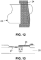
- the second mask 25 may be removed by, for example, stripping. This results in the final pattern of the control electrode 24, in this second method the gate, of the VDMOS transistor. This is illustrated in Fig. 12 and 13 which respectively show a top view and a cross-section of the transistor, in the example given the VDMOS transistor.
- the electronic device i.e. the VDMOS transistor, according to the preferred embodiment of the present invention may further be finished in a conventional way known by a person skilled in the art.
- contact regions, first and second main electrodes, e.g. source and drain regions and source and drain electrodes, may be formed in any suitable way known by a person skilled in the art.
- the final pattern of the control electrode 24, in this embodiment the gate, of the transistor may be defined by the pattern of the second mask 25, however subtracting the intersection feature or overlap.
- the final pattern of the control electrode 24, e.g. gate results from the double etching of the control electrode 24, e.g. gate, which is the basic idea of embodiments of the present invention.
- the method according to the second method leads to a transistor, e.g. a VDMOS transistor, with a control electrode 24, in the example given a gate, and a self-aligned channel 29.
- the method according to embodiments of the present invention is useful for any technology with an electrode such as a control electrode and a functional element self-aligned with the electrode, such as a channel self-aligned with the control electrode, and is particularly useful for use in Smart Power technologies. Therefore, the present invention includes a method according to any of the embodiments as described above, used in Smart Power technologies.
Landscapes
- Insulated Gate Type Field-Effect Transistor (AREA)
- Electrodes Of Semiconductors (AREA)
Claims (9)
- Verfahren zum Herstellen eines Transistors, der eine Steuerungselektrode (24) und einen Kanal (29), der sich selbst auf die Steuerungselektrode ausgerichtet hat, umfasst, wobei das Verfahren umfasst, dass:- ein Substrat (20) bereitgestellt wird,- eine Schicht (21) aus leitfähigem Material auf dem Substrat (20) bereitgestellt wird,- aus der Schicht (21) aus leitfähigem Material eine Steuerungselektrode (24) mit einem endgültigen Muster ausgebildet wird, indem:- eine erste Maske (22) bereitgestellt wird,- die Schicht (21) aus leitfähigem Material unter Verwendung der ersten Maske (22) geätzt wird, und anschließend- eine zweite Maske (25) bereitgestellt wird,
wobei die geätzte Schicht (21) aus leitfähigem Material und eine Öffnung in der zweiten Maske (25) eine Überschneidung (O) aufweisen,- die Schicht (21) aus leitfähigem Material unter Verwendung der zweiten Maske (25) geätzt wird, und anschließend- Dotierungselemente in das Substrat (20) implantiert werden, um den Kanal (29) unter Verwendung der zweiten Maske (25) auszubilden,wobei
das endgültige Muster der Steuerungselektrode (24) durch die erste Maske (22) samt Subtraktion der Überschneidung (O) definiert wird. - Verfahren nach Anspruch 1, wobei die Überschneidung (O) zwischen der ersten Maske (22) und der Öffnung in der zweiten Maske (25) eine Überschneidungstiefe von bis zu 0,4 µm aufweist.
- Verfahren nach Anspruch 1 oder 2, wobei das Substrat (20) in einer Ebene liegt, wobei das Implantieren von Dotierungselementen in das Substrat (20) in eine Richtung ausgeführt wird, die mit einer Richtung im Wesentlichen rechtwinklig zu der Ebene des Substrats (20) einen Winkel α bildet, wobei α von null verschieden ist.
- Verfahren nach Anspruch 3, wobei der Winkel α zwischen 30° und 60° liegt.
- Verfahren nach Anspruch 4, wobei der Winkel α 45° beträgt.
- Verfahren nach einem der vorstehenden Ansprüche, das darüber hinaus umfasst, dass eine Isolationsschicht zwischen dem Substrat (20) und der Schicht (21) aus leitfähigem Material bereitgestellt wird.
- Verfahren nach einem der vorstehenden Ansprüche, wobei die Steuerungselektrode (24) ein Gate ist.
- Verfahren nach einem der vorstehenden Ansprüche, wobei der Transistor ein DMOS-Transistor ist.
- Verfahren nach Anspruch 8, wobei der DMOS-Transistor ein VDMOS-Transistor ist.
Priority Applications (1)
| Application Number | Priority Date | Filing Date | Title |
|---|---|---|---|
| EP05077990.9A EP1804285B1 (de) | 2005-12-27 | 2005-12-27 | Verfahren zur Herstellung eines Transistors mit selbstausgerichtetem Kanal |
Applications Claiming Priority (1)
| Application Number | Priority Date | Filing Date | Title |
|---|---|---|---|
| EP05077990.9A EP1804285B1 (de) | 2005-12-27 | 2005-12-27 | Verfahren zur Herstellung eines Transistors mit selbstausgerichtetem Kanal |
Publications (2)
| Publication Number | Publication Date |
|---|---|
| EP1804285A1 EP1804285A1 (de) | 2007-07-04 |
| EP1804285B1 true EP1804285B1 (de) | 2018-10-24 |
Family
ID=35886381
Family Applications (1)
| Application Number | Title | Priority Date | Filing Date |
|---|---|---|---|
| EP05077990.9A Expired - Lifetime EP1804285B1 (de) | 2005-12-27 | 2005-12-27 | Verfahren zur Herstellung eines Transistors mit selbstausgerichtetem Kanal |
Country Status (1)
| Country | Link |
|---|---|
| EP (1) | EP1804285B1 (de) |
Family Cites Families (5)
| Publication number | Priority date | Publication date | Assignee | Title |
|---|---|---|---|---|
| US4232439A (en) * | 1976-11-30 | 1980-11-11 | Vlsi Technology Research Association | Masking technique usable in manufacturing semiconductor devices |
| EP0731504B1 (de) * | 1995-03-09 | 2002-11-27 | STMicroelectronics S.r.l. | Verfahren zur Herstellung von intergrierten Schaltungen mit Hochspannungs- und Niederspannungs-lateralen-DMOS-Leistungsbauelementen und nichtflüchtigen Speicherzellen |
| KR100225411B1 (ko) * | 1997-03-24 | 1999-10-15 | 김덕중 | LDMOS(a lateral double-diffused MOS) 트랜지스터 소자 및 그의 제조 방법 |
| DE10053428A1 (de) * | 2000-10-27 | 2002-05-16 | Infineon Technologies Ag | Verfahren zur Herstellung eines DMOS-Transistors |
| SE519382C2 (sv) * | 2000-11-03 | 2003-02-25 | Ericsson Telefon Ab L M | Integrering av självinriktade MOS-högspänningskomponenter samt halvledarstruktur innefattande sådana |
-
2005
- 2005-12-27 EP EP05077990.9A patent/EP1804285B1/de not_active Expired - Lifetime
Non-Patent Citations (1)
| Title |
|---|
| None * |
Also Published As
| Publication number | Publication date |
|---|---|
| EP1804285A1 (de) | 2007-07-04 |
Similar Documents
| Publication | Publication Date | Title |
|---|---|---|
| US5413949A (en) | Method of making self-aligned MOSFET | |
| US5960291A (en) | Asymmetric channel transistor and method for making same | |
| JPH0130312B2 (de) | ||
| KR970023995A (ko) | 트렌치 소자분리 방법 | |
| EP0683531B1 (de) | MOSFET mit LDD Struktur und Verfahren zur Herstellung | |
| US4675981A (en) | Method of making implanted device regions in a semiconductor using a master mask member | |
| US11876018B2 (en) | Self-aligned trench MOSFET contacts having widths less than minimum lithography limits | |
| KR100351894B1 (ko) | 싱글 일렉트론 트랜지스터 제조방법 | |
| EP1804285B1 (de) | Verfahren zur Herstellung eines Transistors mit selbstausgerichtetem Kanal | |
| CN100459052C (zh) | 形成具有特定尺寸的栅极侧壁间隔件之半导体装置的方法 | |
| US6155537A (en) | Deep submicron MOS transistors with a self-aligned gate electrode | |
| US7682955B1 (en) | Method for forming deep well of power device | |
| KR20050069111A (ko) | 자기 정렬 바이폴라 트랜지스터 형성 방법 | |
| KR100258881B1 (ko) | 반도체 소자의 제조 방법 | |
| KR20040019167A (ko) | 고전압 트랜지스터의 제조방법 | |
| US12243778B2 (en) | Self-aligned semiconductor device contacts having widths less than minimum lithography limits | |
| CN113540234B (zh) | 自对准的沟槽式场效应晶体管及其制备方法 | |
| KR100790742B1 (ko) | 트랜지스터 및 그 제조방법 | |
| KR100414231B1 (ko) | 반도체소자의 제조방법 | |
| CN100461372C (zh) | 高压金属氧化物半导体元件 | |
| KR100414375B1 (ko) | 마스크롬 제조 방법 | |
| KR100266689B1 (ko) | 고전압 수평 확산 모스 트랜지스터 제조방법 | |
| KR100395911B1 (ko) | 반도체 소자의 제조 방법 | |
| CN116632062A (zh) | 中压晶体管及其制作方法 | |
| KR100231603B1 (ko) | 반도체소자의 트랜지스터 제조방법 |
Legal Events
| Date | Code | Title | Description |
|---|---|---|---|
| PUAI | Public reference made under article 153(3) epc to a published international application that has entered the european phase |
Free format text: ORIGINAL CODE: 0009012 |
|
| AK | Designated contracting states |
Kind code of ref document: A1 Designated state(s): AT BE BG CH CY CZ DE DK EE ES FI FR GB GR HU IE IS IT LI LT LU LV MC NL PL PT RO SE SI SK TR |
|
| AX | Request for extension of the european patent |
Extension state: AL BA HR MK YU |
|
| 17P | Request for examination filed |
Effective date: 20070725 |
|
| AKX | Designation fees paid |
Designated state(s): DE FR GB IT |
|
| 17Q | First examination report despatched |
Effective date: 20080729 |
|
| RAP1 | Party data changed (applicant data changed or rights of an application transferred) |
Owner name: SEMICONDUCTOR COMPONENTS INDUSTRIES, LLC |
|
| GRAP | Despatch of communication of intention to grant a patent |
Free format text: ORIGINAL CODE: EPIDOSNIGR1 |
|
| RIC1 | Information provided on ipc code assigned before grant |
Ipc: H01L 21/336 20060101AFI20180424BHEP Ipc: H01L 21/265 20060101ALI20180424BHEP Ipc: H01L 29/78 20060101ALI20180424BHEP Ipc: H01L 29/423 20060101ALN20180424BHEP |
|
| INTG | Intention to grant announced |
Effective date: 20180515 |
|
| GRAS | Grant fee paid |
Free format text: ORIGINAL CODE: EPIDOSNIGR3 |
|
| GRAA | (expected) grant |
Free format text: ORIGINAL CODE: 0009210 |
|
| AK | Designated contracting states |
Kind code of ref document: B1 Designated state(s): DE FR GB IT |
|
| REG | Reference to a national code |
Ref country code: GB Ref legal event code: FG4D |
|
| REG | Reference to a national code |
Ref country code: DE Ref legal event code: R096 Ref document number: 602005054828 Country of ref document: DE |
|
| REG | Reference to a national code |
Ref country code: DE Ref legal event code: R097 Ref document number: 602005054828 Country of ref document: DE |
|
| PLBE | No opposition filed within time limit |
Free format text: ORIGINAL CODE: 0009261 |
|
| STAA | Information on the status of an ep patent application or granted ep patent |
Free format text: STATUS: NO OPPOSITION FILED WITHIN TIME LIMIT |
|
| 26N | No opposition filed |
Effective date: 20190725 |
|
| PGFP | Annual fee paid to national office [announced via postgrant information from national office to epo] |
Ref country code: DE Payment date: 20191119 Year of fee payment: 15 |
|
| PGFP | Annual fee paid to national office [announced via postgrant information from national office to epo] |
Ref country code: FR Payment date: 20191120 Year of fee payment: 15 Ref country code: IT Payment date: 20191121 Year of fee payment: 15 |
|
| PGFP | Annual fee paid to national office [announced via postgrant information from national office to epo] |
Ref country code: GB Payment date: 20191122 Year of fee payment: 15 |
|
| REG | Reference to a national code |
Ref country code: DE Ref legal event code: R119 Ref document number: 602005054828 Country of ref document: DE |
|
| GBPC | Gb: european patent ceased through non-payment of renewal fee |
Effective date: 20201227 |
|
| PG25 | Lapsed in a contracting state [announced via postgrant information from national office to epo] |
Ref country code: IT Free format text: LAPSE BECAUSE OF NON-PAYMENT OF DUE FEES Effective date: 20201227 Ref country code: FR Free format text: LAPSE BECAUSE OF NON-PAYMENT OF DUE FEES Effective date: 20201231 |
|
| PG25 | Lapsed in a contracting state [announced via postgrant information from national office to epo] |
Ref country code: DE Free format text: LAPSE BECAUSE OF NON-PAYMENT OF DUE FEES Effective date: 20210701 Ref country code: GB Free format text: LAPSE BECAUSE OF NON-PAYMENT OF DUE FEES Effective date: 20201227 |