EP1804304A2 - Appareil à luminescence et procédé de sa fabrication - Google Patents
Appareil à luminescence et procédé de sa fabrication Download PDFInfo
- Publication number
- EP1804304A2 EP1804304A2 EP06027021A EP06027021A EP1804304A2 EP 1804304 A2 EP1804304 A2 EP 1804304A2 EP 06027021 A EP06027021 A EP 06027021A EP 06027021 A EP06027021 A EP 06027021A EP 1804304 A2 EP1804304 A2 EP 1804304A2
- Authority
- EP
- European Patent Office
- Prior art keywords
- light emitting
- emitting device
- phosphor
- substrate
- light
- Prior art date
- Legal status (The legal status is an assumption and is not a legal conclusion. Google has not performed a legal analysis and makes no representation as to the accuracy of the status listed.)
- Granted
Links
Images





Classifications
-
- H—ELECTRICITY
- H10—SEMICONDUCTOR DEVICES; ELECTRIC SOLID-STATE DEVICES NOT OTHERWISE PROVIDED FOR
- H10H—INORGANIC LIGHT-EMITTING SEMICONDUCTOR DEVICES HAVING POTENTIAL BARRIERS
- H10H20/00—Individual inorganic light-emitting semiconductor devices having potential barriers, e.g. light-emitting diodes [LED]
- H10H20/80—Constructional details
- H10H20/85—Packages
- H10H20/851—Wavelength conversion means
- H10H20/8515—Wavelength conversion means not being in contact with the bodies
-
- H—ELECTRICITY
- H10—SEMICONDUCTOR DEVICES; ELECTRIC SOLID-STATE DEVICES NOT OTHERWISE PROVIDED FOR
- H10H—INORGANIC LIGHT-EMITTING SEMICONDUCTOR DEVICES HAVING POTENTIAL BARRIERS
- H10H20/00—Individual inorganic light-emitting semiconductor devices having potential barriers, e.g. light-emitting diodes [LED]
- H10H20/80—Constructional details
- H10H20/85—Packages
- H10H20/851—Wavelength conversion means
- H10H20/8511—Wavelength conversion means characterised by their material, e.g. binder
-
- H—ELECTRICITY
- H10—SEMICONDUCTOR DEVICES; ELECTRIC SOLID-STATE DEVICES NOT OTHERWISE PROVIDED FOR
- H10H—INORGANIC LIGHT-EMITTING SEMICONDUCTOR DEVICES HAVING POTENTIAL BARRIERS
- H10H20/00—Individual inorganic light-emitting semiconductor devices having potential barriers, e.g. light-emitting diodes [LED]
- H10H20/01—Manufacture or treatment
- H10H20/036—Manufacture or treatment of packages
- H10H20/0361—Manufacture or treatment of packages of wavelength conversion means
-
- H—ELECTRICITY
- H10—SEMICONDUCTOR DEVICES; ELECTRIC SOLID-STATE DEVICES NOT OTHERWISE PROVIDED FOR
- H10H—INORGANIC LIGHT-EMITTING SEMICONDUCTOR DEVICES HAVING POTENTIAL BARRIERS
- H10H20/00—Individual inorganic light-emitting semiconductor devices having potential barriers, e.g. light-emitting diodes [LED]
- H10H20/80—Constructional details
- H10H20/85—Packages
- H10H20/8506—Containers
-
- H—ELECTRICITY
- H10—SEMICONDUCTOR DEVICES; ELECTRIC SOLID-STATE DEVICES NOT OTHERWISE PROVIDED FOR
- H10W—GENERIC PACKAGES, INTERCONNECTIONS, CONNECTORS OR OTHER CONSTRUCTIONAL DETAILS OF DEVICES COVERED BY CLASS H10
- H10W90/00—Package configurations
- H10W90/701—Package configurations characterised by the relative positions of pads or connectors relative to package parts
- H10W90/721—Package configurations characterised by the relative positions of pads or connectors relative to package parts of bump connectors
- H10W90/724—Package configurations characterised by the relative positions of pads or connectors relative to package parts of bump connectors between a chip and a stacked insulating package substrate, interposer or RDL
Definitions
- the present invention relates to a light emitting apparatus and a manufacturing method therefor, and relates particularly to a light emitting apparatus wherein a light emitting device is closely covered by a light transmitting substrate and a light emitting device accommodating body, or a light transmitting member and a substrate, and a manufacturing method therefor.
- a light emitting apparatus is constituted by a light emitting device, a substrate to which the light emitting device is electrically connected and phosphor, and for this light emitting apparatus chromaticity is important.
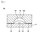
- chromaticity there is one example conventional light emitting apparatus wherein a light transmitting member is so located that the upper face and the side faces of a light emitting device are enclosed, and phosphor is so positioned that the face of the light emitting member, opposite to the light emitting device, is covered (see Fig. 1).
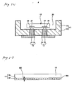
- Fig. 1 is a cross-sectional view of a conventional light emitting apparatus.
- a light emitting apparatus 100 includes a light emitting device 102, a light transmitting member 103 and a phosphor 105.
- the substrate 101 is plate shaped and includes a wiring pattern (not shown).
- the light emitting device 102 is electrically connected to the wiring pattern (not shown) formed on the substrate 101.
- the light transmitting member 103 includes a recessed portion 104 that encloses the side faces and the upper face of the light emitting device 102, and includes a function that permits the passage of light emitted by the light emitting device 102.
- the phosphor 105 is located so as to cover a face 103A of the light transmitting member 103 opposite to the recessed portion 104. These two components are bonded together by the application between them of an adhesive material 106.
- the chromaticity of the light emitting apparatus 100 can be increased (see, for example, JP-A-2003-110146 )
- the chromaticity is improved; however, since the substrate 101 and the light transmitting member 103 are adhered to each other using the adhesive material 106, the cost of the light emitting apparatus 100 would be increased.
- a light emitting apparatus including:
- the chromaticity of the light emitting apparatus can be increased. Furthermore, since the light emitting device accommodating body and the light transmitting substrate can be bonded together using the phosphor-containing, ultraviolet violet curing resin, an adhesive material is not required, and the manufacturing costs for the light emitting apparatus can be reduced.
- a light emitting apparatus including:
- a phosphor-containing, ultraviolet curing resin is arranged so as to cover the face of the light transmitting member opposite to the substrate and the face of the light transmitting member corresponding to the recessed portion, the chromaticity of the light emitting apparatus can be increased. Further, since the substrate and the light transmitting member can be adhered to each other using the phosphor-containing, ultraviolet curing resin, an adhesive material is not required, and the manufacturing costs for the light emitting apparatus can be reduced.
- a method for manufacturing a light emitting apparatus that includes a light emitting device, a light emitting device accommodating body including a recessed portion for accommodating the light emitting device, and a light transmitting substrate on the light emitting device accommodating body, that the recessed portion is closely sealed, the method including:
- the light emitting device accommodating body wherein the light emitting device is present, is brought into contact with the phosphor-containing, ultraviolet curing resin that is formed on the light transmitting substrate and that is cured, thereafter, using ultraviolet irradiation, the light emitting device accommodating body and the light transmitting substrate can be adhered to each other.
- an adhesive material is not required to adhere the light emitting device accommodating body to the light transmitting substrate, and the manufacturing costs for the light emitting apparatus can be reduced.
- a method for manufacturing a light emitting apparatus that includes a light emitting device, a substrate including a wiring pattern electrically connected to the light emitting device, and a light transmitting member which is arranged on the substrate and includes a recessed portion that encloses the light emitting device, the method including:
- the phosphor-containing, ultraviolet curing resin formed on the light transmitting member is brought into contact with the substrate electrically connected to the light emitting device and is cured, thereafter, using ultraviolet irradiation, the substrate and the light transmitting member can be adhered to each other.
- an adhesive material is not required for bonding the substrate and the light transmitting member, and the manufacturing costs for the light emitting apparatus can be reduced.
- the chromaticity of the light emitting apparatus is increased and the manufacturing costs for this apparatus are reduced.
- Embodiments according to the invention are also directed to apparatuses manufactured by the disclosed methods and including apparatus parts corresponding to each described method step. These method steps may be performed by way of hardware components, a computer programmed by appropriate software, by any combination of the two or in any other manner . Furthermore, embodiments according to the invention are also directed to methods by which the described apparatus is manufactured. It may include method steps for manufacturing every part of the apparatus.
- a light emitting apparatus includes: a light emitting device accommodating body, which has a recessed portion wherein a light emitting device is accommodated; a wiring pattern, which is provided for the light emitting device accommodating body and is electrically connected to the light emitting device; a light transmitting substrate, which is mounted on the light emitting device accommodating body and completely closes the recessed portion;and a phosphor-containing,ultravioletcuring resin, which is so deposited that, opposite to the light emitting device accommodating body, the face of the light transmitting member is covered.
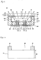
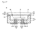
- Fig. 2 is a cross-sectional view of a light emitting apparatus according to a first embodiment of the present invention. Arrows in Fig. 2 indicate the forward direction of light emitted by a light emitting device 15.
- the light emitting apparatus 10 includes: a light emitting device accommodating body 11, an insulating film 12, a wiring pattern 13, a light emitting device 15, a light transmitting substrate 16 and a phosphor-containing, ultraviolet curing resin 17.
- the light emitting apparatus 10 is so designed that light having a desired color is provided after light emitted by the light emitting device 15 has passed through the phosphor-containing, ultraviolet curing resin 17.
- a light emitting diode that emits white light can be employed as the light emitting apparatus 10.
- a white light emitting diode is employed as the light emitting apparatus 10.
- the light emitting device accommodating body 11 includes a plate portion 18, a frame portion 19 and a recessed portion 20.
- the plate portion 18 is integrally formed with and supports the frame portion 19.
- a plurality of through holes 21 are formed in the plate portion 18, the thickness M1 of which is 200 ⁇ m, for example.
- the frame portion 19 is positioned on and integrally formed with the plate portion 18.
- the recessed portion 20 is defined by an upper face 18A of the plate portion 18 and an inner wall 19B of the frame portion 19, and is used to accommodate the light emitting device 15.
- the recessed portion 20 may be shaped, for example, like a cylinder or a quadrangular prism, and a depth D1 of this recessed portion 20 may be 200 ⁇ m, for example.
- the light emitting device accommodating body 11 may, for example, be made of silicon.
- the insulating film 12 is deposited to cover the surface (including the walls of the through holes 21) of the light emitting device accommodating body 11.
- the insulating film 12 is used to insulate the light emitting device accommodating body 11 from the wiring pattern 13.
- An oxide film for example, may be employed as the insulating film 12, which has a thickness, for example, of 1 ⁇ m.
- the insulating film 12 must be deposited so as to cover, at the least, a lower face 18B of the plate portion 18 and the walls of the through holes 21 in the light emitting device accommodating body 11.
- the wiring pattern 13 includes vias 23 and wires 24.
- the vias 23 are located in the through holes 21 in which the insulating film 21 is deposited.
- the upper ends of the vias 23 are electrically connected to the light emitting device 15, and the lower ends are connected to the wires 24.
- a conductive metal can be used as the material for the vias 23; as an example, Cu, specifically, can be employed.
- the wires 24 are provided on the lower face 18B of the plate portion 18 on which the insulating film 12 is formed, and the wires 24 are connected to the lower ends of the vias 23.
- the wires 24 are electrically connected by the vias 23 to the light emitting device 15, and serve as the external connection terminals of the light emitting apparatus 10.
- a conductive metal can be used as the material for the wires 24; as an example, specifically, an Ni/An film, which is obtained by laminating an Ni layer and an Au layer on the insulating film 12 in the named order, can be employed.
- the light emitting device 15 is accommodated in the recessed portion 20 of the light emitting device accommodating body 11.
- the light emitting device 15 is a device that emits light of a predetermined color, and includes electrodes 26. Since these electrodes 26 are electrically connected to the vias 23 at bumps 27, the light emitting device 15 is electrically connected to the wiring pattern 13.
- a blue LED light emitting diode
- the light transmitting substrate 16 is located on the light emitting device accommodating body 11, visible through the phosphor-containing, ultraviolet curing resin 17.
- the light transmitting substrate 16 is used to transmit light emitted by the light emitting device 15 and also to tightly close the recessed portion 20.
- a glass substrate, for example, may be employed as the light transmitting substrate 16.
- the phosphor-containing, ultraviolet curing resin 17 is arranged so as to cover a face 16A of the light transmitting substrate 16 opposite to the light emitting device accommodating body 11.
- the phosphor-containing, ultraviolet curing resin 17 contacts the insulating film 12 deposited on an upper face 19 of the frame portion 19.
- the phosphor-containing ultraviolet curing resin 17 is a material wherein phosphor particles 28 are dispersed in an ultraviolet curing resin 29, and when the light emitting apparatus 18 is to emit white light, particles of a yellow emitting phosphor need only be employed as the phosphor particles 28.
- yellow emitting phosphor a YAG phosphor, can be employed.
- the ultraviolet curing resin 29 is a resin that is cured using ultraviolet irradiation, and serves as an adhesive material.
- the ultraviolet curing resin 29 includes, for example, a base resin, a photo polymerization initiator and a thermosetting catalyst.
- An epoxy resin or an acrylic resin, for example, can be employed as a base resin; benzoin ether (specifically, for example, benzoin isopropyl ether) can be employed as a photo polymerization initiator; and an amine catalyst (specifically, diamine or polyamine, for example) can be employed as a thermosetting catalyst.
- the phosphor-containing, ultraviolet curing resin 17 covers the face 16A of the light transmitting substrate 16 opposite to the light emitting device accommodating body 11, and light emitted by the light emitting device 15 always passes through the phosphor-containing, ultraviolet curing resin 17, the chromaticity of the light emitting apparatus 10 can be improved.
- the phosphor-containing, ultraviolet curing resin 17 that serves as an adhesive material is located between the light emitting device accommodating body 11 and the light transmitting substrate 16, the light emitting device accommodating body 11 and the light transmitting substrate 16 can be adhered to each other, and thus, no adhesive material is required to bond these components. Therefore, the manufacturing costs for the light emitting apparatus 11 can be reduced.
- the phosphor-containing, ultraviolet curing resin 17 can be deposited, for example, by using squeegee printing, spin coating, a dispensing method, offset printing or inkjet printing.
- a thickness M2 of the phosphor-containing, ultraviolet curing resin 17 depends on desired luminance and chromaticity, and is, for example, 50 ⁇ m.
- chromaticity of this light emitting apparatus 10 can be increased by forming the phosphor-containing, ultraviolet curing resin 17 so that it covers the face 16A of the light transmitting substrate 16 opposite to the light emitting device accommodating body 11.
- the phosphor-containing, ultraviolet curing resin 17 is arranged between the light emitting device accommodating body 11 and the light transmitting substrate 16 to bond these two components, an adhesive material for adhering them to each other is not required, and the manufacturing costs of the light emitting apparatus 10 can be reduced.
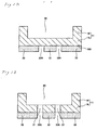
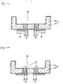
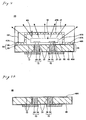
- Figs. 3A to 3P are diagrams showing the light emitting apparatus manufacturing processing according to the first embodiment of the invention.
- the same reference numerals as are used for the light emitting apparatus 10 are employed to denote identical or corresponding portions.
- a resist film 32 having an opening 32A, is formed on a base material 31.
- the opening 32A exposes the base material 31 and corresponds to the formation position of a recessed portion 20.
- the base material 31 can, for example, be silicon.
- a thickness M3 of the base material 31 is, for example, 400 ⁇ m, and the resist film 32 is, for example, a dry film resist.
- the base material 31 is etched by employing anisotropic etching that uses the resist film 32 as a mask, and the recessed portion 20 is formed.
- a light emitting device accommodating body 11 having a plate portion 18 and a frame portion 19 is obtained.
- a thickness M1 of the plate portion 18 is, for example, 200 ⁇ m
- a depth D1 of the recessed portion 20 is, for example, 200 ⁇ m.
- a dry etching method for example, is employed for anisotropic etching.
- a resist film 33 in which there are openings 33A, is deposited on a lower face 18B of the plate portion 18.
- the openings 33A expose the lower face 18B of the plate portion 18 and correspond to the formation positions of through holes 21.
- the resist film 33 may be, for example, a dry film resist.
- the plate portion 18 is etched by anisotropic etching using the resist film 33 as a mask, and the through holes 21 are formed.
- a dry etching method for example, is employed for anisotropic etching.
- the resist film 33 is removed, so that the light emitting device accommodating body 11 is obtained.
- an insulating film 12 is deposited so as to cover the surface (including the walls of the through holes 21) of the light emitting device accommodating body 11.
- the light emitting device accommodating body 11 is thermally oxidized.
- metal foil 35 is glued to the lower face of the resultant structure shown in Fig. 3G. Thereafter, electrolytic plating is performed using the metal foil 35 as a power supply layer, and a metal film is grown through precipitation so as to fill the through holes 21. In this manner, the vias 23 are obtained.
- Cu foil for example, is employed as the metal foil 35, and a Cu film, for example, is employed as a metal film that fills the through holes 21.
- the metal foil 35 is glued through a dry film to the lower face of the resultant structure, and portions of the dry film corresponding to the vias 23 are removed by a developing solution which is inlet from the vias 23.
- a metal film 36 is formed to cover the lower face of the structure shown in Fig. 3I.
- the metal film 36 is to be patterned, using a process in Fig. 3L, and serve as wires 24.
- An Ni/Au film obtained by laminating an Ni layer and Au layer, in the named order, on the insulating film 12, for example, is employed as the insulating film 36.
- a sputtering method, for example, can be employed to deposit the metal film 36.
- a patterned resist film 38 is formed on a face 36A of the metal film 36.
- the metal film 36 is etched until the insulating film 12 is exposed and the wires 24 are obtained.
- the wiring pattern which includes the vias 23 and the wires 24, is obtained.
- the resist film 38 is removed, and bumps 27 are formed at the upper ends of the vias 23.
- Au bumps for example, can be employed as the bumps 27.
- the electrodes 26 of the light emitting device 15 are connected to the welded bumps 27, so that the light emitting device 15 and the wiring pattern 13 are electrically connected.
- phosphor-containing, ultraviolet curing resin 17 is formed to cover the face 16A of the light transmitting substrate 16 opposite to the light emitting device accommodating body 11 (phosphor-containing resin formation step).
- the phosphor-containing, ultraviolet curing resin 17 has not yet been cured.
- the phosphor-containing, ultraviolet curing resin 17 is a material wherein phosphor particles 28 are dispersed in an ultraviolet curing resin 29.
- particles of a yellow emitting phosphor can be employed as the phosphor particles 28.
- a YAG phosphor can be employed.
- the ultraviolet curing resin 29 is a resin that is cured by ultraviolet irradiation, and serves as an adhesive material.
- the ultraviolet curing resin 29 is made, for example, of a base resin, a photo polymerization initiator and a thermosetting catalyst.
- An epoxy resin or an acrylic resin, for example, can be employed as a base resin; benzoin ether (specifically, for example, benzoin isopropyl ether) can be employed as a photo polymerization initiator; and an amine catalyst (specifically, for example, diamine or polyamine) can be employed as a thermosetting catalyst.
- the phosphor-containing, ultraviolet curing resin 17 can be deposited, for example, by using squeegee printing, spin coating, adispensingmethod, offset printing or inkjet printing.
- a thickness M2 of the phosphor-containing, ultraviolet curing resin 17 depends on desired luminance and chromaticity, and is, for example, 50 ⁇ m.
- the phosphor-containing, ultraviolet curing resin 17, formed on the structure in Fig. 30, is brought into contact with the top of the structure in Fig. 3N (specifically, the top of the frame portion 19 whereat the insulating film 12 is deposited). Thereafter, the phosphor-containing, ultraviolet curing resin 17 is cured using ultraviolet irradiation, and the light emitting device accommodating body 11 and the light transmitting substrate 16 are adhered to each other (phosphor-containing resin curing step). Specifically, ultraviolet rays having a wavelength of 200 to 400 nm are emitted at a radiant exposure of 2000 mJ/cm 2 to cure the phosphor-containing, ultraviolet curing resin 17.
- the phosphor-containing, ultraviolet curing resin 17, provided for the light transmitting substrate 16 is brought into contact with the insulating film 12, deposited on the upper face 19A of the frame portion 19. Thereafter, the phosphor-containing, ultraviolet curing resin 17 is cured using ultraviolet irradiation, and the light emitting device accommodating body 11 and the light transmitting substrate 16 are adhered to each other.
- an adhesive material is not required, and the manufacturing costs of the light emitting apparatus can be reduced.
- a white light emitting diode is employed as the light emitting apparatus 10.
- this embodiment can be also applied for a light emitting apparatus that emits light of other colors.
- a plurality of ultraviolet curing resin layers containing phosphors that emit different colors may be provided on the face 16A of the light transmitting substrate 16 opposite to the light emitting device accommodating body 11. Also in this case, the same effects as in the embodiment can be obtained.
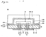
- Fig. 4 is a cross-sectional view of a light emitting apparatus according to a second embodiment of the present invention. Arrows in Fig. 4 indicate the forward direction of light emitted by a light emitting device 15. In Fig. 4, the same reference numerals as are used for the light emitting apparatus 10 in the first embodiment are provided for identical or corresponding portions.
- the light emitting apparatus 45 includes: a light emitting device 15, a substrate 46, a light transmitting member 47 and a phosphor-containing, ultraviolet curing resin 54.
- the light emitting apparatus 45 is designed so that light of a desired color is obtained after light emitted by the light emitting device 15 has passed through the phosphor-containing, ultraviolet curing resin 54.
- a white light emitting diode for example, can be employed as the light emitting apparatus 45. In the explanation for this embodiment, a white light emitting diode is employed as the light emitting apparatus 45.
- the substrate 46 includes a substrate body 49, an insulating film 12 and wiring patterns, each of which is formed of a via 23 and a wire 24.
- the substrate body 49 is plate shaped, and through holes 51 are formed in the substrate body 49 in order to arrange the vias 23.
- the material used for the substrate body 49 is, for example, silicon.
- the insulating film 12 is deposited to cover the surface (including the walls of the through holes 51) of the substrate body 49.
- the vias 23 are arranged in the through holes 51, along which the insulating film 12 is formed.
- the wires 24 are formed on a lower face 49A of the substrate body 49,. on which the insulating film 12 is deposited, and are connected to the lower ends of the vias 23.
- the light transmitting member 47 is mounted on the substrate 46, using the phosphor-containing, ultraviolet curing resin 54, and has a recessed portion 55 that accommodates the light emitting device 15.
- the recessed portion 15 may be shaped, for example, like a cylinder or a quadrangular prism, and a depth D2 may be, for example, 200 ⁇ m.
- the light transmitting member 47 is a member that permits the transmission of light emitted by the light emitting device 15, and that encloses the upper face and the side faces of the light emitting device 15.
- a glass substrate, for example, can be employed as the light transmitting member 47.
- the phosphor-containing ultraviolet curing resin 54 is provided to cover a face 47A of the light transmitting member 47, which is opposite to an upper face 46A of the substrate 46, and a face 47B of the light transmitting member 47, which corresponds to the recessed portion 55.
- the ultraviolet curing resin 29 is to be cured using ultraviolet irradiation and serves as an adhesive material.
- the phosphor-containing, ultraviolet curing resin 54 is provided to cover the face 47A of the light transmitting member 47 opposite to the substrate 46 and the face 47B of the light transmitting member 47, corresponding to the recessed portion 55, light emitted by the light emitting device 15 always passes through the phosphor-containing, ultraviolet curing resin 54. Therefore, the chromaticity of the light emitting apparatus 45 can be improved.
- the phosphor-containing, ultraviolet curing resin 54 that serves as an adhesive material is provided between the light transmitting member 47 and the upper face 46A of the substrate 46, the substrate 46 and the light transmitting member 47 can be bonded together. Thus, anadhesive material for bonding these two components is not required, and the manufacturing costs of the light emitting apparatus can be reduced.
- the phosphor-containing, ultraviolet curing resin 54 can be deposited, for example, by using spin coating, a dispensing method, offset printing or inkjet printing.
- a thickness M4 of the phosphor-containing, ultraviolet curing resin 54 depends on the desired luminance and chromaticity values, but is, for example, 50 ⁇ m.
- the phosphor-containing, ultraviolet curing resin 54 is formed to cover the face 47A of the light transmitting member 47 opposite to the substrate 46, and the face 47B of the light transmitting member 47 corresponding to the recessed portion 55, the chromaticity of the light emitting apparatus 45 can be improved.
- the manufacturing costs of the light emitting apparatus can be reduced.
- Figs. 5A to 5D are diagrams showing the processing for the second embodiment for manufacturing a light emitting apparatus.
- the same reference numerals as are used for the light emitting apparatus 45 of the second embodiment are provided for identical or corresponding portions.
- a substrate 46 is formed by performing the processes in Figs. 3D to 3L, explained in the first embodiment. Then, in a process in Fig. 5B, for the processes in Figs. 3M and 3N explained in the first embodiment, a light emitting device 15 is electrically connected to wiring patterns 13 mounted on the substrate 46.
- aphosphor-containing, ultraviolet curing resin 54 is formed to cover a face 47A of a light transmitting member 47 opposite to the substrate 46, and a face 47B, of the light transmitting member 47, corresponding to a recessed portion 55 (a phosphor-containing resin formation step). At this time, the phosphor-containing, ultraviolet curing resin 54 has not yet been cured.
- the light transmitting member 47 on which the phosphor-containing, ultraviolet curing resin 54 is deposited is brought into contact with an upper face 46A of the substrate 46. Thereafter, the phosphor-containing, ultraviolet curing resin 54 is cured by using ultraviolet irradiation, and the substrate 46 and the light transmitting member 47 are bonded together (a phosphor-containing resin curing step). Specifically, ultraviolet rays having a wavelength of 200 to 400 nm are emitted at a radiant exposure of 2000 mJ/cm 2 to cure the phosphor-containing, ultraviolet curing resin 54.
- the light transmitting member on which the phosphor-containing, ultraviolet curing resin 54 is deposited is brought into contact with the upper face 46A of the substrate 46, and thereafter, using ultraviolet irradiation, the phosphor-containing, ultraviolet curing resin 54 is cured so that the substrate and the light transmitting member 47 adhere to each other.
- no adhesive material is required to bond together the substrate 46 and the light transmitting member 47, and the manufacturing costs of the light emitting apparatus 45 can be reduced.
- a white light emitting diode is employed as the light emitting apparatus 45.
- this embodiment can also be applied for a light emitting apparatus that emits a light of another color.
- a plurality of ultraviolet curing resin layers that contain phosphors and that emit different colors may be provided on the face 47A of the light transmitting member 47, opposite to the substrate 46 and the face 47B of the light transmitting member 47, corresponding to the recessed portion 55. In this case, the same effects as in the second embodiment can be obtained.
- phosphors are contained in the ultraviolet curing resin layers, for example, by about 10 to 70wt%.
- Fig. 5E is a cross-sectional view of a light emitting apparatus according to a modification of the second embodiment. Arrows in Fig. 5E indicate the forward direction of light emitted by a light emitting device 15. In Fig. 5E, the same reference numerals as are used for the light emitting apparatus 45 in the second embodiment are employed to denote identical or corresponding portions.
- a light emitting apparatus 60 has the same arrangement as the light emitting apparatus 45, except that a light emitting member 61 having a hemispherical (dome shaped) recessed portion 62 is provided, instead of the light transmitting member 47 of the light emitting apparatus 45 in the second embodiment, and that a phosphor-containing, ultraviolet curing resin 54 is formed to cover a face 61A of the light transmittingmember 61, which is opposite to a substrate 46, and a face 61B of the light transmitting member 61, which corresponds to the recessed portion 62.
- the same effects can be acquired as are provided by the light emitting apparatus 45 of the second embodiment. It should be noted that the light emitting apparatus 60 can be provided by the employing the same method as is used for the light emitting apparatus 45 of the second embodiment.
- the present invention can be applied for a light emitting apparatus, for which the chromaticity can be improved and the manufacturing costs can be reduced, and a manufacturing method therefor.
Landscapes
- Led Device Packages (AREA)
Applications Claiming Priority (1)
| Application Number | Priority Date | Filing Date | Title |
|---|---|---|---|
| JP2005378415A JP4828226B2 (ja) | 2005-12-28 | 2005-12-28 | 発光装置及びその製造方法 |
Publications (3)
| Publication Number | Publication Date |
|---|---|
| EP1804304A2 true EP1804304A2 (fr) | 2007-07-04 |
| EP1804304A3 EP1804304A3 (fr) | 2013-01-09 |
| EP1804304B1 EP1804304B1 (fr) | 2017-05-17 |
Family
ID=37882119
Family Applications (1)
| Application Number | Title | Priority Date | Filing Date |
|---|---|---|---|
| EP06027021.2A Ceased EP1804304B1 (fr) | 2005-12-28 | 2006-12-28 | Appareil à luminescence et procédé de sa fabrication |
Country Status (5)
| Country | Link |
|---|---|
| US (1) | US7876036B2 (fr) |
| EP (1) | EP1804304B1 (fr) |
| JP (1) | JP4828226B2 (fr) |
| KR (1) | KR20070070096A (fr) |
| TW (1) | TW200733433A (fr) |
Cited By (8)
| Publication number | Priority date | Publication date | Assignee | Title |
|---|---|---|---|---|
| WO2009039816A1 (fr) * | 2007-09-27 | 2009-04-02 | Osram Opto Semiconductors Gmbh | Élément rayonnant doté d'un couvercle de verre et procédé de fabrication |
| EP2071636A1 (fr) * | 2007-12-14 | 2009-06-17 | Cree, Inc. | Distribution de phosphore dans des lampes DEL utilisant la force centrifuge |
| WO2013167399A1 (fr) * | 2012-05-11 | 2013-11-14 | Osram Opto Semiconductors Gmbh | Composant optoélectronique et procédé de fabrication d'un composant optoélectronique |
| US9041285B2 (en) | 2007-12-14 | 2015-05-26 | Cree, Inc. | Phosphor distribution in LED lamps using centrifugal force |
| US9093616B2 (en) | 2003-09-18 | 2015-07-28 | Cree, Inc. | Molded chip fabrication method and apparatus |
| US9159888B2 (en) | 2007-01-22 | 2015-10-13 | Cree, Inc. | Wafer level phosphor coating method and devices fabricated utilizing method |
| US9166126B2 (en) | 2011-01-31 | 2015-10-20 | Cree, Inc. | Conformally coated light emitting devices and methods for providing the same |
| US10546846B2 (en) | 2010-07-23 | 2020-01-28 | Cree, Inc. | Light transmission control for masking appearance of solid state light sources |
Families Citing this family (15)
| Publication number | Priority date | Publication date | Assignee | Title |
|---|---|---|---|---|
| KR100950491B1 (ko) | 2006-08-03 | 2010-03-31 | 삼성전자주식회사 | 네트워크 인터페이스카드, 이를 갖는 네트워크프린터 및 그 장치의 제어방법 |
| CN100483762C (zh) * | 2008-02-25 | 2009-04-29 | 鹤山丽得电子实业有限公司 | 一种发光二极管器件的制造方法 |
| CN101257075B (zh) * | 2008-03-13 | 2010-05-12 | 鹤山丽得电子实业有限公司 | 一种发光二极管器件及其制造方法 |
| JP2010045248A (ja) * | 2008-08-14 | 2010-02-25 | Citizen Electronics Co Ltd | 発光ダイオード |
| WO2010123059A1 (fr) * | 2009-04-22 | 2010-10-28 | シーシーエス株式会社 | Procédé de fabrication de dispositif émettant de la lumière à del |
| US9456508B2 (en) * | 2010-05-28 | 2016-09-27 | Apple Inc. | Methods for assembling electronic devices by internally curing light-sensitive adhesive |
| KR20140075640A (ko) * | 2010-11-10 | 2014-06-19 | 쿠오-쿠앙 창 | 덮개판의 제조방법 및 덮개판을 사용하여 발광 다이오드 패키지를 제조하기 위한 방법 |
| EP3716331B1 (fr) * | 2010-12-28 | 2023-06-28 | Nichia Corporation | Dispositif électroluminescent |
| JP5863291B2 (ja) * | 2011-06-28 | 2016-02-16 | 株式会社小糸製作所 | 平面発光モジュール |
| US9172057B2 (en) * | 2011-06-30 | 2015-10-27 | Osram Oled Gmbh | Encapsulation structure for an opto-electronic component |
| KR101434835B1 (ko) * | 2012-10-29 | 2014-09-02 | 연세대학교 산학협력단 | 발광 효율을 개선할 수 있는 구조를 갖는 led 패키지 및 그 제조방법 |
| CN105140377A (zh) * | 2015-08-10 | 2015-12-09 | 深圳市华星光电技术有限公司 | 量子点玻璃盒及其制备方法和应用 |
| JP6387954B2 (ja) * | 2015-12-24 | 2018-09-12 | 日亜化学工業株式会社 | 波長変換部材を用いた発光装置の製造方法 |
| US11532771B2 (en) | 2018-03-13 | 2022-12-20 | Suzhou Lekin Semiconductor Co., Ltd. | Semiconductor device package |
| KR102509089B1 (ko) * | 2018-03-13 | 2023-03-10 | 쑤저우 레킨 세미컨덕터 컴퍼니 리미티드 | 반도체 소자 패키지 |
Family Cites Families (14)
| Publication number | Priority date | Publication date | Assignee | Title |
|---|---|---|---|---|
| JP2000031548A (ja) * | 1998-07-09 | 2000-01-28 | Stanley Electric Co Ltd | 面実装型発光ダイオードおよびその製造方法 |
| DE10023353A1 (de) * | 2000-05-12 | 2001-11-29 | Osram Opto Semiconductors Gmbh | Optoelektronisches Bauelement und Verfahren zur Herstellung |
| JP4061869B2 (ja) * | 2001-07-26 | 2008-03-19 | 松下電工株式会社 | 発光装置の製造方法 |
| JP2003110146A (ja) | 2001-07-26 | 2003-04-11 | Matsushita Electric Works Ltd | 発光装置 |
| TW552726B (en) * | 2001-07-26 | 2003-09-11 | Matsushita Electric Works Ltd | Light emitting device in use of LED |
| JP3749243B2 (ja) * | 2001-09-03 | 2006-02-22 | 松下電器産業株式会社 | 半導体発光デバイス,発光装置及び半導体発光デバイスの製造方法 |
| JP3948650B2 (ja) * | 2001-10-09 | 2007-07-25 | アバゴ・テクノロジーズ・イーシービーユー・アイピー(シンガポール)プライベート・リミテッド | 発光ダイオード及びその製造方法 |
| JP2004140185A (ja) * | 2002-10-17 | 2004-05-13 | Matsushita Electric Ind Co Ltd | 発光装置 |
| JP4254276B2 (ja) * | 2003-03-03 | 2009-04-15 | 豊田合成株式会社 | 発光装置およびその製造方法 |
| JP2004349646A (ja) * | 2003-05-26 | 2004-12-09 | Matsushita Electric Works Ltd | 発光装置 |
| JP2005259847A (ja) * | 2004-03-10 | 2005-09-22 | Nitto Denko Corp | 光半導体装置の製造方法 |
| JP4543712B2 (ja) * | 2004-03-17 | 2010-09-15 | 日亜化学工業株式会社 | 発光装置の製造方法 |
| JP5081370B2 (ja) * | 2004-08-31 | 2012-11-28 | 日亜化学工業株式会社 | 発光装置 |
| JP2006135225A (ja) * | 2004-11-09 | 2006-05-25 | Toshiba Corp | 発光装置 |
-
2005
- 2005-12-28 JP JP2005378415A patent/JP4828226B2/ja not_active Expired - Fee Related
-
2006
- 2006-12-27 KR KR20060134770A patent/KR20070070096A/ko not_active Withdrawn
- 2006-12-27 US US11/645,581 patent/US7876036B2/en not_active Expired - Fee Related
- 2006-12-28 TW TW095149424A patent/TW200733433A/zh unknown
- 2006-12-28 EP EP06027021.2A patent/EP1804304B1/fr not_active Ceased
Cited By (14)
| Publication number | Priority date | Publication date | Assignee | Title |
|---|---|---|---|---|
| US10164158B2 (en) | 2003-09-18 | 2018-12-25 | Cree, Inc. | Molded chip fabrication method and apparatus |
| US10546978B2 (en) | 2003-09-18 | 2020-01-28 | Cree, Inc. | Molded chip fabrication method and apparatus |
| US9093616B2 (en) | 2003-09-18 | 2015-07-28 | Cree, Inc. | Molded chip fabrication method and apparatus |
| US9105817B2 (en) | 2003-09-18 | 2015-08-11 | Cree, Inc. | Molded chip fabrication method and apparatus |
| US9159888B2 (en) | 2007-01-22 | 2015-10-13 | Cree, Inc. | Wafer level phosphor coating method and devices fabricated utilizing method |
| WO2009039816A1 (fr) * | 2007-09-27 | 2009-04-02 | Osram Opto Semiconductors Gmbh | Élément rayonnant doté d'un couvercle de verre et procédé de fabrication |
| EP2071636A1 (fr) * | 2007-12-14 | 2009-06-17 | Cree, Inc. | Distribution de phosphore dans des lampes DEL utilisant la force centrifuge |
| US8167674B2 (en) | 2007-12-14 | 2012-05-01 | Cree, Inc. | Phosphor distribution in LED lamps using centrifugal force |
| US9041285B2 (en) | 2007-12-14 | 2015-05-26 | Cree, Inc. | Phosphor distribution in LED lamps using centrifugal force |
| US10546846B2 (en) | 2010-07-23 | 2020-01-28 | Cree, Inc. | Light transmission control for masking appearance of solid state light sources |
| US9166126B2 (en) | 2011-01-31 | 2015-10-20 | Cree, Inc. | Conformally coated light emitting devices and methods for providing the same |
| US9515242B2 (en) | 2012-05-11 | 2016-12-06 | Osram Oled Gmbh | Optoelectronic component and method for producing an optoelectronic component |
| US20150115304A1 (en) * | 2012-05-11 | 2015-04-30 | Osram Opto Semiconductors Gmbh | Optoelectronic component and method for producing an optoelectronic component |
| WO2013167399A1 (fr) * | 2012-05-11 | 2013-11-14 | Osram Opto Semiconductors Gmbh | Composant optoélectronique et procédé de fabrication d'un composant optoélectronique |
Also Published As
| Publication number | Publication date |
|---|---|
| TW200733433A (en) | 2007-09-01 |
| US20070182307A1 (en) | 2007-08-09 |
| JP4828226B2 (ja) | 2011-11-30 |
| US7876036B2 (en) | 2011-01-25 |
| EP1804304B1 (fr) | 2017-05-17 |
| JP2007180347A (ja) | 2007-07-12 |
| KR20070070096A (ko) | 2007-07-03 |
| EP1804304A3 (fr) | 2013-01-09 |
Similar Documents
| Publication | Publication Date | Title |
|---|---|---|
| EP1804304B1 (fr) | Appareil à luminescence et procédé de sa fabrication | |
| US20200243739A1 (en) | Board connection structure, board mounting method, and micro-led display | |
| KR101162404B1 (ko) | 수지 밀봉 발광체 및 그 제조 방법 | |
| JP5323501B2 (ja) | 発光ダイオードパッケージ及びその製造方法 | |
| CN103227263B (zh) | 配线基板及配线基板的制造方法 | |
| US20210119098A1 (en) | Substrate mounting method and electronic-component-mounted substrate | |
| WO2019111610A1 (fr) | Procédé de production de panneau d'affichage à del | |
| KR101911707B1 (ko) | 배선 기판 및 배선 기판의 제조 방법 | |
| US7708613B2 (en) | Method of producing light emitting apparatus | |
| KR20120061376A (ko) | 반도체 발광 소자에 형광체를 도포하는 방법 | |
| JP2009033088A (ja) | 半導体発光装置、その製造方法およびそれを用いたled照明装置 | |
| US9590154B2 (en) | Wiring substrate and light emitting device | |
| JP2020013954A (ja) | 基板接続構造、マイクロledディスプレイ及び部品実装方法 | |
| CN104620400A (zh) | Led封装及其制造方法 | |
| TW202114251A (zh) | 電子零件封裝構造、電子零件封裝方法及led顯示面板 | |
| US20070161316A1 (en) | Method of manufacturing light emitting apparatus | |
| JP2021056386A (ja) | Led表示装置の製造方法及びled表示装置 | |
| JP2008159705A (ja) | 発光装置 | |
| WO2020003869A1 (fr) | Procédé de montage de carte et carte de montage de composants électroniques | |
| KR101460742B1 (ko) | 반도체 소자 구조물을 제조하는 방법 | |
| KR102901591B1 (ko) | 단자가 상부로 형성되는 소자를 포함하는 표시패널 및 이의 제조방법 | |
| CN114628566B (zh) | 光色转换结构、发光单元及发光单元制作方法 | |
| EP1856733A2 (fr) | Procédé de micro-emballage de del et micro-emballage | |
| CN103928598A (zh) | 具有厚膜环绕壁的发光二极管元件基板、元件及制法 | |
| JP2009099590A (ja) | Ledディスプレーの製造方法 |
Legal Events
| Date | Code | Title | Description |
|---|---|---|---|
| PUAI | Public reference made under article 153(3) epc to a published international application that has entered the european phase |
Free format text: ORIGINAL CODE: 0009012 |
|
| AK | Designated contracting states |
Kind code of ref document: A2 Designated state(s): AT BE BG CH CY CZ DE DK EE ES FI FR GB GR HU IE IS IT LI LT LU LV MC NL PL PT RO SE SI SK TR |
|
| AX | Request for extension of the european patent |
Extension state: AL BA HR MK YU |
|
| RIN1 | Information on inventor provided before grant (corrected) |
Inventor name: TAGUCHI, YUICHI Inventor name: KOIZUMI, NAOYUKI Inventor name: SUNOHARA, MASAHIRO Inventor name: MURAYAMA, KEI Inventor name: SAKAGUCHI, HIDEAKI Inventor name: SHIRAISHI, AKINORI Inventor name: HIGASHI, MITSUTOSHI |
|
| PUAL | Search report despatched |
Free format text: ORIGINAL CODE: 0009013 |
|
| AK | Designated contracting states |
Kind code of ref document: A3 Designated state(s): AT BE BG CH CY CZ DE DK EE ES FI FR GB GR HU IE IS IT LI LT LU LV MC NL PL PT RO SE SI SK TR |
|
| AX | Request for extension of the european patent |
Extension state: AL BA HR MK RS |
|
| RIC1 | Information provided on ipc code assigned before grant |
Ipc: H01L 33/00 20100101AFI20121203BHEP Ipc: H01L 33/50 20100101ALI20121203BHEP |
|
| 17P | Request for examination filed |
Effective date: 20130704 |
|
| RBV | Designated contracting states (corrected) |
Designated state(s): AT BE BG CH CY CZ DE DK EE ES FI FR GB GR HU IE IS IT LI LT LU LV MC NL PL PT RO SE SI SK TR |
|
| AKX | Designation fees paid |
Designated state(s): DE |
|
| GRAP | Despatch of communication of intention to grant a patent |
Free format text: ORIGINAL CODE: EPIDOSNIGR1 |
|
| RIC1 | Information provided on ipc code assigned before grant |
Ipc: H01L 33/00 20100101AFI20161128BHEP Ipc: H01L 33/50 20100101ALI20161128BHEP Ipc: H01L 33/48 20100101ALN20161128BHEP |
|
| INTG | Intention to grant announced |
Effective date: 20161212 |
|
| GRAS | Grant fee paid |
Free format text: ORIGINAL CODE: EPIDOSNIGR3 |
|
| GRAA | (expected) grant |
Free format text: ORIGINAL CODE: 0009210 |
|
| AK | Designated contracting states |
Kind code of ref document: B1 Designated state(s): DE |
|
| REG | Reference to a national code |
Ref country code: DE Ref legal event code: R096 Ref document number: 602006052552 Country of ref document: DE |
|
| REG | Reference to a national code |
Ref country code: DE Ref legal event code: R097 Ref document number: 602006052552 Country of ref document: DE |
|
| PLBE | No opposition filed within time limit |
Free format text: ORIGINAL CODE: 0009261 |
|
| STAA | Information on the status of an ep patent application or granted ep patent |
Free format text: STATUS: NO OPPOSITION FILED WITHIN TIME LIMIT |
|
| 26N | No opposition filed |
Effective date: 20180220 |
|
| PGFP | Annual fee paid to national office [announced via postgrant information from national office to epo] |
Ref country code: DE Payment date: 20201216 Year of fee payment: 15 |
|
| REG | Reference to a national code |
Ref country code: DE Ref legal event code: R119 Ref document number: 602006052552 Country of ref document: DE |
|
| PG25 | Lapsed in a contracting state [announced via postgrant information from national office to epo] |
Ref country code: DE Free format text: LAPSE BECAUSE OF NON-PAYMENT OF DUE FEES Effective date: 20220701 |