EP1805904B1 - Kodierung von rfid - Google Patents
Kodierung von rfid Download PDFInfo
- Publication number
- EP1805904B1 EP1805904B1 EP05792425A EP05792425A EP1805904B1 EP 1805904 B1 EP1805904 B1 EP 1805904B1 EP 05792425 A EP05792425 A EP 05792425A EP 05792425 A EP05792425 A EP 05792425A EP 1805904 B1 EP1805904 B1 EP 1805904B1
- Authority
- EP
- European Patent Office
- Prior art keywords
- signals
- signal
- branches
- child
- mother
- Prior art date
- Legal status (The legal status is an assumption and is not a legal conclusion. Google has not performed a legal analysis and makes no representation as to the accuracy of the status listed.)
- Expired - Lifetime
Links
Images

Classifications
-
- G—PHYSICS
- G06—COMPUTING OR CALCULATING; COUNTING
- G06K—GRAPHICAL DATA READING; PRESENTATION OF DATA; RECORD CARRIERS; HANDLING RECORD CARRIERS
- G06K19/00—Record carriers for use with machines and with at least a part designed to carry digital markings
- G06K19/06—Record carriers for use with machines and with at least a part designed to carry digital markings characterised by the kind of the digital marking, e.g. shape, nature, code
- G06K19/067—Record carriers with conductive marks, printed circuits or semiconductor circuit elements, e.g. credit or identity cards also with resonating or responding marks without active components
-
- G—PHYSICS
- G06—COMPUTING OR CALCULATING; COUNTING
- G06K—GRAPHICAL DATA READING; PRESENTATION OF DATA; RECORD CARRIERS; HANDLING RECORD CARRIERS
- G06K7/00—Methods or arrangements for sensing record carriers, e.g. for reading patterns
-
- G—PHYSICS
- G06—COMPUTING OR CALCULATING; COUNTING
- G06K—GRAPHICAL DATA READING; PRESENTATION OF DATA; RECORD CARRIERS; HANDLING RECORD CARRIERS
- G06K19/00—Record carriers for use with machines and with at least a part designed to carry digital markings
- G06K19/06—Record carriers for use with machines and with at least a part designed to carry digital markings characterised by the kind of the digital marking, e.g. shape, nature, code
- G06K19/067—Record carriers with conductive marks, printed circuits or semiconductor circuit elements, e.g. credit or identity cards also with resonating or responding marks without active components
- G06K19/0672—Record carriers with conductive marks, printed circuits or semiconductor circuit elements, e.g. credit or identity cards also with resonating or responding marks without active components with resonating marks
- G06K19/0675—Record carriers with conductive marks, printed circuits or semiconductor circuit elements, e.g. credit or identity cards also with resonating or responding marks without active components with resonating marks the resonating marks being of the surface acoustic wave [SAW] kind
-
- G—PHYSICS
- G01—MEASURING; TESTING
- G01S—RADIO DIRECTION-FINDING; RADIO NAVIGATION; DETERMINING DISTANCE OR VELOCITY BY USE OF RADIO WAVES; LOCATING OR PRESENCE-DETECTING BY USE OF THE REFLECTION OR RERADIATION OF RADIO WAVES; ANALOGOUS ARRANGEMENTS USING OTHER WAVES
- G01S13/00—Systems using the reflection or reradiation of radio waves, e.g. radar systems; Analogous systems using reflection or reradiation of waves whose nature or wavelength is irrelevant or unspecified
- G01S13/74—Systems using reradiation of radio waves, e.g. secondary radar systems; Analogous systems
- G01S13/75—Systems using reradiation of radio waves, e.g. secondary radar systems; Analogous systems using transponders powered from received waves, e.g. using passive transponders, or using passive reflectors
- G01S13/751—Systems using reradiation of radio waves, e.g. secondary radar systems; Analogous systems using transponders powered from received waves, e.g. using passive transponders, or using passive reflectors wherein the responder or reflector radiates a coded signal
Definitions
- Bar codes are commonly used for identifying objects in shops and supermarkets.
- An application of magnetic strips is the credit card.
- the main reason for the popularity of barcodes and magnetic strips is that they are inexpensive.
- One drawback of barcodes and magnetic strips is the distance range in which they can be used.
- the reader has to have a physical contact or has to be very close, say a few centimetres. If there is no physical contact, then the space between the code and the reader should not have any obstruction. In addition, the reader and the code have to be properly aligned for correct readability. This demands concentration from the part of the human operator and therefore is inconvenient.
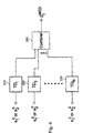
- Fig. 3 shows a general block diagram showing the generation of a signal string from a single child signal produced from a mother signal of one particular frequency containing an N bit data having the properties of either PSK (phase shift keying), ASK (amplitude shift keying) or PPM (pulse position modulation).
- Fig. 3 consists of an N way power divider 170 , N time-delays 110, 120, 130 , N phase shifters 112, 122, 132, N attenuators 114, 124, 134 , and an N way power combiner 180.
- the various signal string formats can be derived as follows.
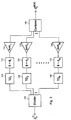
- the reflected signals from each branch 401, 402, 403, 404, 405, 406 therefore will pass through the reciprocal delays 410. 420, 430, 440, 450, 460, phase shifters 412, 422, 432, 442, 452, 462 and attenuators 414, 424, 434, 444, 454, 464 in the reverse direction and finally through block 470 , which acts like a combiner in the reverse direction.
- An example of block 470 in Fig. 6 is the Wilkinson's divider/combiner 470.
- the delayed signal reflected out at the point where the signal enters at block 470 A will have same property as in S 1 MOD of Fig. 5 if the values of the delays, attenuation and phase shifting in Fig. 6 are half that of Fig. 5 . Therefore the embodiment described in Fig. 6 will have same functionality as that of Fig. 5 with the additional advantage of reduced size.
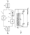
- the method described above can be used to construct an RFID-tag and a reader to decode the encoded RF waveform emitted by the RFID-tag.
- the RFID-tag can be considered as an interconnection of the following building blocks.
Landscapes
- Physics & Mathematics (AREA)
- Engineering & Computer Science (AREA)
- General Physics & Mathematics (AREA)
- Theoretical Computer Science (AREA)
- Acoustics & Sound (AREA)
- Artificial Intelligence (AREA)
- Computer Vision & Pattern Recognition (AREA)
- Near-Field Transmission Systems (AREA)
- Digital Transmission Methods That Use Modulated Carrier Waves (AREA)
- Radar Systems Or Details Thereof (AREA)
- Transmission Systems Not Characterized By The Medium Used For Transmission (AREA)
- Reduction Or Emphasis Of Bandwidth Of Signals (AREA)
Claims (9)
- Verfahren zum Erzeugen einer modulierten Wellenform in einem Funkfrequenzidentifizierungssystem, RFID-System, das K Signale aufweist, die als Hauptsignale Si m einer Dauer Ti m und Frequenzen Fi bezeichnet werden, wobei i=1...K und K≥1 ist, gekennzeichnet durch:- Erzeugen, aus den K Hauptsignalen, von K Zusatzsignalen einer Dauer Ti C, die als Untersignale Si C bezeichnet werden, wobei
 - Teilen jedes der Untersignale entsprechend jedem Hauptsignal mittels eines Leistungsteilers (170) in Ni Verzweigungen, wobei sich weitere Ni Untersignale ergeben, wobei Ni ≥ 2 ist;- Einführen von unterschiedlichen Verzögerungen TDi j bei den Ni Zusatz-Untersignalen nach der Leistungsteilung, wobei die Verzögerungen gemäß einem vorbestimmten Modulationsschema definiert werden, um entweder TDi j = jxTi C , wobei j=1... Ni ist, für die Phasenumtastung, Amplitudenumtastung und Frequenzumtastung zu sein, oder TDi j - TDi j-1 = tx, wobei j=2... Ni und tx = t 0 für eine binäre Null und tx = t 1 für eine binäre Eins mit t 0 ≠ t 1, für die Pulsphasenmodulation zu sein;- Bilden eines kombinierten Signals
 - im Fall der Phasenumtastung: Einführen der jeweiligen Phasenverschiebungen Θ j zum Festlegen der Phase von jedem der Zusatz-Untersignale, so dass sich die gesamte Phasenverschiebung bei denjenigen der Zusatz-Untersignale, die einen Bitwert von bj = 1 darstellen, in den kombinierten Signalen
 - im Fall der Amplitudenumtastung: Einführen von jeweiligen Dämpfungen Aj für jedes der Zusatz-Untersignale mit Aj = 0 zum Darstellen eines Bitwerts von bj = 1 in den kombinierten Signalen
 - im Fall der Frequenzumtastung: Kombinieren der Zusatz-Untersignale, die durch eine Zeitverzögerung TDi j verzögert werden; wobei die Zusatz-Untersignale

- Verfahren gemäß Anspruch 1, wobei das Erzeugen Folgendes aufweist:- Teilen eines Hauptsignals
 - Verzögern eines ersten Signals von den zwei Signalen mit einer ersten Zeitverzögerung;- Verzögern eines zweiten Signals von den zwei Signalen mit einer zweiten unterschiedlichen Zeitverzögerung;- Verschieben der Phase des zweiten Signals mit einem Winkel Φ°, wobei Φ so eingestellt wird, dass eine Phasendifferenz zwischen zwei Signalen 180° beträgt, wenn die Signale kombiniert werden; und- Bilden eines Untersignals
- Funkfrequenzidentifikations-tag, RFID-tag, mit einer Einrichtung zum Vorsehen der K Signale, die als Hauptsignale

 - einen Schaltkreis (10, 20, 22, 70, 80) zum Erzeugen, aus den K Hauptsignalen, der K Zusatzsignale einer Dauer

 - einen Zwei-Wege-Leistungsteiler (70) zum Aufteilen eines Hauptsignals
 - einen Zwei-Wege-Leistungskombinator (80), der mit der ersten Verzweigung (1) und der zweiten Verzweigung (2) verbunden ist, und zum Kombinieren der beiden Signale zu einem Untersignal angeordnet ist;- die erste Verzweigung (1) mit einer ersten Zeitverzögerung (10); und- die zweite Verzweigung (2) mit einer zweiten unterschiedlichen Zeitverzögerung (20) und einem Phasenschieber (22) vom Winkel Φ°, wobei Φ eingestellt wird, so dass eine Phasendifferenz zwischen den beiden Signalen beim Leistungskombinator (80) 180° beträgt;- einen Leistungsteiler (170) zum Teilen von jedem der Untersignale entsprechend jedem Hauptsignal in Ni Verzweigungen, wobei sich Ni Zusatz-Untersignale ergeben, wobei Ni ≥ 2 ist;- eine jeweilige Verzögerung TDi j (110, 120, 130, 210, 220, 230), die in Ni Verzweigungen zum Einführen unterschiedlicher Verzögerungen bei den Ni Zusatz-Untersignalen nach der Leistungsteilung angeordnet ist, wobei die Verzögerungen (110, 120, 130, 210, 220, 230) gemäß einem vorbestimmten Modulationsschema definiert sind, um entweder TDi j = jxTi C , wobei j=1... Ni ist, für die Phasenumtastung, Amplitudenumtastung und Frequenzumtastung zu sein, oder TDi j -TDi j-1 = tx , wobei j=2... Ni und tx = t 0 für eine binäre Null und tx = t 1 für eine binäre Eins mit t 0 ≠ t 1 ist, für die Pulsphasenmodulation zu sein;- einen Leistungskombinator (180, 280) zum Bilden eines kombinierten Signals
 - im Fall der Phasenumtastung: jeweilige Phasenschieber (112, 122, 132) zum Einführen einer Phasenverschiebung Θ j bei jeder der Ni Verzweigungen, so dass sich die gesamte Phasenverschiebung in denjenigen der Zusatz-Untersignale, die einen Bitwert von bj = 1 darstellen, in den kombinierten Signalen
 - im Fall der Amplitudenumtastung: jeweilige Dämpfungsglieder (114, 124, 134) zum Einführen einer Dämpfung Aj in jeder der Ni Verzweigungen mit Aj = 0 zum Darstellen eines Bitwerts von bj =1 1 in den kombinierten Signalen
 - im Fall der Frequenzumtastung: Anordnen des Leistungskombinators (280) zum Kombinieren der Zusatz-Untersignale, die durch eine Zeitverzögerung TDi j verzögert werden, wobei die Zusatz-Untersignale

- Verfahren zum Erzeugen einer modulierten Wellenform, die Folgendes aufweist:- Vorsehen der K Signale, die als Hauptsignale
 - Teilen von jedem der K Hauptsignale in Mi Signalpaare u k1,u k2 in Ni Verzweigungen (301-306; 401-406) mittels eines Ni Wege-Leistungsteilers (370; 470), wobei Ni ≥ 2, Ni =2 Mi, 1 ≤k≤ Mi sind;- Einführen von unterschiedlichen Verzögerungen TDkj (310, 320, 330, 340, 350, 360; 410, 420, 430, 440, 450, 460) und Phasenverschiebungen
 - Bilden einer Signalfolge
- Verfahren gemäß Anspruch 4, gekennzeichnet durch das Kombinieren aller Ni Verzweigungen (301-306; 401-406), die einen Ni Wege-Leistungskombinator (380; 470) verwenden.
- Verfahren gemäß Anspruch 4, gekennzeichnet durch das Verbinden eines Leerlaufs an einem Ende von jeder Verzweigung (401-406), wodurch die Reflektion der Ni Signale in jeder Verzweigung (401-406) beim Leerlauf bewirkt wird.
- Funkfrequenzidentifikations-tag, RFID-tag, das Folgendes aufweist:- Einrichtung zum Vorsehen von K Signalen, die als Hauptsignale
 - einen Leistungsteiler (370; 470) zum Teilen von jedem der K Hauptsignale in Ni Verzweigungen (301-306; 401-406), wobei Ni ≥ 2 ist;- Ni Verzweigungen (301-306; 401-406), wobei jede eine entsprechende Zeitverzögerung TDj (310, 320, 330, 340, 350, 360; 410, 420, 430, 440, 450, 460) umfasst; und- einen Leistungskombinator (380; 470), der mit Ni Verzweigungen (301-306; 401-406) verbunden ist; dadurch gekennzeichnet, dass- der Leistungsteiler (370; 470) zum Teilen von jedem der K Hauptsignale in Mi Signalpaaren u k1 ,u k2 in Ni Verzweigungen (301-306; 401-406) angeordnet ist, wobei Ni =2M, 1≤k≤Mi sind;- der Leistungskombinator (370; 470) zum Bilden einer Signalfolge
 - jede Zeitverzögerung (310, 320; 330, 340, 350, 360; 410, 420, 430, 440, 450, 460) gemäß einem Pulsphasenmodulationsschema definiert wird, um TD k2 -TD k1 = tx zu sein, wobei tx = t 0 für eine binäre Null und tx = t 1 für eine binäre Eins mit t 0 ≠ t 1 sind, und die Zeitverzögerungen (310, 320, 330, 340, 350, 360; 410, 420, 430, 440, 450, 460) in Ni Verzweigungen (301-306; 401-406) definiert werden, so dass TD 11 <TD 12 <...<T Mi1 i < T Mi2 ist;- jede der Ni Verzweigungen (301-306; 401-406) einen jeweiligen Phasenschieber Θ kj (312, 322, 332, 342, 352, 362; 412, 422, 432, 442, 452, 462) aufweist; und- die Phasenschieber (312, 322, 332, 342, 352, 362; 412, 422, 432, 442, 452, 462) definiert werden, so dass die Signale u k1,u k2 bei jedem Signalpaar um 180° phasenverschoben sind.
 - RFID-tag gemäß Anspruch 7, gekennzeichnet durch einen Ni Wege-Powerkombinator (380; 470) zum Kombinieren aller Ni Verzweigungen (301-306; 401-406).
- RFID-tag gemäß Anspruch 7, gekennzeichnet durch einen Leerlauf, der an einem Ende von jeder Verzweigung (401-406) verbunden ist, und die Reflexion von Ni Signalen in jeder Verzweigung (401-406) beim Leerlauf bewirkt.
Applications Claiming Priority (2)
| Application Number | Priority Date | Filing Date | Title |
|---|---|---|---|
| SE0402571A SE0402571L (sv) | 2004-10-22 | 2004-10-22 | Kodning av RFID |
| PCT/SE2005/001527 WO2006043876A1 (en) | 2004-10-22 | 2005-10-13 | Encoding of rfid |
Publications (2)
| Publication Number | Publication Date |
|---|---|
| EP1805904A1 EP1805904A1 (de) | 2007-07-11 |
| EP1805904B1 true EP1805904B1 (de) | 2011-01-05 |
Family
ID=33448694
Family Applications (1)
| Application Number | Title | Priority Date | Filing Date |
|---|---|---|---|
| EP05792425A Expired - Lifetime EP1805904B1 (de) | 2004-10-22 | 2005-10-13 | Kodierung von rfid |
Country Status (6)
| Country | Link |
|---|---|
| US (1) | US8045641B2 (de) |
| EP (1) | EP1805904B1 (de) |
| AT (1) | ATE494596T1 (de) |
| DE (1) | DE602005025792D1 (de) |
| SE (1) | SE0402571L (de) |
| WO (1) | WO2006043876A1 (de) |
Cited By (1)
| Publication number | Priority date | Publication date | Assignee | Title |
|---|---|---|---|---|
| CN112085134A (zh) * | 2020-09-09 | 2020-12-15 | 华清科盛(北京)信息技术有限公司 | 一种基于射频识别的机场行李识别系统及方法 |
Families Citing this family (7)
| Publication number | Priority date | Publication date | Assignee | Title |
|---|---|---|---|---|
| US8608088B2 (en) | 2007-12-05 | 2013-12-17 | Wavelogics Ab | Data carrier device |
| US8606206B1 (en) * | 2009-03-18 | 2013-12-10 | Lockheed Martin Corporation | Traveling wave beamforming network |
| FR2954551B1 (fr) * | 2009-12-21 | 2012-08-17 | Commissariat Energie Atomique | Dispositif d'echange de donnees sans contact securise entre un lecteur et une carte |
| CN105324442B (zh) * | 2013-06-17 | 2017-11-24 | 默克专利股份有限公司 | 具有半导电性能的透明、光学可变的干涉颜料 |
| US10465302B2 (en) * | 2014-08-07 | 2019-11-05 | Marathon Systems, Inc. | Modular gaseous electrolysis apparatus with actively-cooled header module, co-disposed heat exchanger module and gas manifold modules therefor |
| KR102432876B1 (ko) * | 2020-08-04 | 2022-08-16 | 연세대학교 산학협력단 | 저 삽입 손실 특성을 갖는 지연시간 합 방식 기반의 가변 시간 지연 회로 |
| US11303347B1 (en) * | 2020-11-24 | 2022-04-12 | At&T Intellectual Property I, L.P. | Low-power, self-referenced receiver |
Family Cites Families (15)
| Publication number | Priority date | Publication date | Assignee | Title |
|---|---|---|---|---|
| US3588727A (en) * | 1968-12-13 | 1971-06-28 | Bell Telephone Labor Inc | Imaged impedance through frequency conversion |
| AU564509B2 (en) | 1984-10-09 | 1987-08-13 | X-Cyte Inc. | Phase-encoded transponder interrogation |
| US5539775A (en) * | 1993-03-17 | 1996-07-23 | Micron Technology, Inc. | Modulated spread spectrum in RF identification systems method |
| US5966048A (en) * | 1997-11-25 | 1999-10-12 | Hughes Electronics Corporation | Low IMD amplification method and apparatus |
| US6192222B1 (en) * | 1998-09-03 | 2001-02-20 | Micron Technology, Inc. | Backscatter communication systems, interrogators, methods of communicating in a backscatter system, and backscatter communication methods |
| US6603391B1 (en) * | 1999-03-09 | 2003-08-05 | Micron Technology, Inc. | Phase shifters, interrogators, methods of shifting a phase angle of a signal, and methods of operating an interrogator |
| US7133480B2 (en) * | 2001-03-09 | 2006-11-07 | Leica Geosystems Inc. | Method and apparatus for processing digitally sampled signals at a resolution finer than that of a sampling clock |
| WO2002087137A2 (en) * | 2001-04-24 | 2002-10-31 | Nokia Corporation | Methods for changing the size of a jitter buffer and for time alignment, communications system, receiving end, and transcoder |
| US6621417B2 (en) | 2001-08-09 | 2003-09-16 | Edgar Alan Duncan | Passive RFID transponder/reader system and method for hidden obstacle detection and avoidance |
| US20050159187A1 (en) * | 2002-03-18 | 2005-07-21 | Greg Mendolia | Antenna system and method |
| US6944437B2 (en) * | 2003-11-10 | 2005-09-13 | Northrop Grumman Corporation | Electronically programmable multimode circuit |
| US7432814B2 (en) * | 2004-04-13 | 2008-10-07 | Impinj, Inc. | Reconstructing RFID waveform shape for reuse in individual channel |
| US20070025420A1 (en) * | 2005-05-16 | 2007-02-01 | University Of Victoria Innovation And Development Corporation | Transmission and detection in ultrawide band communications |
| US7773695B2 (en) * | 2005-08-19 | 2010-08-10 | Dominic Kotab | Amplitude modulator |
| US7518053B1 (en) * | 2005-09-01 | 2009-04-14 | Texas Instruments Incorporated | Beat matching for portable audio |
-
2004
- 2004-10-22 SE SE0402571A patent/SE0402571L/xx not_active IP Right Cessation
-
2005
- 2005-10-13 AT AT05792425T patent/ATE494596T1/de not_active IP Right Cessation
- 2005-10-13 WO PCT/SE2005/001527 patent/WO2006043876A1/en not_active Ceased
- 2005-10-13 DE DE602005025792T patent/DE602005025792D1/de not_active Expired - Lifetime
- 2005-10-13 US US11/665,832 patent/US8045641B2/en not_active Expired - Fee Related
- 2005-10-13 EP EP05792425A patent/EP1805904B1/de not_active Expired - Lifetime
Cited By (2)
| Publication number | Priority date | Publication date | Assignee | Title |
|---|---|---|---|---|
| CN112085134A (zh) * | 2020-09-09 | 2020-12-15 | 华清科盛(北京)信息技术有限公司 | 一种基于射频识别的机场行李识别系统及方法 |
| CN112085134B (zh) * | 2020-09-09 | 2021-03-23 | 华清科盛(北京)信息技术有限公司 | 一种基于射频识别的机场行李识别系统及方法 |
Also Published As
| Publication number | Publication date |
|---|---|
| SE526510C2 (sv) | 2005-09-27 |
| EP1805904A1 (de) | 2007-07-11 |
| DE602005025792D1 (de) | 2011-02-17 |
| ATE494596T1 (de) | 2011-01-15 |
| US8045641B2 (en) | 2011-10-25 |
| SE0402571L (sv) | 2005-09-27 |
| SE0402571D0 (sv) | 2004-10-22 |
| WO2006043876A1 (en) | 2006-04-27 |
| US20080001750A1 (en) | 2008-01-03 |
Similar Documents
| Publication | Publication Date | Title |
|---|---|---|
| EP1520251B1 (de) | Vollspektrum passives kommunikationssystem und entsprechendes verfahren | |
| US10719671B1 (en) | Tag-to-tag communication using RFID readers | |
| US7005964B2 (en) | Dual track surface acoustic wave RFID/sensor | |
| WO2001095243A3 (en) | Multi-frequency communication system and method | |
| US20070222560A1 (en) | Parallel RFID system using CDMA | |
| US20050083179A1 (en) | Phase modulation in RF tag | |
| WO2007067427A3 (en) | System integration of rfid and mimo technologies | |
| EP4287065A3 (de) | Verfahren und systeme zur kommunikation mit hochfrequenzidentifikation (rfid) | |
| AU2016277734A1 (en) | RFID reader and transponders | |
| NZ589319A (en) | Radio frequency transponder | |
| US6867687B2 (en) | Sideband diversity reader for electronic identification system | |
| EP1805904B1 (de) | Kodierung von rfid | |
| EP1976171A3 (de) | Gesichertes Kommunikationssystem zwischen einem kontaktlosen Kartenleser und einer Karte | |
| WO2005052847A3 (en) | Radio frequency identification reader | |
| KR20170017164A (ko) | 복수의 안테나를 구비한 무선 주파수 식별 태그 | |
| US8669871B2 (en) | Implementation of on-off passive wireless surface acoustic wave sensor using coding and switching techniques | |
| SG155962A1 (en) | Rfid system utilizing parametric reflective technology | |
| CN101233700B (zh) | 射频识别读取器和射频识别系统 | |
| CN101593289A (zh) | 声表面波射频识别无源电子标签 | |
| EP2232413B1 (de) | Datenträgeranordnung | |
| Shields et al. | Radio frequency identification (rfid) | |
| Pawan et al. | RFID Characteristics and Its role in 5G Communication | |
| KR101217015B1 (ko) | 직렬급전구조를 갖는 다중루프 nfc용 안테나 | |
| Sheet et al. | Realization and Simulation of the Hardware for RFID System and its Performance study | |
| Lopes | Design of Chipless RFID Multi-Resonant Circuits for Barcode Replacement |
Legal Events
| Date | Code | Title | Description |
|---|---|---|---|
| PUAI | Public reference made under article 153(3) epc to a published international application that has entered the european phase |
Free format text: ORIGINAL CODE: 0009012 |
|
| 17P | Request for examination filed |
Effective date: 20070522 |
|
| AK | Designated contracting states |
Kind code of ref document: A1 Designated state(s): AT BE BG CH CY CZ DE DK EE ES FI FR GB GR HU IE IS IT LI LT LU LV MC NL PL PT RO SE SI SK TR |
|
| DAX | Request for extension of the european patent (deleted) | ||
| RIC1 | Information provided on ipc code assigned before grant |
Ipc: G01S 13/75 20060101ALI20080929BHEP Ipc: G06K 7/00 20060101ALI20080929BHEP Ipc: H04B 1/59 20060101ALI20080929BHEP Ipc: G06K 19/07 20060101AFI20080929BHEP |
|
| 17Q | First examination report despatched |
Effective date: 20081202 |
|
| GRAP | Despatch of communication of intention to grant a patent |
Free format text: ORIGINAL CODE: EPIDOSNIGR1 |
|
| GRAS | Grant fee paid |
Free format text: ORIGINAL CODE: EPIDOSNIGR3 |
|
| GRAA | (expected) grant |
Free format text: ORIGINAL CODE: 0009210 |
|
| AK | Designated contracting states |
Kind code of ref document: B1 Designated state(s): AT BE BG CH CY CZ DE DK EE ES FI FR GB GR HU IE IS IT LI LT LU LV MC NL PL PT RO SE SI SK TR |
|
| REG | Reference to a national code |
Ref country code: GB Ref legal event code: FG4D |
|
| REG | Reference to a national code |
Ref country code: CH Ref legal event code: EP |
|
| REG | Reference to a national code |
Ref country code: IE Ref legal event code: FG4D |
|
| REF | Corresponds to: |
Ref document number: 602005025792 Country of ref document: DE Date of ref document: 20110217 Kind code of ref document: P |
|
| REG | Reference to a national code |
Ref country code: DE Ref legal event code: R096 Ref document number: 602005025792 Country of ref document: DE Effective date: 20110217 |
|
| REG | Reference to a national code |
Ref country code: NL Ref legal event code: VDEP Effective date: 20110105 |
|
| PG25 | Lapsed in a contracting state [announced via postgrant information from national office to epo] |
Ref country code: SI Free format text: LAPSE BECAUSE OF FAILURE TO SUBMIT A TRANSLATION OF THE DESCRIPTION OR TO PAY THE FEE WITHIN THE PRESCRIBED TIME-LIMIT Effective date: 20110105 |
|
| LTIE | Lt: invalidation of european patent or patent extension |
Effective date: 20110105 |
|
| PG25 | Lapsed in a contracting state [announced via postgrant information from national office to epo] |
Ref country code: LT Free format text: LAPSE BECAUSE OF FAILURE TO SUBMIT A TRANSLATION OF THE DESCRIPTION OR TO PAY THE FEE WITHIN THE PRESCRIBED TIME-LIMIT Effective date: 20110105 Ref country code: SE Free format text: LAPSE BECAUSE OF FAILURE TO SUBMIT A TRANSLATION OF THE DESCRIPTION OR TO PAY THE FEE WITHIN THE PRESCRIBED TIME-LIMIT Effective date: 20110105 Ref country code: PT Free format text: LAPSE BECAUSE OF FAILURE TO SUBMIT A TRANSLATION OF THE DESCRIPTION OR TO PAY THE FEE WITHIN THE PRESCRIBED TIME-LIMIT Effective date: 20110505 Ref country code: LV Free format text: LAPSE BECAUSE OF FAILURE TO SUBMIT A TRANSLATION OF THE DESCRIPTION OR TO PAY THE FEE WITHIN THE PRESCRIBED TIME-LIMIT Effective date: 20110105 Ref country code: GR Free format text: LAPSE BECAUSE OF FAILURE TO SUBMIT A TRANSLATION OF THE DESCRIPTION OR TO PAY THE FEE WITHIN THE PRESCRIBED TIME-LIMIT Effective date: 20110406 Ref country code: IS Free format text: LAPSE BECAUSE OF FAILURE TO SUBMIT A TRANSLATION OF THE DESCRIPTION OR TO PAY THE FEE WITHIN THE PRESCRIBED TIME-LIMIT Effective date: 20110505 Ref country code: ES Free format text: LAPSE BECAUSE OF FAILURE TO SUBMIT A TRANSLATION OF THE DESCRIPTION OR TO PAY THE FEE WITHIN THE PRESCRIBED TIME-LIMIT Effective date: 20110416 |
|
| PG25 | Lapsed in a contracting state [announced via postgrant information from national office to epo] |
Ref country code: BG Free format text: LAPSE BECAUSE OF FAILURE TO SUBMIT A TRANSLATION OF THE DESCRIPTION OR TO PAY THE FEE WITHIN THE PRESCRIBED TIME-LIMIT Effective date: 20110405 Ref country code: FI Free format text: LAPSE BECAUSE OF FAILURE TO SUBMIT A TRANSLATION OF THE DESCRIPTION OR TO PAY THE FEE WITHIN THE PRESCRIBED TIME-LIMIT Effective date: 20110105 Ref country code: PL Free format text: LAPSE BECAUSE OF FAILURE TO SUBMIT A TRANSLATION OF THE DESCRIPTION OR TO PAY THE FEE WITHIN THE PRESCRIBED TIME-LIMIT Effective date: 20110105 Ref country code: NL Free format text: LAPSE BECAUSE OF FAILURE TO SUBMIT A TRANSLATION OF THE DESCRIPTION OR TO PAY THE FEE WITHIN THE PRESCRIBED TIME-LIMIT Effective date: 20110105 Ref country code: AT Free format text: LAPSE BECAUSE OF FAILURE TO SUBMIT A TRANSLATION OF THE DESCRIPTION OR TO PAY THE FEE WITHIN THE PRESCRIBED TIME-LIMIT Effective date: 20110105 Ref country code: BE Free format text: LAPSE BECAUSE OF FAILURE TO SUBMIT A TRANSLATION OF THE DESCRIPTION OR TO PAY THE FEE WITHIN THE PRESCRIBED TIME-LIMIT Effective date: 20110105 Ref country code: CY Free format text: LAPSE BECAUSE OF FAILURE TO SUBMIT A TRANSLATION OF THE DESCRIPTION OR TO PAY THE FEE WITHIN THE PRESCRIBED TIME-LIMIT Effective date: 20110105 |
|
| PG25 | Lapsed in a contracting state [announced via postgrant information from national office to epo] |
Ref country code: DK Free format text: LAPSE BECAUSE OF FAILURE TO SUBMIT A TRANSLATION OF THE DESCRIPTION OR TO PAY THE FEE WITHIN THE PRESCRIBED TIME-LIMIT Effective date: 20110105 Ref country code: EE Free format text: LAPSE BECAUSE OF FAILURE TO SUBMIT A TRANSLATION OF THE DESCRIPTION OR TO PAY THE FEE WITHIN THE PRESCRIBED TIME-LIMIT Effective date: 20110105 |
|
| PLBE | No opposition filed within time limit |
Free format text: ORIGINAL CODE: 0009261 |
|
| STAA | Information on the status of an ep patent application or granted ep patent |
Free format text: STATUS: NO OPPOSITION FILED WITHIN TIME LIMIT |
|
| PG25 | Lapsed in a contracting state [announced via postgrant information from national office to epo] |
Ref country code: RO Free format text: LAPSE BECAUSE OF FAILURE TO SUBMIT A TRANSLATION OF THE DESCRIPTION OR TO PAY THE FEE WITHIN THE PRESCRIBED TIME-LIMIT Effective date: 20110105 Ref country code: SK Free format text: LAPSE BECAUSE OF FAILURE TO SUBMIT A TRANSLATION OF THE DESCRIPTION OR TO PAY THE FEE WITHIN THE PRESCRIBED TIME-LIMIT Effective date: 20110105 Ref country code: CZ Free format text: LAPSE BECAUSE OF FAILURE TO SUBMIT A TRANSLATION OF THE DESCRIPTION OR TO PAY THE FEE WITHIN THE PRESCRIBED TIME-LIMIT Effective date: 20110105 |
|
| 26N | No opposition filed |
Effective date: 20111006 |
|
| PG25 | Lapsed in a contracting state [announced via postgrant information from national office to epo] |
Ref country code: IT Free format text: LAPSE BECAUSE OF FAILURE TO SUBMIT A TRANSLATION OF THE DESCRIPTION OR TO PAY THE FEE WITHIN THE PRESCRIBED TIME-LIMIT Effective date: 20110105 |
|
| REG | Reference to a national code |
Ref country code: DE Ref legal event code: R097 Ref document number: 602005025792 Country of ref document: DE Effective date: 20111006 |
|
| PG25 | Lapsed in a contracting state [announced via postgrant information from national office to epo] |
Ref country code: MC Free format text: LAPSE BECAUSE OF NON-PAYMENT OF DUE FEES Effective date: 20111031 |
|
| REG | Reference to a national code |
Ref country code: CH Ref legal event code: PL |
|
| PG25 | Lapsed in a contracting state [announced via postgrant information from national office to epo] |
Ref country code: LI Free format text: LAPSE BECAUSE OF NON-PAYMENT OF DUE FEES Effective date: 20111031 Ref country code: CH Free format text: LAPSE BECAUSE OF NON-PAYMENT OF DUE FEES Effective date: 20111031 |
|
| REG | Reference to a national code |
Ref country code: IE Ref legal event code: MM4A |
|
| PG25 | Lapsed in a contracting state [announced via postgrant information from national office to epo] |
Ref country code: IE Free format text: LAPSE BECAUSE OF NON-PAYMENT OF DUE FEES Effective date: 20111013 |
|
| PG25 | Lapsed in a contracting state [announced via postgrant information from national office to epo] |
Ref country code: LU Free format text: LAPSE BECAUSE OF NON-PAYMENT OF DUE FEES Effective date: 20111013 |
|
| PGFP | Annual fee paid to national office [announced via postgrant information from national office to epo] |
Ref country code: DE Payment date: 20130430 Year of fee payment: 8 Ref country code: GB Payment date: 20130430 Year of fee payment: 8 |
|
| PGFP | Annual fee paid to national office [announced via postgrant information from national office to epo] |
Ref country code: FR Payment date: 20130613 Year of fee payment: 8 |
|
| PG25 | Lapsed in a contracting state [announced via postgrant information from national office to epo] |
Ref country code: TR Free format text: LAPSE BECAUSE OF FAILURE TO SUBMIT A TRANSLATION OF THE DESCRIPTION OR TO PAY THE FEE WITHIN THE PRESCRIBED TIME-LIMIT Effective date: 20110105 |
|
| PG25 | Lapsed in a contracting state [announced via postgrant information from national office to epo] |
Ref country code: HU Free format text: LAPSE BECAUSE OF FAILURE TO SUBMIT A TRANSLATION OF THE DESCRIPTION OR TO PAY THE FEE WITHIN THE PRESCRIBED TIME-LIMIT Effective date: 20110105 |
|
| GBPC | Gb: european patent ceased through non-payment of renewal fee |
Effective date: 20131013 |
|
| REG | Reference to a national code |
Ref country code: DE Ref legal event code: R119 Ref document number: 602005025792 Country of ref document: DE Effective date: 20140501 |
|
| PG25 | Lapsed in a contracting state [announced via postgrant information from national office to epo] |
Ref country code: GB Free format text: LAPSE BECAUSE OF NON-PAYMENT OF DUE FEES Effective date: 20131013 |
|
| REG | Reference to a national code |
Ref country code: FR Ref legal event code: ST Effective date: 20140630 |
|
| PG25 | Lapsed in a contracting state [announced via postgrant information from national office to epo] |
Ref country code: DE Free format text: LAPSE BECAUSE OF NON-PAYMENT OF DUE FEES Effective date: 20140501 Ref country code: FR Free format text: LAPSE BECAUSE OF NON-PAYMENT OF DUE FEES Effective date: 20131031 |