EP1806841A2 - Circuit de résonance, circuit de filtre, et substrat multicouches - Google Patents
Circuit de résonance, circuit de filtre, et substrat multicouches Download PDFInfo
- Publication number
- EP1806841A2 EP1806841A2 EP06256360A EP06256360A EP1806841A2 EP 1806841 A2 EP1806841 A2 EP 1806841A2 EP 06256360 A EP06256360 A EP 06256360A EP 06256360 A EP06256360 A EP 06256360A EP 1806841 A2 EP1806841 A2 EP 1806841A2
- Authority
- EP
- European Patent Office
- Prior art keywords
- terminal
- transmission line
- capacitor
- input
- output
- Prior art date
- Legal status (The legal status is an assumption and is not a legal conclusion. Google has not performed a legal analysis and makes no representation as to the accuracy of the status listed.)
- Withdrawn
Links
- 239000000758 substrate Substances 0.000 title claims abstract description 50
- 239000003990 capacitor Substances 0.000 claims abstract description 134
- 230000005540 biological transmission Effects 0.000 claims abstract description 94
- 239000004020 conductor Substances 0.000 claims description 82
- 238000010586 diagram Methods 0.000 description 23
- 239000000919 ceramic Substances 0.000 description 8
- 238000003780 insertion Methods 0.000 description 8
- 230000037431 insertion Effects 0.000 description 8
- 238000000034 method Methods 0.000 description 1
Images





Classifications
-
- H—ELECTRICITY
- H03—ELECTRONIC CIRCUITRY
- H03H—IMPEDANCE NETWORKS, e.g. RESONANT CIRCUITS; RESONATORS
- H03H7/00—Multiple-port networks comprising only passive electrical elements as network components
- H03H7/01—Frequency selective two-port networks
- H03H7/0123—Frequency selective two-port networks comprising distributed impedance elements together with lumped impedance elements
-
- H—ELECTRICITY
- H01—ELECTRIC ELEMENTS
- H01G—CAPACITORS; CAPACITORS, RECTIFIERS, DETECTORS, SWITCHING DEVICES, LIGHT-SENSITIVE OR TEMPERATURE-SENSITIVE DEVICES OF THE ELECTROLYTIC TYPE
- H01G4/00—Fixed capacitors; Processes of their manufacture
- H01G4/38—Multiple capacitors, i.e. structural combinations of fixed capacitors
-
- H—ELECTRICITY
- H01—ELECTRIC ELEMENTS
- H01P—WAVEGUIDES; RESONATORS, LINES, OR OTHER DEVICES OF THE WAVEGUIDE TYPE
- H01P1/00—Auxiliary devices
- H01P1/20—Frequency-selective devices, e.g. filters
- H01P1/201—Filters for transverse electromagnetic waves
- H01P1/203—Strip line filters
-
- H—ELECTRICITY
- H03—ELECTRONIC CIRCUITRY
- H03H—IMPEDANCE NETWORKS, e.g. RESONANT CIRCUITS; RESONATORS
- H03H7/00—Multiple-port networks comprising only passive electrical elements as network components
- H03H7/01—Frequency selective two-port networks
- H03H7/17—Structural details of sub-circuits of frequency selective networks
- H03H7/1708—Comprising bridging elements, i.e. elements in a series path without own reference to ground and spanning branching nodes of another series path
-
- H—ELECTRICITY
- H03—ELECTRONIC CIRCUITRY
- H03H—IMPEDANCE NETWORKS, e.g. RESONANT CIRCUITS; RESONATORS
- H03H7/00—Multiple-port networks comprising only passive electrical elements as network components
- H03H7/01—Frequency selective two-port networks
- H03H7/17—Structural details of sub-circuits of frequency selective networks
- H03H7/1741—Comprising typical LC combinations, irrespective of presence and location of additional resistors
- H03H7/175—Series LC in series path
-
- H—ELECTRICITY
- H03—ELECTRONIC CIRCUITRY
- H03H—IMPEDANCE NETWORKS, e.g. RESONANT CIRCUITS; RESONATORS
- H03H7/00—Multiple-port networks comprising only passive electrical elements as network components
- H03H7/01—Frequency selective two-port networks
- H03H7/17—Structural details of sub-circuits of frequency selective networks
- H03H7/1741—Comprising typical LC combinations, irrespective of presence and location of additional resistors
- H03H7/1758—Series LC in shunt or branch path
-
- H—ELECTRICITY
- H03—ELECTRONIC CIRCUITRY
- H03H—IMPEDANCE NETWORKS, e.g. RESONANT CIRCUITS; RESONATORS
- H03H1/00—Constructional details of impedance networks whose electrical mode of operation is not specified or applicable to more than one type of network
- H03H2001/0021—Constructional details
- H03H2001/0085—Multilayer, e.g. LTCC, HTCC, green sheets
-
- H—ELECTRICITY
- H03—ELECTRONIC CIRCUITRY
- H03H—IMPEDANCE NETWORKS, e.g. RESONANT CIRCUITS; RESONATORS
- H03H7/00—Multiple-port networks comprising only passive electrical elements as network components
- H03H7/38—Impedance-matching networks
- H03H2007/386—Multiple band impedance matching
Definitions
- the present invention relates to a resonant circuit, a filter circuit, and a multilayered substrate which are applicable to a broadband wireless system.
- a band-pass filter which filters required signals and unnecessary signals should match the broadband and may have a low insertion loss, preferably.
- Fig. 16 is a diagram showing a general resonant circuit.
- Fig. 17 is a diagram showing a general filter circuit.
- Figs. 18 and 19 are diagrams showing the frequency characteristics of a general filter circuit.
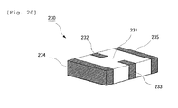
- Fig. 20 is a perspective view showing an external shape of a general filter element.
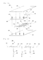
- Fig. 21 is a schematic plan perspective view showing a general multilayered substrate.
- Fig. 22 is a schematic side perspective view showing a general multilayered substrate.
- Fig. 23 is a schematic exploded perspective view showing a general multilayered substrate.
- Fig. 24 is an equivalent circuit of a filter circuit in a general multilayered substrate.
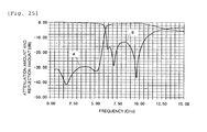
- Fig. 25 is a diagram showing the frequency characteristic of a filter circuit on a general multilayered substrate.
- the resonant circuit based on the general technology which is used in the BPF includes transmission lines 213 and 214 which are connected in series between input and output terminals 211 and 212, a transmission line 215 connected to a junction of the transmission lines 213 and 214 and the ground, and a capacitor 216 connected between the transmission line 215 and the ground.
- a filter circuit 220 which forms a BPF having a pass band of 6 to 10 GHz using the resonant circuit 210, as shown in FIG. 17, includes a capacitor 221 interposed between the input terminal 211 and the input transmission line 213 and a capacitor 222 interposed between the output terminal 212 and the output transmission line 214.
- a frequency characteristic of the filter circuit 220 is as shown in Figs. 18 and 19.
- a curve A is an attenuation characteristic curve
- a curve B is a reflection amount characteristic curve
- a vertical axis represents an attenuation amount and a reflection amount in units of dB
- a horizontal axis represents a frequency in units of GHz.
- the attenuation characteristic curves A in the figures indicate, the attenuation amount has local maximal values at frequencies of 5 GHz, 22.5 GHz, and 43.5 GHz.
- the reflection amount characteristic curves B in the figures indicate, the reflection amount has local minimal values at frequencies of 8.5 GHz and 31.5 GHz.
- FIG. 20 An example of an external shape of a filter element 230 is shown in Fig. 20, when the filter circuit 220 is formed as a circuit element.
- the filter element 230 is formed by stacking the filter circuit 220 inside a layered product 231 having a rectangular parallelepiped shape which is made mainly of dielectric ceramics.
- external terminal electrodes 232 to 235 are formed on a surface of the layered product 231.
- an external terminal electrode 232 corresponds to the input terminal 211
- an external terminal electrode 233 corresponds to the output terminal 212.
- external terminal electrodes 234 and 235 are earth terminals.
- Figs. 21 to 23 The shape and disposition of a conductor pattern are shown in Figs. 21 to 23, when another exemplary BPF to which the filter circuit 220 is applied is formed inside the multilayered substrate.
- a reference numeral 240 denotes a multilayered substrate which is made mainly of dielectric ceramics. Inside the multilayered substrate 240, a filter circuit 290 to be described later is formed by stacking multiple conductor patterns. Described in more details, in the multilayered substrate 240, on both sides of a portion in which the filter circuit 290 is formed, earth conductor patterns 241 and 242 parallel to each other are disposed, respectively. In addition, between the earth conductor patterns 241 and 242, an earth conductor pattern 243 having a predetermined size is formed to be parallel to the earth conductor patterns 241 and 242. The earth conductor pattern 243 is electrically connected to the earth conductor patterns 241 and 242 through a plurality of via conductors 244. In addition, between the earth conductor patterns 241 and 242, an input conductor pattern 250, an output conductor pattern 260, a resonance conductor pattern 270, and a connection conductor pattern 280 are formed.
- the input conductor pattern 250 is formed to be parallel to the earth conductor patterns 241 and 242.
- the input conductor pattern 250 includes an input stripe line 251, a capacitor electrode 252 connected thereto, a stripe line 253 of which one end is connected to the capacitor electrode 252, and a capacitor electrode 254 which is connected to the other end of the stripe line 253.
- the capacitor electrode 254 is disposed to face the earth conductor pattern 243.
- the output conductor pattern 260 is formed to be parallel to the earth conductor patterns 241 and 242 and to be on a same side as the input conductor pattern 250.
- the output conductor pattern 260 includes an output stripe line 261, a capacitor electrode 262 connected thereto, a stripe line 263 of which one end is connected to the capacitor electrode 262 and which is disposed parallel to the stripe line 253, and a capacitor electrode 264 which is connected to the other end of the stripe line 263.
- only the capacitor electrode 264 is disposed to face the earth conductor pattern 243.
- the resonance conductor pattern 270 includes a stripe line 271 which is interposed between the input and output conductor patterns 250 and 260, formed to be on a same side as the input and output conductor patterns 250 and 260, and disposed to be parallel to the stripe line 253 and a capacitor electrode 272 which is connected to one end of the stripe line 271.
- a capacitor electrode 272 which is connected to one end of the stripe line 271.
- only the capacitor electrode 272 is disposed to face the earth conductor pattern 243.
- connection conductor pattern 280 is disposed by disposing dielectric ceramics 240a on a layer different from a layer on which the input conductor pattern 250, the output conductor pattern 260, and the resonance conductor pattern 270 are disposed.
- the connection conductor pattern 280 includes a capacitor electrode 281 which is disposed to face the capacitor electrode 252, a capacitor electrode 285 which is disposed to face the capacitor electrode 262, a stripe line 282 of which one end is connected to the capacitor electrode 281, a connection electrode 283 which is connected to the other end of the stripe line 282, and a stripe line 284 of which one end is connected to the connection electrode 283 and the other end is connected to the capacitor electrode 285.
- the connection electrode 283 is connected to one end of the stripe line 271 through a via conductor 273.
- FIG. 24 An equivalent circuit of a filter circuit which is formed in the multilayered substrate 240 is as shown in Fig. 24.
- components of the equivalent circuit shown in Fig. 24 will now be described.
- a transmission line 293 connected to an input terminal 291 is constructed by the stripe line 251, and a capacitor 221 is constructed by the capacitor electrodes 252 and 281.
- a transmission line 213 is constructed by the stripe line 282.
- a transmission line 294 which is connected to an output terminal 292 is constructed by the stripe line 261, and a capacitor 222 is constructed by the capacitor electrodes 262 and 285.
- a transmission line 214 is constructed by the stripe line 284.
- a series resonant circuit including the transmission line 215 and the capacitor 216 is constructed by the stripe line 271, and the capacitor electrode 272, and the earth conductor pattern 243.
- a series resonant circuit including a transmission line 295 which is connected to a junction of the transmission line 293 and the capacitor 221 and a capacitor 297 is constructed by the stripe line 253, the capacitor electrode 254, and the earth conductor pattern 243.
- a series resonant circuit including a transmission line 296 which is connected to a junction of the transmission line 294 and the capacitor 222 and a capacitor 298 is constructed by the stripe line 263, the capacitor electrode 264, and the earth conductor pattern 243.
- the frequency characteristic of the filter circuit 290 that is a BPF, in the multilayered substrate 240 constructed as described above is as shown in Fig. 25.
- a curve A is an attenuation characteristic curve
- a curve B is a reflection amount characteristic curve
- a vertical axis represents an attenuation amount and a reflection amount in units of dB
- a horizontal axis represents a frequency in units of GHz.
- the attenuation characteristic curve A in the figure indicates, the attenuation amount has local maximal values at frequencies of 1.8 GHz and 5.2 GHz.
- the reflection amount characteristic curve B in the figure indicates, the reflection amount has local minimal values at frequencies of 7.1 GHz and 9.6 GHz.
- the filter circuit 290 is designed on the basis of the filter circuit 220 described above to have a pass band of 6 to 10 GHz.
- the stripe lines 251 and 253 and capacitor electrode 254 which are included in the input conductor pattern 250 shown in Figs. 21 to 23 and the stripe lines 261 and 263 and the capacitor electrode 264 which are included in the output conductor pattern 260 shown in Figs. 21 to 23 can be removed.
- the resonant circuit 210, the filter circuit 220, the filter element 230, and the multilayered substrate 240 which are described above are according to a general embodiment. Accordingly, as a different type of a BPF which can be used in another embodiment, a BPF which is disclosed in JP A-10-126104 is known.
- the band pass filter (BPF) is constructed by using one resonant circuit
- the number of matching frequencies may be increased by using a BPF which is formed by configuring multiple stages of the aforementioned resonant circuit
- the configuration of multiple stages of the resonant circuits results in an increase in a circuit size and insertion loss.
- an attenuation pole does not appear, and accordingly the BPF has a characteristic close to a substantial highpass filter.
- a resonant circuit includes: an input transmission line; an output transmission line of which an input terminal is connected to an output terminal of the input transmission line; a first capacitor of which one terminal is connected to an input terminal of the input transmission line and the other terminal is connected to an output terminal of the output transmission line; a main resonant portion of which one terminal is connected to an output terminal of the input transmission line; a second capacitor of which one terminal serves as an input terminal and the other terminal is connected to the input terminal of the input transmission line; and a third capacitor of which one terminal is connected to the output terminal of the output transmission line and the other terminal serves as an output terminal.
- the number of matching frequencies at which reflection amounts become extreme values is increased by one owing to addition of a first capacitor when compared with a case where the first capacitor is not added to be able to match a broadband, and accordingly low insertion loss can be maintained.
- a multilayered substrate in which an electronic circuit including conductor patterns is buried in a multilayer body includes: an input transmission line portion; an output transmission line portion of which an input terminal is connected to an output terminal of the input transmission line portion; a first capacitor portion of which one terminal is connected to an input terminal of the input transmission line portion and the other terminal is connected to an output terminal of the output transmission line portion; a main resonant portion of which one terminal is connected to an output terminal of the input transmission line portion; a second capacitor portion which is connected to the input terminal of the input transmission line portion; and a third capacitor portion which is connected to the output terminal of the output transmission line portion.
- a BPF is configured by each transmission line portion, the number of matching frequencies at which reflection amounts become extreme values is increased by one owing to addition of a first capacitor when compared with a case where the capacitor is not added to be able to mach a broadband, and accordingly it is possible to maintain low insertion loss.
- an attenuation zone can be formed at a higher cutoff frequency, and accordingly it is possible to implement an excellent attenuation characteristic.
- the number of matching frequencies at which reflection amounts become extreme values is increased by one owing to addition of a first capacitor when compared with a case where the first capacitor is not added, and it is possible to form an attenuation pole in an attenuation zone having high frequencies.
- a BPF is configured, the number of matching frequencies at which reflection amounts become extreme values is increased by one owing to addition of a first capacitor when compared with a case where the first capacitor is not added, and it is possible to match a broadband.
- the filter circuit can represent an excellent attenuation characteristic.
- a BPF is configured by each transmission line portion, the number of matching frequencies at which reflection amounts become extreme values is increased by one owing to addition of a first capacitor when compared with a case where the capacitor is not added, and it is possible to match a broadband.
- the multilayered substrate can represent an excellent attenuation characteristic.
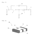
- Fig. 1 is a diagram showing a resonant circuit according to an exemplary embodiment of the present invention.
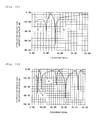
- Figs. 2 and 3 are diagrams showing the frequency characteristics of a resonant circuit according to an exemplary embodiment of the present invention.
- Figs. 4 and 5 are diagrams illustrating an alternative circuit configuration according to another exemplary embodiment of the present invention.
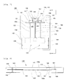
- Fig. 6 is a perspective view showing an external shape of a filter element using a resonant circuit according to an exemplary embodiment of the present invention.
- Fig. 7 is a schematic plan perspective view of a multilayered substrate according to an exemplary embodiment of the present invention.
- Fig. 8 is a schematic side perspective view showing a multilayered substrate according to an exemplary embodiment of the present invention.
- Fig. 1 is a diagram showing a resonant circuit according to an exemplary embodiment of the present invention.
- Figs. 2 and 3 are diagrams showing the frequency characteristics of a resonant circuit according to an exemplary embodiment of the present invention.
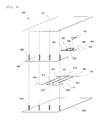
- FIG. 9 is a schematic exploded perspective view showing a multilayered substrate according to an exemplary embodiment of the present invention.
- Fig. 10 is an equivalent circuit of a filter circuit formed on a multilayered substrate according to an exemplary embodiment of the present invention.
- Fig. 11 is a diagram showing the frequency characteristic of a filter circuit formed on a multilayered substrate according to an exemplary embodiment of the present invention.
- a resonant circuit 110 includes input and output transmission lines 113 and 114 which are connected in series between input and output terminals 111 and 112, a main resonant portion including a transmission line 115 of which one end is connected to a junction of the input and output transmission lines 113 and 114 and a capacitor 116 which is connected between the other end of the transmission line 115 and the ground, a capacitor CA connected between an input terminal of the input transmission line 113 and an output terminal of the output transmission line 114, a capacitor 117 interposed between the input terminal 111 and the input terminal of the input transmission line 113, and a capacitor 118 interposed between the output terminal 112 and the output terminal of the output transmission line 114.
- the capacitor 116 is added to one end of the transmission line 115 to shorten a wave length of a signal.
- the resonant circuit 110 includes the input and output transmission lines 113 and 114 as wirings between circuit elements and the capacitor CA connected in parallel thereto.
- the frequency characteristic of the resonant circuit 110 is as shown in Figs. 2 and 3.
- a curve A is an attenuation characteristic curve
- a curve B is a reflection amount characteristic curve
- a vertical axis represents an attenuation amount and a reflection amount in units of dB
- a horizontal axis represents a frequency in units of GHz.
- the attenuation characteristic curves A in the figures indicate, the attenuation amounts have local maximal values at frequencies of 5 GHz, 16.2 GHz, 19.5 GHz, and 40.0 GHz.
- the reflection amount characteristic curves B in the figures indicate, the reflection amounts have local minimal values at frequencies of 8.7 GHz, 11.8 GHz, 25.5 GHz, and 45.0 GHz.
- the capacitor CA By adding the capacitor CA as described above, the number of matching frequencies at which reflection amounts become local minimal values is increased by one from that of a general case, and it is possible to form an attenuation pole in an attenuation zone having high frequencies.
- the capacitor CA since it is possible to match a band broader than a general resonant circuit, low insertion loss can be maintained, and an excellent attenuation characteristic having high frequencies (attenuation zone) can be achieved in the resonant circuit 110.
- a matching frequency and an attenuation pole are added using two input and output transmission lines 113 and 114 which are interposed between the input and output capacitors 117 and 118 and a transmission line 115.
- the addition of an attenuation pole can be achieved with a size of the resonant circuit smaller than that of a case where, as an example, in which an attenuation pole is added by newly forming a parallel resonant circuit.
- This method of adding an attenuation pole makes it possible to reduce an area to be designed and to enhance a characteristic owing to reduction in stray capacitance. As a result, miniaturization of the resonant circuit and an electrical characteristic appropriate for broadband application can be achieved.
- a circuit using an open-terminated transmission line LX1 as shown in Fig. 4 or an short-terminated transmission line LX2 as shown in Fig. 5 may be considered instead of using a combination of the transmission line 115 and the capacitor 116.
- the filter element 130 is formed by stacking the resonant circuit 110 inside a layered product 131 having a rectangular parallelepiped shape which is made mainly of dielectric ceramics.
- external terminal electrodes 132 to 135 are formed on a surface of the layered product 131.
- an external terminal electrode 132 corresponds to the input terminal 111
- an external terminal electrode 133 corresponds to the output terminal 112.
- external terminal electrodes 134 and 135 are earth terminals.
- Figs. 7 to 9 The shape and disposition of a conductor pattern are shown in Figs. 7 to 9, when another exemplary BPF to which the resonant circuit 110 is applied is formed inside the multilayered substrate.
- a reference numeral 140 denotes a multilayered substrate, and the multilayered substrate 140 is made mainly of dielectric ceramics 140a.
- a filter circuit 190 to be described later is formed by stacking multiple conductor patterns inside the multilayered substrate 240. Described in more details, in the multilayered substrate 140, on both sides of a portion in which the filter circuit 190 is formed, earth conductor patterns 141 and 142 parallel to each other are disposed, respectively. In addition, between the earth conductor patterns 141 and 142, an earth conductor pattern 143 having a predetermined size is formed to be parallel to the earth conductor patterns 141 and 142.
- the earth conductor pattern 143 is electrically connected to the earth conductor patterns 141 and 142 through a plurality of via conductors 144. In addition, between the earth conductor patterns 141 and 142, an input conductor pattern 150, an output conductor pattern 160, a resonance conductor pattern 170, and a connection conductor pattern 180 are formed.
- the input conductor pattern 150 is formed to be parallel to the earth conductor patterns 141 and 142.
- the input conductor pattern 150 includes a second main resonant portion including an input stripe line 151, a capacitor electrode 152 of a second capacitor portion connected thereto, a stripe line 153 of which one end is connected to the capacitor electrode 152, and a capacitor electrode 154 which is connected to the other end of the stripe line 153.
- the capacitor electrode 154 is disposed to face the earth conductor pattern 143.
- the output conductor pattern 160 is formed to be parallel to the earth conductor patterns 141 and 142 and to be on a same side as the input conductor pattern 150.
- the output conductor pattern 160 includes a third main resonant portion including an output stripe line 161, a capacitor electrode 162 of a third capacitor portion connected thereto, a stripe line 163 of which one end is connected to the capacitor electrode 162 and which is disposed parallel to the stripe line 153, and a capacitor electrode 164 which is connected to the other end of the stripe line 163.
- only the capacitor electrode 164 is disposed to face the earth conductor pattern 143.
- the resonance conductor pattern 170 includes a first main resonant portion including a stripe line 171 which is interposed between the input and output conductor patterns 150 and 160, formed to be on a same side as the input and output conductor patterns 150 and 160, and disposed to be parallel to the stripe line 153 and a capacitor electrode 172 which is connected to one end of the stripe line 171.
- a capacitor electrode 172 which is disposed to face the earth conductor pattern 143.
- the connection conductor pattern 180 is disposed by disposing dielectric ceramics 140a on a layer different from a layer on which the input conductor pattern 150, the output conductor pattern 160, and the resonance conductor pattern 170 are disposed.
- the connection conductor pattern 180 includes a conduction pattern forming a capacitor electrode 181 of the second capacitor portion which is disposed to face the capacitor electrode 152, a capacitor electrode 185 of the third capacitor portion which is disposed to face the capacitor electrode 162, a stripe line 182 of which one end is connected to the capacitor electrode 181, a connection electrode 183 which is connected to the other end of the stripe line 182, a stripe line 184 of which one end is connected to the connection electrode 183 and the other end is connected to the capacitor electrode 185, and a capacitor electrode 186 of the first capacitor portion which is connected to the capacitor electrode 181 of the first capacitor portion into one body and a capacitor electrode 187 of the first capacitor portion of which an open end portion is disposed to face an open end portion of the capacitor electrode 186 by interposing the
- FIG. 10 An equivalent circuit of a filter circuit which is formed inside the multilayered substrate 140 is as shown in Fig. 10.
- circuit components of the equivalent circuit shown in Fig. 10 are as below.
- a transmission line 193 connected to an input terminal 191 is constructed by the stripe line 153, and a capacitor 121 is constructed by the capacitor electrodes 152 and 181.
- a transmission line 113 is constructed by the stripe line 182.
- a transmission line 194 which is connected to an output terminal 192 is constructed by the stripe line 163, and a capacitor 122 is constructed by the capacitor electrodes 162 and 185.
- a transmission line 114 is constructed by the stripe line 184.
- a main resonant circuit including the transmission line 115 and the capacitor 116 is constructed by the stripe line 171, and the capacitor electrode 172, and the earth conductor pattern 143.
- the capacitor CA connected between then input terminal of the input transmission line 113 and the output terminal of the output transmission line 114 includes the capacitor electrode 186 and the capacitor electrode 187 which is disposed to face the capacitor electrode 186.
- a serial resonant circuit including the transmission line 193 which is connected to the input terminal 191 and the capacitor 195 includes the stripe line 153, the capacitor electrode 154, and the earth conductor pattern 143.
- a series resonant circuit including the transmission line 194 which is connected to the output terminal 192 and the capacitor 196 includes the stripe line 163, the capacitor electrode 164, and the earth conductor pattern 143.
- the frequency characteristic of the filter circuit 190 that is a band-pass filter, having the aforementioned structure, in the multilayered substrate 140 is as shown in Fig. 11.
- a curve A is an attenuation characteristic curve
- a curve B is a reflection amount characteristic curve
- a vertical axis represents an attenuation amount and a reflection amount in units of dB
- a horizontal axis represents a frequency in units of GHz.
- the attenuation amounts have local maximal values at frequencies of 1.8 GHz, 5.2 GHz, and 11.3 GHz.
- the reflection amounts have local minimal values at frequencies of 6.5 GHz, 7.0 GHz, 8.8 GHz, and 10.5 GHz.
- the filter circuit 190 is designed on the basis of the filter circuit 110 described above to have a pass band of 6 to 10 GHz.
- the filter circuit 190 described above is completed by connecting in series three resonant circuits which are implemented in a ceramic multilayered substrate as three stages through a combination of the resonant circuit 110 according to the embodiment of the invention and the general resonant circuit.
- the BPF 190 having three stages according to the embodiment of the invention has four matching frequencies and an additional attenuation pole at a high frequency (attenuation zone).
- the general resonant circuit 290 has three matching frequencies and cannot have an additional attenuation pole in an attenuation zone having high frequencies. It is apparent that the BPF 190 using the resonant circuit 110 according to the embodiment of the invention has advantages in broadband and high attenuation characteristics when the electrical characteristics of the BPF 190 according to the embodiment of the invention and the general BPF 190 are compared.
- the stripe lines 151 and 153 and capacitor electrode 154 which are included in the input conductor pattern 150 shown in Figs. 7 to 9 and the stripe lines 161 and 163 and the capacitor electrode 164 which are included in the output conductor pattern 160 shown in Figs. 7 to 9 can be removed.
- a BPF may be configured by connecting the two or more resonant circuits 110 shown in Fig. 1 in series.
- a BPF 300 in Fig. 12 is configured by connecting two resonant circuits 110 between an input terminal 301 and an output terminal 302.
- a capacitor 312 is common to one resonant circuit serving as the second capacitor (input capacitor) and to the other resonant circuit serving the third capacitor (output capacitor).
- the frequency characteristic of the BPF 300 is as shown in Fig. 13.
- a curve A is an attenuation characteristic curve
- a curve B is a reflection amount characteristic curve
- a vertical axis represents an attenuation amount and a reflection amount in units of dB
- a horizontal axis represents a frequency in units of GHz.
- the attenuation amount have local maximal values at frequencies of 4.8 GHz and 17.5 GHz.
- the reflection amount characteristic curve B in the figure indicates, the reflection amounts have local minimal values at frequencies of 6.7 GHz, 8.6 GHz, 12.0 GHz, and 14.3 GHz.
- the filter circuit 300 is designed to have a pass band of 6 to 10 GHz.
- a BPF 400 in Fig. 14 is configured by connecting three resonant circuits 110 in series between an input terminal 401 and an output terminal 402.
- the frequency characteristic of the BPF 400 is as shown in Fig. 15.
- a curve A is an attenuation characteristic curve
- a curve B is a reflection amount characteristic curve
- a vertical axis represents an attenuation amount and a reflection amount in units of dB
- a horizontal axis represents a frequency in units of GHz.
- the attenuation amount have local maximal values at frequencies of 4.5 GHz, 5. 0 GHz, 16.5 GHz, and 20.0 GHz.
- the reflection amounts have local minimal values at frequencies of 6.3 GHz, 7.0 GHz, 9.0 GHz, 11.8 GHz, 13.8 GHz, and 14.8 GHz.
- the filter circuit 400 is designed to have a pass band of 6 to 15 GHz.
- a BPF having superior frequency characteristics can be configured.
Landscapes
- Engineering & Computer Science (AREA)
- Power Engineering (AREA)
- Manufacturing & Machinery (AREA)
- Microelectronics & Electronic Packaging (AREA)
- Physics & Mathematics (AREA)
- Electromagnetism (AREA)
- Filters And Equalizers (AREA)
- Control Of Motors That Do Not Use Commutators (AREA)
Applications Claiming Priority (1)
| Application Number | Priority Date | Filing Date | Title |
|---|---|---|---|
| JP2005375484A JP5016219B2 (ja) | 2005-12-27 | 2005-12-27 | 共振回路、フィルタ回路、及び多層基板 |
Publications (2)
| Publication Number | Publication Date |
|---|---|
| EP1806841A2 true EP1806841A2 (fr) | 2007-07-11 |
| EP1806841A3 EP1806841A3 (fr) | 2008-02-27 |
Family
ID=37907123
Family Applications (1)
| Application Number | Title | Priority Date | Filing Date |
|---|---|---|---|
| EP06256360A Withdrawn EP1806841A3 (fr) | 2005-12-27 | 2006-12-14 | Circuit de résonance, circuit de filtre, et substrat multicouches |
Country Status (3)
| Country | Link |
|---|---|
| US (1) | US7782157B2 (fr) |
| EP (1) | EP1806841A3 (fr) |
| JP (1) | JP5016219B2 (fr) |
Families Citing this family (5)
| Publication number | Priority date | Publication date | Assignee | Title |
|---|---|---|---|---|
| US20090027141A1 (en) * | 2007-06-22 | 2009-01-29 | Taiyo Yuden Co., Ltd. | Filter circuit, filter circuit device, multilayered circuit board, and circuit module each including the filter circuit |
| US8680952B2 (en) * | 2008-12-30 | 2014-03-25 | Tdk Corporation | Bandpass filter with dual band response |
| JPWO2010113845A1 (ja) * | 2009-04-03 | 2012-10-11 | 太陽誘電株式会社 | 分布定数回路 |
| TWI656732B (zh) * | 2017-10-16 | 2019-04-11 | 國立臺灣大學 | 可調式濾波器 |
| WO2026058570A1 (fr) * | 2024-09-11 | 2026-03-19 | 株式会社村田製作所 | Filtre haute fréquence, et filtre de bruit de mode commun |
Citations (2)
| Publication number | Priority date | Publication date | Assignee | Title |
|---|---|---|---|---|
| JPS58190113A (ja) | 1982-04-30 | 1983-11-07 | Fujitsu Ltd | 遅延等化器 |
| JPS5913403B2 (ja) | 1979-12-13 | 1984-03-29 | 大同特殊鋼株式会社 | 被処理物の搬送方法 |
Family Cites Families (12)
| Publication number | Priority date | Publication date | Assignee | Title |
|---|---|---|---|---|
| GB813962A (en) * | 1957-05-22 | 1959-05-27 | Standard Telephones Cables Ltd | Improvements in or relating to electric wave filters |
| JPS5679502A (en) * | 1979-11-30 | 1981-06-30 | Matsushita Electric Ind Co Ltd | Band block filter and antenna duplexer |
| JPS5913403A (ja) * | 1982-07-15 | 1984-01-24 | Alps Electric Co Ltd | トラツプを有する帯域通過フイルタ |
| JPH04225601A (ja) * | 1990-12-27 | 1992-08-14 | Sharp Corp | 帯域除去フィルタ回路 |
| JP3381956B2 (ja) * | 1993-03-01 | 2003-03-04 | 日本碍子株式会社 | 積層型誘電体フィルタ |
| JPH10126104A (ja) * | 1996-10-22 | 1998-05-15 | Kyocera Corp | 積層型誘電体フィルタ |
| US6711394B2 (en) * | 1998-08-06 | 2004-03-23 | Isco International, Inc. | RF receiver having cascaded filters and an intermediate amplifier stage |
| JP2957573B1 (ja) * | 1998-09-04 | 1999-10-04 | ティーディーケイ株式会社 | 積層型フィルタ |
| US6300849B1 (en) * | 1998-11-27 | 2001-10-09 | Kyocera Corporation | Distributed element filter |
| US6621370B1 (en) * | 2000-09-15 | 2003-09-16 | Atheros Communications, Inc. | Method and system for a lumped-distributed balun |
| US7099645B2 (en) * | 2001-12-25 | 2006-08-29 | Ngk Spark Plug Co., Ltd. | Multilayer LC filter |
| KR100616674B1 (ko) * | 2005-02-16 | 2006-08-28 | 삼성전기주식회사 | 저지대역 감쇄특성을 개선한 적층형 필터 |
-
2005
- 2005-12-27 JP JP2005375484A patent/JP5016219B2/ja not_active Expired - Fee Related
-
2006
- 2006-12-14 EP EP06256360A patent/EP1806841A3/fr not_active Withdrawn
- 2006-12-20 US US11/642,415 patent/US7782157B2/en not_active Expired - Fee Related
Patent Citations (2)
| Publication number | Priority date | Publication date | Assignee | Title |
|---|---|---|---|---|
| JPS5913403B2 (ja) | 1979-12-13 | 1984-03-29 | 大同特殊鋼株式会社 | 被処理物の搬送方法 |
| JPS58190113A (ja) | 1982-04-30 | 1983-11-07 | Fujitsu Ltd | 遅延等化器 |
Also Published As
| Publication number | Publication date |
|---|---|
| EP1806841A3 (fr) | 2008-02-27 |
| JP2007180781A (ja) | 2007-07-12 |
| JP5016219B2 (ja) | 2012-09-05 |
| US20070188273A1 (en) | 2007-08-16 |
| US7782157B2 (en) | 2010-08-24 |
Similar Documents
| Publication | Publication Date | Title |
|---|---|---|
| US9077061B2 (en) | Directional coupler | |
| US6380608B1 (en) | Multiple level spiral inductors used to form a filter in a printed circuit board | |
| CN104937845B (zh) | 复合lc谐振器及带通滤波器 | |
| US8536956B2 (en) | Directional coupler | |
| US8283990B2 (en) | Signal transmission communication unit and coupler | |
| KR20110042171A (ko) | 밴드 패스 필터, 고주파 부품 및 통신 장치 | |
| US7183872B2 (en) | Laminated balun transformer | |
| JP5804076B2 (ja) | Lcフィルタ回路及び高周波モジュール | |
| US7671704B2 (en) | LC resonant circuit | |
| JP2004312065A (ja) | 受動部品 | |
| US7336144B2 (en) | Compact multilayer band-pass filter and method using interdigital capacitor | |
| JP4539422B2 (ja) | チップ型多段フィルタ装置 | |
| WO2015059963A1 (fr) | Résonateur lc composite et filtre passe-bande | |
| US7782157B2 (en) | Resonant circuit, filter circuit, and multilayered substrate | |
| US20230318560A1 (en) | Band-pass filter | |
| US8400236B2 (en) | Electronic component | |
| JP2010183513A (ja) | 積層型バンドパスフィルタおよび高周波モジュール | |
| JP4245265B2 (ja) | 複数のフィルタを有する多層配線基板 | |
| JPH1197962A (ja) | 高周波部品 | |
| HK1106076A (en) | Resonant circuit, filter circuit, and multilayered substrate | |
| JP4339819B2 (ja) | ハイパスフィルタ | |
| US20250233578A1 (en) | Filter circuit | |
| CN214672907U (zh) | 一种带通滤波器 | |
| EP1816701A1 (fr) | Pièce passive | |
| JP2002374102A (ja) | 積層型誘電体フィルタ |
Legal Events
| Date | Code | Title | Description |
|---|---|---|---|
| PUAI | Public reference made under article 153(3) epc to a published international application that has entered the european phase |
Free format text: ORIGINAL CODE: 0009012 |
|
| AK | Designated contracting states |
Kind code of ref document: A2 Designated state(s): AT BE BG CH CY CZ DE DK EE ES FI FR GB GR HU IE IS IT LI LT LU LV MC NL PL PT RO SE SI SK TR |
|
| AX | Request for extension of the european patent |
Extension state: AL BA HR MK YU |
|
| PUAL | Search report despatched |
Free format text: ORIGINAL CODE: 0009013 |
|
| 17P | Request for examination filed |
Effective date: 20071218 |
|
| AK | Designated contracting states |
Kind code of ref document: A3 Designated state(s): AT BE BG CH CY CZ DE DK EE ES FI FR GB GR HU IE IS IT LI LT LU LV MC NL PL PT RO SE SI SK TR |
|
| AX | Request for extension of the european patent |
Extension state: AL BA HR MK YU |
|
| REG | Reference to a national code |
Ref country code: HK Ref legal event code: DE Ref document number: 1106076 Country of ref document: HK |
|
| 17Q | First examination report despatched |
Effective date: 20080922 |
|
| AKX | Designation fees paid |
Designated state(s): AT BE BG CH CY CZ DE DK EE ES FI FR GB GR HU IE IS IT LI LT LU LV MC NL PL PT RO SE SI SK TR |
|
| APBK | Appeal reference recorded |
Free format text: ORIGINAL CODE: EPIDOSNREFNE |
|
| APBN | Date of receipt of notice of appeal recorded |
Free format text: ORIGINAL CODE: EPIDOSNNOA2E |
|
| APBR | Date of receipt of statement of grounds of appeal recorded |
Free format text: ORIGINAL CODE: EPIDOSNNOA3E |
|
| APAF | Appeal reference modified |
Free format text: ORIGINAL CODE: EPIDOSCREFNE |
|
| REG | Reference to a national code |
Ref country code: HK Ref legal event code: WD Ref document number: 1106076 Country of ref document: HK |
|
| APBT | Appeal procedure closed |
Free format text: ORIGINAL CODE: EPIDOSNNOA9E |
|
| STAA | Information on the status of an ep patent application or granted ep patent |
Free format text: STATUS: THE APPLICATION IS DEEMED TO BE WITHDRAWN |
|
| 18D | Application deemed to be withdrawn |
Effective date: 20140701 |