EP1808716A1 - Plattenförmiger Lichtleiter und Anzeigevorrichtung mit dem Lichtleiter - Google Patents
Plattenförmiger Lichtleiter und Anzeigevorrichtung mit dem Lichtleiter Download PDFInfo
- Publication number
- EP1808716A1 EP1808716A1 EP20060254308 EP06254308A EP1808716A1 EP 1808716 A1 EP1808716 A1 EP 1808716A1 EP 20060254308 EP20060254308 EP 20060254308 EP 06254308 A EP06254308 A EP 06254308A EP 1808716 A1 EP1808716 A1 EP 1808716A1
- Authority
- EP
- European Patent Office
- Prior art keywords
- light
- guide panel
- light guide
- dark portion
- incidence
- Prior art date
- Legal status (The legal status is an assumption and is not a legal conclusion. Google has not performed a legal analysis and makes no representation as to the accuracy of the status listed.)
- Granted
Links
Images


Classifications
-
- G—PHYSICS
- G02—OPTICS
- G02B—OPTICAL ELEMENTS, SYSTEMS OR APPARATUS
- G02B6/00—Light guides; Structural details of arrangements comprising light guides and other optical elements, e.g. couplings
- G02B6/0001—Light guides; Structural details of arrangements comprising light guides and other optical elements, e.g. couplings specially adapted for lighting devices or systems
- G02B6/0011—Light guides; Structural details of arrangements comprising light guides and other optical elements, e.g. couplings specially adapted for lighting devices or systems the light guides being planar or of plate-like form
-
- F—MECHANICAL ENGINEERING; LIGHTING; HEATING; WEAPONS; BLASTING
- F24—HEATING; RANGES; VENTILATING
- F24F—AIR-CONDITIONING; AIR-HUMIDIFICATION; VENTILATION; USE OF AIR CURRENTS FOR SCREENING
- F24F6/00—Air-humidification, e.g. cooling by humidification
- F24F6/12—Air-humidification, e.g. cooling by humidification by forming water dispersions in the air
- F24F6/14—Air-humidification, e.g. cooling by humidification by forming water dispersions in the air using nozzles
-
- G—PHYSICS
- G02—OPTICS
- G02B—OPTICAL ELEMENTS, SYSTEMS OR APPARATUS
- G02B6/00—Light guides; Structural details of arrangements comprising light guides and other optical elements, e.g. couplings
- G02B6/0001—Light guides; Structural details of arrangements comprising light guides and other optical elements, e.g. couplings specially adapted for lighting devices or systems
- G02B6/0011—Light guides; Structural details of arrangements comprising light guides and other optical elements, e.g. couplings specially adapted for lighting devices or systems the light guides being planar or of plate-like form
- G02B6/0013—Means for improving the coupling-in of light from the light source into the light guide
- G02B6/0015—Means for improving the coupling-in of light from the light source into the light guide provided on the surface of the light guide or in the bulk of it
- G02B6/0016—Grooves, prisms, gratings, scattering particles or rough surfaces
-
- G—PHYSICS
- G02—OPTICS
- G02B—OPTICAL ELEMENTS, SYSTEMS OR APPARATUS
- G02B6/00—Light guides; Structural details of arrangements comprising light guides and other optical elements, e.g. couplings
- G02B6/0001—Light guides; Structural details of arrangements comprising light guides and other optical elements, e.g. couplings specially adapted for lighting devices or systems
- G02B6/0011—Light guides; Structural details of arrangements comprising light guides and other optical elements, e.g. couplings specially adapted for lighting devices or systems the light guides being planar or of plate-like form
- G02B6/0013—Means for improving the coupling-in of light from the light source into the light guide
- G02B6/0015—Means for improving the coupling-in of light from the light source into the light guide provided on the surface of the light guide or in the bulk of it
- G02B6/0018—Redirecting means on the surface of the light guide
-
- Y—GENERAL TAGGING OF NEW TECHNOLOGICAL DEVELOPMENTS; GENERAL TAGGING OF CROSS-SECTIONAL TECHNOLOGIES SPANNING OVER SEVERAL SECTIONS OF THE IPC; TECHNICAL SUBJECTS COVERED BY FORMER USPC CROSS-REFERENCE ART COLLECTIONS [XRACs] AND DIGESTS
- Y10—TECHNICAL SUBJECTS COVERED BY FORMER USPC
- Y10S—TECHNICAL SUBJECTS COVERED BY FORMER USPC CROSS-REFERENCE ART COLLECTIONS [XRACs] AND DIGESTS
- Y10S385/00—Optical waveguides
- Y10S385/901—Illuminating or display apparatus
Definitions
- the present invention relates to a light guide panel in which the generation of dark portions in a light incidence area is reduced and a display device employing the same.
- liquid crystal displays which are light receiving type flat displays used in laptop computers, desktop computers, LCD TVs, and mobile communication terminals, do not form images by emitting light by themselves but by selectively emitting illumination light radiated from an external source such as backlight units installed behind the liquid crystal displays.
- Backlight units can be classified into direct light type backlight units and edge light type backlight units according to the arrangement of a light source.
- a direct light type backlight unit includes a plurality of lamps that are installed directly under a liquid crystal display and emit light directly onto a liquid crystal panel.
- a light source of the direct light type backlight unit can be installed in a desired position on a broad surface, and thus is appropriate for a large screen display device such as an LCD TV larger than 30 inches.
- An edge light type backlight unit is appropriate for small or medium sized displays like monitors or cell phones since the light source thereof is installed at a lateral side of a light guide panel.
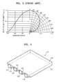
- FIG. 1 is a perspective view of a conventional edge light type backlight unit.
- a light emitting device (LED) 10 installed at a side of a light guide panel (LGP) 20 emits light, and the emitted light is transferred to a liquid crystal panel via the LGP 20.
- a lower surface 15 of the LGP 20 is a reflection surface for advancing light toward the display panel. The light emitted from the LED 10 is converted into surface light by the LGP 20 and exit through an upper surface 17 of the LGP 20.
- FIG. 2 illustrates the light from the LED 10 traveling through the LGP 20.
- dark portions D having low brightness are created on the incident surface of the LGP 20 because of relatively little light arriving from the light source.
- FIG. 3 illustrates light emitting efficiency according to the light emission angle of the LED 10. The light emitting efficiency of the LED 10 decreases from 0 ° to 90°. In other words, most of the light from the LED 10 is emitted forward, and thus the amount of light emitted laterally is relatively small. Accordingly, as illustrated in FIG. 2, the dark portions D, that is, areas where small quantities of light arrive from the LED 10, exist. The dark portions D cause irregular brightness and thus result in decreased display quality.
- an area within a distance d from the LED 10, where the dark portions D are created, is not included in a screen. That is, the area not including the dark portions D is used as an effective screen 25.
- the area within the distance d from the LED 10 is unused, and thus the miniaturization of the backlight unit is difficult.
- the present invention provides a light guide panel in which the generation of dark portions where little light exists is reduced to provide uniform brightness and a display device employing the light guide panel.
- a light guide panel comprising: an incidence surface facing a plurality of light sources separated apart a predetermined distance; at least one dark portion reducing unit that is formed on the incidence surface between adjacent pairs of the light sources and at both edges of the incidence surface, and reflects the light incident from the light sources to reduce the creation of dark portion; an upper surface transmitting a portion of incident light and reflecting the rest of the incident light; and a lower surface facing the upper surface and reflecting the light incident from the incidence surfaces and dark portion reducing units.
- the dark portion reducing units may be grooves that are oblique from the incidence surfaces toward the lower surface.
- the dark portion reducing units may be formed into curved surface or have a plurality of flat surfaces.
- the dark portion reducing units may be semi-conical or semispherical.
- the dark portion reducing units may be semi-pyramidal.
- the dark portion reducing units may be symmetrical about vertical center lines.
- a vertex on the incidence surfaces of the dark portion reducing units may be separated from the upper surface.
- Diffusion units that are disposed on the incidence surface facing the light sources and diffuse the incident light from the light sources may be further included.
- Each of the diffusion units may have a saw-toothed pattern.
- a display device comprising: a plurality of light sources; a light guide panel comprising: an incidence surface facing the light sources; at least one dark portion reducing unit that is formed on the incidence surface between adjacent pairs of the light sources and at both edges of the incidence surface, and reflects the light incident from the light sources to reduce the creation of dark portion; an upper surface transmitting a portion of incident light and reflecting the rest of the incident light; and a lower surface facing the upper surface and reflecting the light incident from the incidence surfaces and dark portion reducing units; and a display panel forming an image using the light from the light guide panel.
- FIG. 4 is a perspective view of a light guide panel 110 according to an embodiment of the present invention.
- the light guide panel 110 includes an incidence surface 102 facing a plurality of light sources 100 that are separated a predetermined distance, and dark portion reducing units 105.
- the light guide panel 110 guides the light received from the light sources 100 formed at a lateral side of the light guide panel 110 to a screen (not shown) and includes an upper surface 109 transmitting a portion of incident light toward the screen and reflecting the rest of the light and a lower surface 107 facing the upper surface 109 and reflecting incident light.
- the dark portion reducing units 105 reduce the creation of the dark portions where relatively less light arrives from the light sources 100 and are formed of grooves that are oblique and extend between incidence surfaces 102 and the lower surface 107.
- the dark portion reducing units 105 may be curved in shape of, for example, semi-cones or hemispheres.
- the dark portion reducing units 105 are symmetrical about vertical center lines C as illustrated in FIG. 5, and a vertex 106 exists on the vertical center line C. Since the dark portion reducing portions 105 are symmetrical, light from the light sources 100 is reflected symmetrically, and thus can improve the uniformity of the brightness. Also, the vertex 106 is disposed a predetermined distance from the upper surface 109, and thus a reduction in an effective surface of the upper surface 109 due to the dark portion reducing units 105 is prevented.
- the light sources 100 may be, for example, light emitting diodes and emit light through a light emitting window 101.
- the light emitted from the light sources 100 passes through the incidence surfaces 102 and travels forward or sideward. A portion of the light travelling sideways is reflected by the dark portion reducing units 105 and proceeds toward the upper surface 109.
- the light proceeding upward is transmitted through the upper surface 109 or is reflected to the lower surface 107.
- a portion of the light proceeding sideways from the light sources 100 proceeds via the dark portion reducing units 105 toward the upper surface 109, and thus light is supplied to the region above the dark portion reducing units 105.
- the creation of dark portions can be suppressed.
- the dark portion reducing units 105 are disposed in an area where relatively less light arrives, that is, on incidence surfaces between the light sources 100 and at both edges of the incidence surfaces 102. At least one dark portion reducing unit 105 is formed between each pair of the adjacent light sources 100, and a plurality of dark portion reducing units 105 may be formed as illustrated in FIG. 6.
- dark portion reducing units 105' may have flat sides as illustrated in FIG. 7A, for example, in the form of semi-pyramids.
- the shape of the dark portion reducing units 105' is shown as a semi-pyramid in FIG. 7A, but the shape may be any polygon having more than three triangular surfaces.
- Each of the dark portion reducing units 105' has a vertex 106' disposed a predetermined distance away from the upper surface 109.
- FIG. 7B a portion of the light emitted from the light emitting window 101 of the light source 100 proceeds to the upper surface 109 and the other portion of the light proceeds sideways.
- a portion of the light proceeding sideways is reflected by the dark portion reducing units 105' and heads to the upper surface 109.
- a portion of the light is transmitted through the upper surface 109, and the rest of the light is reflected toward the lower surface 107.
- the upper surface 109 has a critical angle depending on the difference between the refractive index of the light guide panel 100 and the refractive index of the medium outside of the light guide panel 100. The light incident at an angle smaller than the critical angle is transmitted and the light incident at an angle greater than the critical angle is reflected.
- the dark portion reducing units 105' are formed on the incidence surfaces between the light sources 100 and at both edges of the incidence surface 102.
- the light guide panel 110 may further include diffusion units 120 that are disposed in positions corresponding to the light sources 100 and diffuse the incident light onto incidence surfaces 102 facing the light sources 100.
- the diffusion units 120 diffuse the light received from the light sources 100 sideward to regulate brightness. That is, the light from the light sources 100 is refracted and reflected through the diffusion unit 120 forward and sideward, and a portion of the light proceeding sideward is reflected toward the upper surface by the dark portion reducing units 105 or 105', thereby suppressing the creation of the dark portions.
- the light transmitting through the incidence surfaces 102 is reflected by the lower surface 107 and the upper surface 109 and proceeds to a surface 112 opposite to the incidence surfaces 102. A portion of the light proceeding from the incidence surfaces 102 to the surface 112 is transmitted through the upper surface 109 and proceeds toward a display panel (170 in FIG. 10), which will be described later.
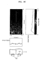
- FIG. 9A illustrates the brightness of light on an incidence surface of a conventional light guide panel in an x-direction and in a light guide panel in a z-direction (the direction from the incidence surface to a surface opposite to the incidence surface) while light is radiated to the light guide panel (LGP) by a conventional LED.
- FIG. 9B illustrates the brightness of light on an incidence surface of a conventional light guide panel in the x-direction and the z-direction when the light guide panel includes only a diffusion unit 120. Though the diffusion unit 120 is formed, there are portions where the brightness between the LEDs is relatively low.
- FIG. 9C illustrates the brightness on the incidence surface of a light guide panel according to an embodiment of the present invention in the x-direction and in a light guide panel in the z-direction when the dark portion reducing units 105 are formed on the incidence surface between the LEDs 100 and diffusion units 120 facing the LEDs 100 are formed.
- the brightness is uniform in the x-direction, and the dark portion is reduced.
- FIG. 10 is a cross-sectional view of a display device according to an embodiment of the present invention.
- the display device includes a backlight unit 150 and a display panel 170 forming an image with the light radiated from the backlight unit 150.
- the backlight unit 150 includes a light source 100 and a light guide panel 110 guiding the light radiated from the light source 100 toward the display panel 170.
- a diffusion plate 153 diffusing light and first and second prism sheets 155 and 157 correcting the light path are disposed between the light guide panel 110 and the display panel 170.
- the first and second prism sheets 155 and 157 cross each other and refract and focus the light from the diffusion plate 153 to improve the directivity of the light, thereby increasing the brightness and reducing the incidence angle of the light.
- the display panel 170 may be a liquid crystal panel.
- a polarization enhancement film 160 may be further included above the second prism sheet 157, that is, the brightness enhancement film.
- the polarization enhancement film 160 may, for example, transmit p-polarized light and reflect s-polarized light, and thus transmit most of the incident light as p-polarized light.
- the light sources 100 are formed on one side of the light guide panel 110. However, the light sources 100 may also be formed on both sides in order to provide more light. When the light sources 100 are formed on both sides, dark portion reducing units are formed on each incidence surface of the light guide panel 110.
- the light guide panel according to the present invention includes dark portion reducing units to reduce the distance between the light source and the light guide panel, thereby reducing a useless surface of a screen caused by dark portions.
- the display device including the light guide panel can be simplified and effectively applied to cell phones or small-sized terminals.
Landscapes
- Physics & Mathematics (AREA)
- General Physics & Mathematics (AREA)
- Optics & Photonics (AREA)
- Chemical & Material Sciences (AREA)
- Engineering & Computer Science (AREA)
- Dispersion Chemistry (AREA)
- Combustion & Propulsion (AREA)
- Mechanical Engineering (AREA)
- General Engineering & Computer Science (AREA)
- Planar Illumination Modules (AREA)
- Liquid Crystal (AREA)
Priority Applications (1)
| Application Number | Priority Date | Filing Date | Title |
|---|---|---|---|
| EP20100186058 EP2293124B1 (de) | 2006-01-16 | 2006-08-16 | Plattenförmiger Lichtleiter und Anzeigevorrichtung mit dem Lichtleiter |
Applications Claiming Priority (1)
| Application Number | Priority Date | Filing Date | Title |
|---|---|---|---|
| KR1020060004479A KR100790857B1 (ko) | 2006-01-16 | 2006-01-16 | 도광판 및 이를 채용한 디스플레이 장치 |
Related Child Applications (2)
| Application Number | Title | Priority Date | Filing Date |
|---|---|---|---|
| EP20100186058 Division EP2293124B1 (de) | 2006-01-16 | 2006-08-16 | Plattenförmiger Lichtleiter und Anzeigevorrichtung mit dem Lichtleiter |
| EP10186058.3 Division-Into | 2010-10-01 |
Publications (2)
| Publication Number | Publication Date |
|---|---|
| EP1808716A1 true EP1808716A1 (de) | 2007-07-18 |
| EP1808716B1 EP1808716B1 (de) | 2012-04-18 |
Family
ID=37807912
Family Applications (2)
| Application Number | Title | Priority Date | Filing Date |
|---|---|---|---|
| EP20100186058 Active EP2293124B1 (de) | 2006-01-16 | 2006-08-16 | Plattenförmiger Lichtleiter und Anzeigevorrichtung mit dem Lichtleiter |
| EP20060254308 Active EP1808716B1 (de) | 2006-01-16 | 2006-08-16 | Plattenförmiger Lichtleiter und Anzeigevorrichtung mit dem Lichtleiter |
Family Applications Before (1)
| Application Number | Title | Priority Date | Filing Date |
|---|---|---|---|
| EP20100186058 Active EP2293124B1 (de) | 2006-01-16 | 2006-08-16 | Plattenförmiger Lichtleiter und Anzeigevorrichtung mit dem Lichtleiter |
Country Status (5)
| Country | Link |
|---|---|
| US (1) | US7573543B2 (de) |
| EP (2) | EP2293124B1 (de) |
| JP (1) | JP5130434B2 (de) |
| KR (1) | KR100790857B1 (de) |
| CN (1) | CN101004253B (de) |
Cited By (1)
| Publication number | Priority date | Publication date | Assignee | Title |
|---|---|---|---|---|
| EP3502543A1 (de) * | 2017-12-20 | 2019-06-26 | ITZ Innovations- und Technologiezentrum GmbH | Flächiges oder stabförmiges lichtleiterelement |
Families Citing this family (15)
| Publication number | Priority date | Publication date | Assignee | Title |
|---|---|---|---|---|
| CN101196597A (zh) * | 2006-12-08 | 2008-06-11 | 鸿富锦精密工业(深圳)有限公司 | 导光板及背光模组 |
| TW200933247A (en) * | 2008-01-24 | 2009-08-01 | Nano Prec Corp | Side-type backlight module |
| TW201035641A (en) * | 2009-03-19 | 2010-10-01 | Advanced Optoelectronic Tech | Backlight module |
| CN101900299A (zh) * | 2009-05-26 | 2010-12-01 | 鸿富锦精密工业(深圳)有限公司 | 导光板及背光模组 |
| JP5596416B2 (ja) | 2010-05-27 | 2014-09-24 | 株式会社ジャパンディスプレイ | 液晶表示装置 |
| CN101915380B (zh) * | 2010-07-19 | 2013-06-12 | 王默文 | 一种led灯箱光源系统 |
| CN102062337A (zh) * | 2010-11-18 | 2011-05-18 | 华映视讯(吴江)有限公司 | 一种带有led均光结构的背光组件 |
| JP5743692B2 (ja) * | 2011-04-28 | 2015-07-01 | ミネベア株式会社 | 面状照明装置 |
| KR20120129290A (ko) * | 2011-05-19 | 2012-11-28 | 삼성디스플레이 주식회사 | 표시장치 |
| WO2013008797A1 (ja) * | 2011-07-14 | 2013-01-17 | シャープ株式会社 | 面発光装置、および表示装置 |
| KR20140128511A (ko) * | 2013-04-26 | 2014-11-06 | 주식회사 엘에스텍 | Led 광원간의 암부를 방지하는 도광판을 구비한 백라이트 장치 |
| KR101526792B1 (ko) * | 2014-03-06 | 2015-06-05 | 현대자동차주식회사 | 자동차의 아웃사이드 미러용 백라이트 유닛 |
| US10126480B2 (en) | 2015-08-13 | 2018-11-13 | Apple Inc. | Display backlight with light mixing structures |
| US20170332021A1 (en) * | 2016-05-13 | 2017-11-16 | Microsoft Technology Licensing, Llc | Infrared illumination through background lighting source |
| DE102017130789A1 (de) * | 2017-12-20 | 2019-06-27 | Itz Innovations- Und Technologiezentrum Gmbh | Flächiges oder stabförmiges Lichtleiterelement |
Citations (3)
| Publication number | Priority date | Publication date | Assignee | Title |
|---|---|---|---|---|
| JP2001023423A (ja) * | 1999-07-05 | 2001-01-26 | Citizen Electronics Co Ltd | 面状光源ユニット |
| US20040207775A1 (en) * | 2003-04-16 | 2004-10-21 | Samsung Electronics Co., Ltd. | Light guide panel of edge-light type backlight system and edge-light type backlight system employing the same |
| EP1521229A2 (de) * | 2003-09-30 | 2005-04-06 | Siemens Aktiengesellschaft | Anzeige mit Hinterleuchtungseinheit |
Family Cites Families (14)
| Publication number | Priority date | Publication date | Assignee | Title |
|---|---|---|---|---|
| JP3516005B2 (ja) * | 1997-01-17 | 2004-04-05 | オムロン株式会社 | 面光源装置 |
| JPH11249134A (ja) * | 1998-03-02 | 1999-09-17 | Seiko Epson Corp | 照明装置、液晶装置及び電子機器 |
| JP3966492B2 (ja) * | 1999-04-23 | 2007-08-29 | 株式会社エンプラス | 導光板、サイドライト型面光源装置及び液晶表示装置 |
| JP3458823B2 (ja) * | 1999-05-11 | 2003-10-20 | 日亜化学工業株式会社 | 面発光装置 |
| JP3695994B2 (ja) * | 1999-06-30 | 2005-09-14 | 三洋電機株式会社 | 面光源装置、導光板及び表示装置 |
| JP2001043720A (ja) * | 1999-07-28 | 2001-02-16 | Sanyo Electric Co Ltd | 面光源装置及び表示装置 |
| JP2002042529A (ja) * | 2000-07-24 | 2002-02-08 | Sanyo Electric Co Ltd | 面照明装置 |
| CN100523945C (zh) * | 2002-10-04 | 2009-08-05 | 日亚化学工业株式会社 | 用于面发光装置的导光板 |
| JP3778186B2 (ja) * | 2003-02-18 | 2006-05-24 | 株式会社豊田自動織機 | 導光板 |
| JP2005071610A (ja) * | 2003-06-26 | 2005-03-17 | Toyota Industries Corp | 導光板及び面光源装置 |
| KR100989338B1 (ko) * | 2003-07-01 | 2010-10-25 | 삼성전자주식회사 | 백라이트 어셈블리 및 이를 갖는 액정표시장치 |
| JP4431952B2 (ja) * | 2003-11-10 | 2010-03-17 | オムロン株式会社 | 面光源装置及び当該装置を用いた機器 |
| JP2005347208A (ja) * | 2004-06-07 | 2005-12-15 | Toyota Industries Corp | 面光源装置 |
| CN100412573C (zh) * | 2005-04-15 | 2008-08-20 | 鸿富锦精密工业(深圳)有限公司 | 双面导光板、面光源装置及显示装置 |
-
2006
- 2006-01-16 KR KR1020060004479A patent/KR100790857B1/ko not_active Expired - Lifetime
- 2006-08-16 EP EP20100186058 patent/EP2293124B1/de active Active
- 2006-08-16 EP EP20060254308 patent/EP1808716B1/de active Active
- 2006-08-18 US US11/505,896 patent/US7573543B2/en active Active
- 2006-08-31 CN CN2006101256932A patent/CN101004253B/zh active Active
-
2007
- 2007-01-15 JP JP2007006286A patent/JP5130434B2/ja active Active
Patent Citations (3)
| Publication number | Priority date | Publication date | Assignee | Title |
|---|---|---|---|---|
| JP2001023423A (ja) * | 1999-07-05 | 2001-01-26 | Citizen Electronics Co Ltd | 面状光源ユニット |
| US20040207775A1 (en) * | 2003-04-16 | 2004-10-21 | Samsung Electronics Co., Ltd. | Light guide panel of edge-light type backlight system and edge-light type backlight system employing the same |
| EP1521229A2 (de) * | 2003-09-30 | 2005-04-06 | Siemens Aktiengesellschaft | Anzeige mit Hinterleuchtungseinheit |
Non-Patent Citations (1)
| Title |
|---|
| DMITRI NESTERENKO ET AL: "40.4: Design and Analysis of Tapered Waveguides as Collimators for LED Backlighting", 2005 SID INTERNATIONAL SYMPOSIUM. BOSTON, MA, MAY 24 - 27, 2005, SID INTERNATIONAL SYMPOSIUM, SAN JOSE, CA : SID, US, 24 May 2005 (2005-05-24), pages 1388 - 1391, XP007012309 * |
Cited By (1)
| Publication number | Priority date | Publication date | Assignee | Title |
|---|---|---|---|---|
| EP3502543A1 (de) * | 2017-12-20 | 2019-06-26 | ITZ Innovations- und Technologiezentrum GmbH | Flächiges oder stabförmiges lichtleiterelement |
Also Published As
| Publication number | Publication date |
|---|---|
| EP2293124B1 (de) | 2015-04-08 |
| CN101004253B (zh) | 2013-01-02 |
| US20070165423A1 (en) | 2007-07-19 |
| US7573543B2 (en) | 2009-08-11 |
| CN101004253A (zh) | 2007-07-25 |
| JP2007194214A (ja) | 2007-08-02 |
| KR20070075813A (ko) | 2007-07-24 |
| JP5130434B2 (ja) | 2013-01-30 |
| KR100790857B1 (ko) | 2008-01-03 |
| EP1808716B1 (de) | 2012-04-18 |
| EP2293124A1 (de) | 2011-03-09 |
Similar Documents
| Publication | Publication Date | Title |
|---|---|---|
| JP5130434B2 (ja) | 導光板及びそれを採用したディスプレイ装置 | |
| US8684588B2 (en) | Light guide elements for display device | |
| CN101542191B (zh) | 背光装置及显示器 | |
| JP5295382B2 (ja) | 面状光源装置およびこれを用いた表示装置 | |
| TWI550311B (zh) | 導光板及面光源裝置 | |
| JPWO2009098809A1 (ja) | 照明装置および液晶表示装置 | |
| CN101514789B (zh) | 背光单元 | |
| JP2009093808A (ja) | 照明装置および液晶表示装置 | |
| US20070274103A1 (en) | Light guide panel and a backlight unit using the same | |
| US20070279934A1 (en) | High output light guide panel and backlight unit employing the same | |
| US8690409B2 (en) | Backlight assembly and display apparatus having the same | |
| JP2002245825A (ja) | バックライト、液晶表示装置及び電子機器 | |
| JP2013033170A (ja) | 表示装置 | |
| US8096669B2 (en) | Surface light source device and image display apparatus | |
| US20070127268A1 (en) | Edge-type backlight module | |
| US20100302807A1 (en) | Light Guide plate for a turning film system | |
| JP2006134661A (ja) | 面状光源及びこれを用いた液晶表示装置 | |
| JP4421583B2 (ja) | 導光板及び面発光装置 | |
| TWI405102B (zh) | 背光模組與光學式觸控面板 | |
| CN201083845Y (zh) | 导光板 | |
| JP4042960B2 (ja) | 高指向性導光板及び面光源装置 | |
| US20070189034A1 (en) | High output light guide panel, backlight unit having the light guide panel, and display having the backlight unit | |
| JP2007256697A (ja) | 液晶表示装置 | |
| KR100738111B1 (ko) | 고출력 도광판, 이를 채용한 백라이트 유닛 및 디스플레이 | |
| JP2017103187A (ja) | 導光板、面光源装置、表示装置、及び電子機器 |
Legal Events
| Date | Code | Title | Description |
|---|---|---|---|
| PUAI | Public reference made under article 153(3) epc to a published international application that has entered the european phase |
Free format text: ORIGINAL CODE: 0009012 |
|
| 17P | Request for examination filed |
Effective date: 20060906 |
|
| AK | Designated contracting states |
Kind code of ref document: A1 Designated state(s): AT BE BG CH CY CZ DE DK EE ES FI FR GB GR HU IE IS IT LI LT LU LV MC NL PL PT RO SE SI SK TR |
|
| AX | Request for extension of the european patent |
Extension state: AL BA HR MK YU |
|
| 17Q | First examination report despatched |
Effective date: 20070830 |
|
| AKX | Designation fees paid |
Designated state(s): DE FR GB NL |
|
| RAP1 | Party data changed (applicant data changed or rights of an application transferred) |
Owner name: SAMSUNG LED CO., LTD. |
|
| GRAP | Despatch of communication of intention to grant a patent |
Free format text: ORIGINAL CODE: EPIDOSNIGR1 |
|
| RIC1 | Information provided on ipc code assigned before grant |
Ipc: G02B 6/00 20060101AFI20111019BHEP |
|
| GRAS | Grant fee paid |
Free format text: ORIGINAL CODE: EPIDOSNIGR3 |
|
| GRAA | (expected) grant |
Free format text: ORIGINAL CODE: 0009210 |
|
| AK | Designated contracting states |
Kind code of ref document: B1 Designated state(s): DE FR GB NL |
|
| REG | Reference to a national code |
Ref country code: GB Ref legal event code: FG4D |
|
| REG | Reference to a national code |
Ref country code: DE Ref legal event code: R096 Ref document number: 602006028908 Country of ref document: DE Effective date: 20120614 |
|
| REG | Reference to a national code |
Ref country code: NL Ref legal event code: T3 |
|
| REG | Reference to a national code |
Ref country code: DE Ref legal event code: R082 Ref document number: 602006028908 Country of ref document: DE Representative=s name: PATENTANWAELTE RUFF, WILHELM, BEIER, DAUSTER &, DE |
|
| REG | Reference to a national code |
Ref country code: GB Ref legal event code: 732E Free format text: REGISTERED BETWEEN 20121129 AND 20121205 |
|
| REG | Reference to a national code |
Ref country code: DE Ref legal event code: R082 Ref document number: 602006028908 Country of ref document: DE Representative=s name: PATENTANWAELTE RUFF, WILHELM, BEIER, DAUSTER &, DE Effective date: 20121207 Ref country code: DE Ref legal event code: R081 Ref document number: 602006028908 Country of ref document: DE Owner name: SAMSUNG ELECTRONICS CO., LTD., SUWON-SI, KR Free format text: FORMER OWNER: SAMSUNG ELECTRO - MECHANICS CO., LTD., SUWON, KYONGGI, KR Effective date: 20120425 Ref country code: DE Ref legal event code: R081 Ref document number: 602006028908 Country of ref document: DE Owner name: SAMSUNG ELECTRONICS CO., LTD., SUWON-SI, KR Free format text: FORMER OWNER: SAMSUNG LED CO.,LTD., SUWON, KYONGGI, KR Effective date: 20121207 Ref country code: DE Ref legal event code: R081 Ref document number: 602006028908 Country of ref document: DE Owner name: SAMSUNG ELECTRONICS CO., LTD., KR Free format text: FORMER OWNER: SAMSUNG ELECTRO - MECHANICS CO., LTD., SUWON, KR Effective date: 20120425 Ref country code: DE Ref legal event code: R081 Ref document number: 602006028908 Country of ref document: DE Owner name: SAMSUNG ELECTRONICS CO., LTD., KR Free format text: FORMER OWNER: SAMSUNG LED CO.,LTD., SUWON, KR Effective date: 20121207 |
|
| PLBE | No opposition filed within time limit |
Free format text: ORIGINAL CODE: 0009261 |
|
| STAA | Information on the status of an ep patent application or granted ep patent |
Free format text: STATUS: NO OPPOSITION FILED WITHIN TIME LIMIT |
|
| REG | Reference to a national code |
Ref country code: FR Ref legal event code: TP Owner name: SAMSUNG ELECTRONICS CO., LTD., KR Effective date: 20130220 |
|
| 26N | No opposition filed |
Effective date: 20130121 |
|
| REG | Reference to a national code |
Ref country code: DE Ref legal event code: R097 Ref document number: 602006028908 Country of ref document: DE Effective date: 20130121 |
|
| REG | Reference to a national code |
Ref country code: NL Ref legal event code: SD Effective date: 20130620 |
|
| REG | Reference to a national code |
Ref country code: FR Ref legal event code: PLFP Year of fee payment: 11 |
|
| REG | Reference to a national code |
Ref country code: FR Ref legal event code: PLFP Year of fee payment: 12 |
|
| REG | Reference to a national code |
Ref country code: FR Ref legal event code: PLFP Year of fee payment: 13 |
|
| P01 | Opt-out of the competence of the unified patent court (upc) registered |
Effective date: 20230524 |
|
| PGFP | Annual fee paid to national office [announced via postgrant information from national office to epo] |
Ref country code: GB Payment date: 20250626 Year of fee payment: 20 |
|
| PGFP | Annual fee paid to national office [announced via postgrant information from national office to epo] |
Ref country code: NL Payment date: 20250627 Year of fee payment: 20 |
|
| PGFP | Annual fee paid to national office [announced via postgrant information from national office to epo] |
Ref country code: FR Payment date: 20250623 Year of fee payment: 20 |
|
| PGFP | Annual fee paid to national office [announced via postgrant information from national office to epo] |
Ref country code: DE Payment date: 20250624 Year of fee payment: 20 |