EP1808894A1 - Halbleiter-bildgebereinrichtung des verstärkungstyps - Google Patents
Halbleiter-bildgebereinrichtung des verstärkungstyps Download PDFInfo
- Publication number
- EP1808894A1 EP1808894A1 EP05767155A EP05767155A EP1808894A1 EP 1808894 A1 EP1808894 A1 EP 1808894A1 EP 05767155 A EP05767155 A EP 05767155A EP 05767155 A EP05767155 A EP 05767155A EP 1808894 A1 EP1808894 A1 EP 1808894A1
- Authority
- EP
- European Patent Office
- Prior art keywords
- light
- shielding layer
- state imaging
- imaging device
- solid state
- Prior art date
- Legal status (The legal status is an assumption and is not a legal conclusion. Google has not performed a legal analysis and makes no representation as to the accuracy of the status listed.)
- Withdrawn
Links
Images





Classifications
-
- H—ELECTRICITY
- H04—ELECTRIC COMMUNICATION TECHNIQUE
- H04N—PICTORIAL COMMUNICATION, e.g. TELEVISION
- H04N25/00—Circuitry of solid-state image sensors [SSIS]; Control thereof
-
- H—ELECTRICITY
- H10—SEMICONDUCTOR DEVICES; ELECTRIC SOLID-STATE DEVICES NOT OTHERWISE PROVIDED FOR
- H10F—INORGANIC SEMICONDUCTOR DEVICES SENSITIVE TO INFRARED RADIATION, LIGHT, ELECTROMAGNETIC RADIATION OF SHORTER WAVELENGTH OR CORPUSCULAR RADIATION
- H10F39/00—Integrated devices, or assemblies of multiple devices, comprising at least one element covered by group H10F30/00, e.g. radiation detectors comprising photodiode arrays
- H10F39/80—Constructional details of image sensors
- H10F39/803—Pixels having integrated switching, control, storage or amplification elements
-
- H—ELECTRICITY
- H10—SEMICONDUCTOR DEVICES; ELECTRIC SOLID-STATE DEVICES NOT OTHERWISE PROVIDED FOR
- H10F—INORGANIC SEMICONDUCTOR DEVICES SENSITIVE TO INFRARED RADIATION, LIGHT, ELECTROMAGNETIC RADIATION OF SHORTER WAVELENGTH OR CORPUSCULAR RADIATION
- H10F39/00—Integrated devices, or assemblies of multiple devices, comprising at least one element covered by group H10F30/00, e.g. radiation detectors comprising photodiode arrays
- H10F39/80—Constructional details of image sensors
- H10F39/805—Coatings
- H10F39/8057—Optical shielding
-
- H—ELECTRICITY
- H10—SEMICONDUCTOR DEVICES; ELECTRIC SOLID-STATE DEVICES NOT OTHERWISE PROVIDED FOR
- H10F—INORGANIC SEMICONDUCTOR DEVICES SENSITIVE TO INFRARED RADIATION, LIGHT, ELECTROMAGNETIC RADIATION OF SHORTER WAVELENGTH OR CORPUSCULAR RADIATION
- H10F39/00—Integrated devices, or assemblies of multiple devices, comprising at least one element covered by group H10F30/00, e.g. radiation detectors comprising photodiode arrays
- H10F39/10—Integrated devices
- H10F39/12—Image sensors
- H10F39/18—Complementary metal-oxide-semiconductor [CMOS] image sensors; Photodiode array image sensors
Definitions
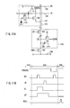
- the second light-shielding layer 2 is applied with a voltage (Vnc) for a switching control of the vertical-signal-line noise-rejection-circuit connection transistor 13.
- the voltage (Vnc) is a pulse voltage as well.
- the voltage (Vnc) is applied as an input signal SP as shown in FIG. 11.
- the second light-shielding layer 2 is used for an output control at the time of outputting an electric signal read out by the reader to the noise rejection circuit 11.
- each of the two layers can be regarded as an independent wiring.
- the freedom degree in a wiring design in an amplification type solid state imaging device can be improved, and thus the wiring structure can be made small and the design cost can be reduced.
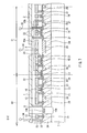
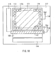
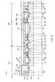
- a first wiring 34 in the fourth embodiment as shown in FIGs. 6 and 7 is connected to the first light-shielding layer 1, and a second wiring 35 is connected to the second light-shielding layer 2.
- a third wiring 36 other than the first wiring 34 and the second wiring 35 is provided in the fourth embodiment.
- the third wiring 36 is connected to the third light-shielding layer 3.
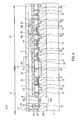
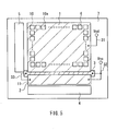
- the amplification type solid state imaging device as shown in FIG. 3 is configured similarly to the amplification type solid state imaging device as shown in FIG. 1.
Landscapes
- Engineering & Computer Science (AREA)
- Multimedia (AREA)
- Signal Processing (AREA)
- Solid State Image Pick-Up Elements (AREA)
- Transforming Light Signals Into Electric Signals (AREA)
Applications Claiming Priority (2)
| Application Number | Priority Date | Filing Date | Title |
|---|---|---|---|
| JP2004322618A JP4652773B2 (ja) | 2004-11-05 | 2004-11-05 | 増幅型固体撮像装置 |
| PCT/JP2005/013732 WO2006048965A1 (ja) | 2004-11-05 | 2005-07-27 | 増幅型固体撮像装置 |
Publications (2)
| Publication Number | Publication Date |
|---|---|
| EP1808894A1 true EP1808894A1 (de) | 2007-07-18 |
| EP1808894A4 EP1808894A4 (de) | 2010-08-04 |
Family
ID=36318982
Family Applications (1)
| Application Number | Title | Priority Date | Filing Date |
|---|---|---|---|
| EP05767155A Withdrawn EP1808894A4 (de) | 2004-11-05 | 2005-07-27 | Halbleiter-bildgebereinrichtung des verstärkungstyps |
Country Status (6)
| Country | Link |
|---|---|
| US (2) | US7830433B2 (de) |
| EP (1) | EP1808894A4 (de) |
| JP (1) | JP4652773B2 (de) |
| CN (1) | CN100502020C (de) |
| TW (1) | TW200629531A (de) |
| WO (1) | WO2006048965A1 (de) |
Cited By (5)
| Publication number | Priority date | Publication date | Assignee | Title |
|---|---|---|---|---|
| WO2011078992A1 (en) * | 2009-12-21 | 2011-06-30 | Omnivision Technologies, Inc. | Image sensor with well bounce correction |
| US8139130B2 (en) | 2005-07-28 | 2012-03-20 | Omnivision Technologies, Inc. | Image sensor with improved light sensitivity |
| US8194296B2 (en) | 2006-05-22 | 2012-06-05 | Omnivision Technologies, Inc. | Image sensor with improved light sensitivity |
| US8274715B2 (en) | 2005-07-28 | 2012-09-25 | Omnivision Technologies, Inc. | Processing color and panchromatic pixels |
| US8416339B2 (en) | 2006-10-04 | 2013-04-09 | Omni Vision Technologies, Inc. | Providing multiple video signals from single sensor |
Families Citing this family (13)
| Publication number | Priority date | Publication date | Assignee | Title |
|---|---|---|---|---|
| JP2009070912A (ja) * | 2007-09-11 | 2009-04-02 | Fujifilm Corp | 固体撮像素子及び撮像装置 |
| JP5159289B2 (ja) * | 2007-12-20 | 2013-03-06 | 株式会社東芝 | 不揮発性半導体記憶装置 |
| JP5111157B2 (ja) | 2008-02-27 | 2012-12-26 | キヤノン株式会社 | 光電変換装置及び光電変換装置を用いた撮像システム |
| KR101776955B1 (ko) * | 2009-02-10 | 2017-09-08 | 소니 주식회사 | 고체 촬상 장치와 그 제조 방법, 및 전자 기기 |
| JP5564874B2 (ja) * | 2009-09-25 | 2014-08-06 | ソニー株式会社 | 固体撮像装置、及び電子機器 |
| JP5810493B2 (ja) * | 2010-09-03 | 2015-11-11 | ソニー株式会社 | 半導体集積回路、電子機器、固体撮像装置、撮像装置 |
| JP2013084713A (ja) * | 2011-10-07 | 2013-05-09 | Sony Corp | 固体撮像素子および製造方法、並びに撮像ユニット |
| JP6071315B2 (ja) * | 2012-08-08 | 2017-02-01 | オリンパス株式会社 | 固体撮像装置および撮像装置 |
| JP6116878B2 (ja) * | 2012-12-03 | 2017-04-19 | ルネサスエレクトロニクス株式会社 | 半導体装置 |
| JP5725123B2 (ja) * | 2013-10-04 | 2015-05-27 | ソニー株式会社 | 固体撮像装置及び電子機器 |
| JP6833470B2 (ja) | 2016-11-17 | 2021-02-24 | キヤノン株式会社 | 固体撮像装置、撮像システム、及び固体撮像装置の製造方法 |
| JP7193907B2 (ja) * | 2017-01-23 | 2022-12-21 | キヤノン株式会社 | 固体撮像装置 |
| JP7335562B2 (ja) | 2020-03-26 | 2023-08-30 | 不二製油株式会社 | 植物性チーズ様食品の製造方法 |
Family Cites Families (21)
| Publication number | Priority date | Publication date | Assignee | Title |
|---|---|---|---|---|
| JPS6185860A (ja) * | 1984-10-03 | 1986-05-01 | Olympus Optical Co Ltd | 固体撮像装置およびその製造方法 |
| DE3705173A1 (de) * | 1986-02-28 | 1987-09-03 | Canon Kk | Halbleitervorrichtung |
| JPS6485860A (en) * | 1987-09-28 | 1989-03-30 | Iseki Agricult Mach | Brake device for vehicle |
| US5115293A (en) | 1989-12-11 | 1992-05-19 | Fuji Photo Film Co., Ltd. | Solid-state imaging device |
| JPH03181169A (ja) * | 1989-12-11 | 1991-08-07 | Fuji Photo Film Co Ltd | 個体撮像装置 |
| JP2757624B2 (ja) * | 1991-10-21 | 1998-05-25 | 日本電気株式会社 | 赤外線固体撮像素子及びその製造方法 |
| JP3181169B2 (ja) | 1994-03-23 | 2001-07-03 | 本田技研工業株式会社 | 内燃機関の空燃比制御装置 |
| US5920418A (en) * | 1994-06-21 | 1999-07-06 | Matsushita Electric Industrial Co., Ltd. | Diffractive optical modulator and method for producing the same, infrared sensor including such a diffractive optical modulator and method for producing the same, and display device including such a diffractive optical modulator |
| JP3219036B2 (ja) * | 1997-11-11 | 2001-10-15 | 日本電気株式会社 | 固体撮像装置 |
| US6977684B1 (en) * | 1998-04-30 | 2005-12-20 | Canon Kabushiki Kaisha | Arrangement of circuits in pixels, each circuit shared by a plurality of pixels, in image sensing apparatus |
| JP3457551B2 (ja) * | 1998-11-09 | 2003-10-20 | 株式会社東芝 | 固体撮像装置 |
| JP3554244B2 (ja) * | 1999-02-25 | 2004-08-18 | キヤノン株式会社 | 光電変換装置及びそれを用いたイメージセンサ並びに画像入力システム |
| US6878977B1 (en) * | 1999-02-25 | 2005-04-12 | Canon Kabushiki Kaisha | Photoelectric conversion device, and image sensor and image input system making use of the same |
| US6043115A (en) * | 1999-03-25 | 2000-03-28 | United Microelectronics Corp. | Method for avoiding interference in a CMOS sensor |
| JP3434740B2 (ja) * | 1999-06-30 | 2003-08-11 | Necエレクトロニクス株式会社 | 固体撮像装置 |
| JP3467013B2 (ja) * | 1999-12-06 | 2003-11-17 | キヤノン株式会社 | 固体撮像装置 |
| JP4236152B2 (ja) * | 2002-07-29 | 2009-03-11 | 富士フイルム株式会社 | 固体撮像素子 |
| US7473977B2 (en) * | 2003-03-06 | 2009-01-06 | Sony Corporation | Method of driving solid state image sensing device |
| KR100690880B1 (ko) * | 2004-12-16 | 2007-03-09 | 삼성전자주식회사 | 픽셀별 광감도가 균일한 이미지 센서 및 그 제조 방법 |
| JP4687155B2 (ja) * | 2005-03-09 | 2011-05-25 | ソニー株式会社 | 固体撮像装置およびその駆動方法 |
| JP4431990B2 (ja) * | 2005-12-14 | 2010-03-17 | ソニー株式会社 | 固体撮像装置 |
-
2004
- 2004-11-05 JP JP2004322618A patent/JP4652773B2/ja not_active Expired - Lifetime
-
2005
- 2005-07-27 CN CNB2005800190132A patent/CN100502020C/zh not_active Expired - Lifetime
- 2005-07-27 EP EP05767155A patent/EP1808894A4/de not_active Withdrawn
- 2005-07-27 WO PCT/JP2005/013732 patent/WO2006048965A1/ja not_active Ceased
- 2005-07-27 US US11/568,565 patent/US7830433B2/en active Active
- 2005-07-29 TW TW094125699A patent/TW200629531A/zh unknown
-
2010
- 2010-08-16 US US12/857,157 patent/US8284283B2/en not_active Expired - Lifetime
Cited By (8)
| Publication number | Priority date | Publication date | Assignee | Title |
|---|---|---|---|---|
| US8139130B2 (en) | 2005-07-28 | 2012-03-20 | Omnivision Technologies, Inc. | Image sensor with improved light sensitivity |
| US8274715B2 (en) | 2005-07-28 | 2012-09-25 | Omnivision Technologies, Inc. | Processing color and panchromatic pixels |
| US8330839B2 (en) | 2005-07-28 | 2012-12-11 | Omnivision Technologies, Inc. | Image sensor with improved light sensitivity |
| US8711452B2 (en) | 2005-07-28 | 2014-04-29 | Omnivision Technologies, Inc. | Processing color and panchromatic pixels |
| US8194296B2 (en) | 2006-05-22 | 2012-06-05 | Omnivision Technologies, Inc. | Image sensor with improved light sensitivity |
| US8416339B2 (en) | 2006-10-04 | 2013-04-09 | Omni Vision Technologies, Inc. | Providing multiple video signals from single sensor |
| WO2011078992A1 (en) * | 2009-12-21 | 2011-06-30 | Omnivision Technologies, Inc. | Image sensor with well bounce correction |
| US8106427B2 (en) | 2009-12-21 | 2012-01-31 | Omnivision Technologies, Inc. | Image sensor with well bounce correction |
Also Published As
| Publication number | Publication date |
|---|---|
| US8284283B2 (en) | 2012-10-09 |
| EP1808894A4 (de) | 2010-08-04 |
| JP4652773B2 (ja) | 2011-03-16 |
| TW200629531A (en) | 2006-08-16 |
| CN1965409A (zh) | 2007-05-16 |
| US20080231733A1 (en) | 2008-09-25 |
| US7830433B2 (en) | 2010-11-09 |
| WO2006048965A1 (ja) | 2006-05-11 |
| US20100309355A1 (en) | 2010-12-09 |
| JP2006135089A (ja) | 2006-05-25 |
| CN100502020C (zh) | 2009-06-17 |
Similar Documents
| Publication | Publication Date | Title |
|---|---|---|
| US8284283B2 (en) | Amplification type solid state imaging device | |
| EP2226844B1 (de) | Festkörperabbildungsvorrichtung, Verfahren zur Herstellung der Festkörperabbildungsvorrichtung und elektronische Vorrichtung | |
| JP3467013B2 (ja) | 固体撮像装置 | |
| US9806120B2 (en) | Solid-state image pickup apparatus and electronic apparatus | |
| US7113215B2 (en) | CMOS image sensor | |
| CN106057840B (zh) | 摄像装置 | |
| JP7641546B2 (ja) | 撮像装置 | |
| US8106342B2 (en) | Solid-state image capturing device and electronic information device | |
| US7800191B2 (en) | Solid-state imaging device and method for driving the same | |
| US20090046186A1 (en) | Solid state image capturing device and electronic information device | |
| US9184208B2 (en) | Solid-state imaging apparatus and electronic device with improved image quality and increased yield | |
| KR101575378B1 (ko) | 고체 촬상 장치 및 이를 포함하는 x선 ct 장치 | |
| US20190288021A1 (en) | Imaging device having photoelectric converters, wiring layer, and capacitor | |
| JP2009118427A (ja) | 固体撮像装置およびその駆動方法 | |
| US7847848B2 (en) | Solid-state imaging device having a plurality of lines formed in at least two layers on semiconductor substrate | |
| JP3916612B2 (ja) | 固体撮像装置、その駆動方法及びそれを用いたカメラ | |
| JP6817605B2 (ja) | 撮像装置 | |
| JP2018050028A (ja) | 固体撮像装置及び電子機器 | |
| KR100861163B1 (ko) | 증폭형 고체 촬상 장치 |
Legal Events
| Date | Code | Title | Description |
|---|---|---|---|
| PUAI | Public reference made under article 153(3) epc to a published international application that has entered the european phase |
Free format text: ORIGINAL CODE: 0009012 |
|
| 17P | Request for examination filed |
Effective date: 20070110 |
|
| AK | Designated contracting states |
Kind code of ref document: A1 Designated state(s): DE FR GB |
|
| RIN1 | Information on inventor provided before grant (corrected) |
Inventor name: MASUYAMA, MASAYUKI,C/O MATSUSHITA EL. IND. CO.,LTD Inventor name: FUJIOKA, TAKASHI,C/O MATSUSHITA EL. IND. CO., LTD. Inventor name: INAGAKI, MAKOTO,C/O MATSUSHITA EL. IND. CO.,LTD. |
|
| DAX | Request for extension of the european patent (deleted) | ||
| RBV | Designated contracting states (corrected) |
Designated state(s): DE FR GB |
|
| RAP1 | Party data changed (applicant data changed or rights of an application transferred) |
Owner name: PANASONIC CORPORATION |
|
| A4 | Supplementary search report drawn up and despatched |
Effective date: 20100701 |
|
| 17Q | First examination report despatched |
Effective date: 20110323 |
|
| STAA | Information on the status of an ep patent application or granted ep patent |
Free format text: STATUS: THE APPLICATION IS DEEMED TO BE WITHDRAWN |
|
| 18D | Application deemed to be withdrawn |
Effective date: 20120120 |