EP1808908B1 - Piezoelektisches Vielschichtbauelement und Herstellungsverfahren dafür - Google Patents
Piezoelektisches Vielschichtbauelement und Herstellungsverfahren dafür Download PDFInfo
- Publication number
- EP1808908B1 EP1808908B1 EP20060256007 EP06256007A EP1808908B1 EP 1808908 B1 EP1808908 B1 EP 1808908B1 EP 20060256007 EP20060256007 EP 20060256007 EP 06256007 A EP06256007 A EP 06256007A EP 1808908 B1 EP1808908 B1 EP 1808908B1
- Authority
- EP
- European Patent Office
- Prior art keywords
- reinforcing layer
- conductive
- conductive reinforcing
- layer
- piezoelectric device
- Prior art date
- Legal status (The legal status is an assumption and is not a legal conclusion. Google has not performed a legal analysis and makes no representation as to the accuracy of the status listed.)
- Not-in-force
Links
Images


Classifications
-
- H—ELECTRICITY
- H10—SEMICONDUCTOR DEVICES; ELECTRIC SOLID-STATE DEVICES NOT OTHERWISE PROVIDED FOR
- H10N—ELECTRIC SOLID-STATE DEVICES NOT OTHERWISE PROVIDED FOR
- H10N30/00—Piezoelectric or electrostrictive devices
- H10N30/80—Constructional details
- H10N30/87—Electrodes or interconnections, e.g. leads or terminals
- H10N30/872—Interconnections, e.g. connection electrodes of multilayer piezoelectric or electrostrictive devices
-
- H—ELECTRICITY
- H10—SEMICONDUCTOR DEVICES; ELECTRIC SOLID-STATE DEVICES NOT OTHERWISE PROVIDED FOR
- H10N—ELECTRIC SOLID-STATE DEVICES NOT OTHERWISE PROVIDED FOR
- H10N30/00—Piezoelectric or electrostrictive devices
- H10N30/01—Manufacture or treatment
- H10N30/06—Forming electrodes or interconnections, e.g. leads or terminals
- H10N30/063—Forming interconnections, e.g. connection electrodes of multilayered piezoelectric or electrostrictive parts
Definitions
- the present invention relates to a multilayer piezoelectric device.
- Piezoelectric devices applied to fuel injection systems have been utilized as power sources for driving injection nozzle opening and closing mechanisms generating displacements and stresses and are mostly used in a state of being contained in cases made of a metal or the like.
- multilayer ones are used as the piezoelectric devices.
- Japanese Patent (Kokai) Publication No. H07-226541A describes that an underlying layer for the external electrodes is bridged to secure conduction.
- Japanese Patent (Kokai) Publication No. H10-229227A describes that a single-layer reinforcement layer is joined to the external electrodes in offset type devices.
- Japanese Utility Model No. 7-22557 discloses a multilayer external electrode structure with an underlying layer and a sequence of layers applied as a metal paste.
- the constraining force of the external electrodes onto the piezoelectric bodies can be reduced by using a flexible material in making the external electrodes or softly joining the external electrodes to the piezoelectric body.
- the constraining force from the external electrodes to the piezoelectric body is reduced, the reliability of the joining sites of the external electrodes to the piezoelectric body tends to be deteriorated after a large number of repetitions of expansion and contraction of the external electrodes; thus, there is an antinomy.
- the present invention provides a multilayer piezoelectric device as set out in claim 1.
- the first conductive reinforcing layer is connected electrically to the underlying layer of the multilayer piezoelectric device, and the second conductive reinforcing layer is joined onto the first conductive reinforcing layer. Moreover, the overlying second conductive reinforcing layer remains free of joining by means of the conductive joining material.
- Such a structure distinctly distinguishes the function of the first conductive reinforcing layer from that of the second conductive reinforcing layer. It is thus possible to successfully provide the two effects which are contradictory to each other, namely improvement in displacement efficiency and improvement in durability.
- the first conductive reinforcing layer to the underlying layer by means of the conductive joining material, it becomes possible to exert a desired constraining force on the laminated body of the device. Since the second conductive reinforcing layer is free of direct joining with the conductive joining material, the constraining force value can be optimized through the designing of the first conductive reinforcing layer.
- the second conductive reinforcing layer with a sufficiently high level of strength, it becomes possible to secure the desired conduction even in such a situation that the underlying layer and the first conductive reinforcing layer undergo disconnection or show increased resistance values.
- a laminated body is constructed by laminating a plurality of piezoelectric layers with one another in the direction of a given axis with internal electrode layers each disposed between the respective two neighboring piezoelectric layers.
- the internal electrode layers are preferably disposed such that the internal electrode layer serving as a positive electrode and the internal electrode layer serving as a negative electrode come one after the other.
- the displacement of the laminated body utilized in the device of the present invention includes all the displacements due to a strain induced in the piezoelectric body by an electric field.
- the device of the invention is not limited to the one utilizing the piezoelectric effect in a narrower sense thereof, namely the one utilizing the piezoelectric effect producing a strain approximately proportional to the intensity of the electric field applied, and to the one utilizing the electrostriction effect producing a strain approximately proportional to the square of the intensity of the electric field applied.
- the device also includes those utilizing such phenomena as polarization inversion generally observed in ferroelectric materials and antiferroelectric phase-ferroelectric phase transition observed in antiferroelectric materials.
- the laminated body constituting the device of the invention can be manufactured by the green sheet lamination method and simultaneous punching/lamination method, although the manufacturing method is not limited thereto.
- An electrode pattern made of a conductive material is formed on each of green sheets mainly made of a piezoelectric material, green sheets with the electrode pattern formed thereon are punched while laminating them on the punch of a punching machine utilizing the punch as the lamination axis.
- the thus-obtained green laminated body is fired to give a columnar laminated body integrated by firing.
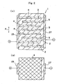
- Fig. 1 (a) shows a schematic perspective view of a laminated body 1 utilizable in producing the device of the invention
- Fig. 1 (b) shows a perspective view showing the pattern of internal electrode layers on the respective piezoelectric layers.
- Fig. 2 (a) is a schematic longitudinal sectional view of the laminated body
- Fig. 2 (b) is a schematic transverse sectional view of the laminated body of Fig. 2 (a) .
- a number of piezoelectric layers 2 are piled up in the direction of the given axis "A", and an internal electrode layer 4 or 5 is formed between each pair of neighboring piezoelectric layers 2.
- a plus polarity voltage is applied to each internal electrode layer 4, whereas a minus polarity voltage is applied to each internal electrode layer 5.
- the internal electrode layers 4 and 5 are formed alternately and, as shown in Fig. 1 (b) , the internal electrode layers 4 and 5 differ in the planar patterns from each other.
- This kind of device is called "offset multilayer piezoelectric device". It is to be noted, however, that the present invention is not limited to such offset multilayer piezoelectric devices.
- Each internal electrode layer 4 is electrically connected to an electrode structure 23, and each internal electrode layer 5 is electrically connected to another electrode structure 27. Each electrode structure will be described later herein.
- the green sheet lamination method and simultaneous punching/lamination method are preferably utilized.
- a predetermined number of ceramic-made green sheets mainly made of a piezoelectric/electrostriction material are prepared. These ceramic green sheets constitute piezoelectric layers after firing.
- Such ceramic green sheets can be prepared by those ceramic manufacturing methods known in the art. For example, powder of a piezoelectric/electrostriction material is prepared, an organic resin (binder), a solvent, a dispersant and a plasticizer, among others, are admixed therewith according to a desired formulation, the thus-prepared slurry is subjected to degassing treatment. The slurry is then molded by such a tape forming method as the doctor blade method, reverse roll coater method or reverse doctor roll coater method, and the thus formed tape is cut, whereby the desired sheets can be prepared.
- a tape forming method as the doctor blade method, reverse roll coater method or reverse doctor roll coater method
- the piezoelectric (electrostriction) material is not particularly restricted but may be any material capable of causing an electric field-induced strain. It may be either crystalline or noncrystalline, and it is also possible to use semiconductor ceramic materials, ferroelectric ceramic materials or antiferroelectric ceramic materials. The material may be properly selected for utilization according to the intended use. The material may be one requiring polarization treatment or one not requiring polarization treatment.
- BNT bismuth neodymium titanate
- These materials may contain one or more of the oxide(s) of lanthanum, calcium, strontium, molybdenum, tungsten, barium, niobium, zinc, nickel, manganese, cerium, cadmium, chromium, cobalt, antimony, iron, yttrium, tantalum, lithium, bismuth, tin, copper and so forth, each as a solute in the solid solution.
- a conductor membrane having a predetermined pattern is formed on the surface of each sheet using a conductive material.
- This conductor membrane is a membrane to serve later as an internal electrode layer.
- a screen printing method is preferably used. Such means as photolithography, transfer printing or stamping may also be used.
- the conductive material to be used are metals occurring as solids at room temperature.
- metals such as aluminum, titanium, chromium, iron, cobalt, nickel, copper, zinc, niobium, molybdenum, ruthenium, palladium, rhodium, silver, tin, tantalum, tungsten, iridium, platinum, gold and lead, and alloys composed of two or more of these, for example silver-platinum, platinum-palladium and silver-palladium, either singly or in combination of two or more species.
- cermets resulting from admixing the materials mentioned above with aluminum oxide, zirconium oxide, titanium oxide, silicon oxide, cerium oxide, glass, or a piezoelectric/electrostriction material, for instance, may also be used.
- the conductive material is selected from among these materials depending on whether it can be fired simultaneously with the piezoelectric/electrostriction layers. In the case of internal electrode layers, they are fired simultaneously with the piezoelectric/electrostriction layers and, therefore, it is necessary to use a high-melting metal which will not change or melt at the temperature for firing the piezoelectric/electrostriction layers, for example platinum, palladium, a platinum-palladium alloy or a silver-palladium alloy.
- the conductor layers to serve later as underlying layers they are formed after firing of the laminated body and therefore can be fired at a lower temperature as compared with the temperature for firing the piezoelectric body.
- a predetermined number of sheets each with a conductor membrane to later serve as an internal electrode layer as formed thereon are subjected to punching processing using a punching machine with the clearance between the punch and die properly adjusted, while laminating the processed sheets on the punch utilizing the punch as the lamination axis, as already mentioned hereinabove.
- the resulting sheets are then laminated with pressure bonding to give a green laminated body. This green laminated body is fired to give an integrated laminated (fired) body.
- a conductive underlying layer is disposed on each or both of the two side or lateral faces 30 of the laminated body (cf. Fig. 1 ), and the underlying layers are electrically connected to the corresponding internal electrodes.
- the side faces 30 of a laminated body it is meant that the plane of the side face is substantially parallel to the direction "A" of expansion and contraction of the piezoelectric body. The normal line of the side face is substantially perpendicular to the direction "A”.
- a first conductive reinforcing layer and a second conductive reinforcing layer are combined together and the combined reinforcement layer assembly is joined onto each underlying layer formed on the fired piezoelectric body. In this case, care is taken so that the second conductive reinforcing layer may not be joined by means of the conductive joining material.
- the screen printing method is properly used but such means as photolithography, transfer or stamping may also be used.
- the conductive material to be used are metals occurring as solids at room temperature.
- metals such as aluminum, titanium, chromium, iron, cobalt, nickel, copper, zinc, niobium, molybdenum, ruthenium, palladium, rhodium, silver, tin, tantalum, tungsten, iridium, platinum, gold and lead, and alloys composed of two or more of these, for example silver-platinum, platinum-palladium and silver-palladium, either singly or in combination of two or more species.
- Mixtures or cermets resulting from admixing the materials mentioned above with aluminum oxide, zirconium oxide, titanium oxide, silicon oxide, cerium oxide, glass, or a piezoelectric/electrostriction material, for instance, may also be used.
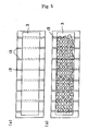
- Fig. 3 is a cross-sectional view showing the principal portions of a device according to an embodiment of the invention.
- the laminated body 1 comprises a number of piezoelectric layers 2 laminated in the direction of the arrow "A".
- An internal electrode layer 4 or 5 is formed between each pair of neighboring piezoelectric layers.
- Each internal electrode layer 4 is electrically connected to the underlying layer 3.
- the underlying layer 3 is joined to the first conductive reinforcing layer 10 by means of the conductive joining material 9, and the first conductive reinforcing layer 10 is joined to the second conductive reinforcing layer 11.
- a composite conductive reinforcing layer 12 is formed by the first conductive reinforcing layer and the second conductive reinforcing layer.
- the second conductive reinforcing layer 11 is not wetted with the conductive joining material 9 and therefore is not directly joined to the underlying layer.
- the method of joining the first conductive reinforcing layer and the second conductive reinforcing layer together is not particularly restricted.
- both layers are combined by welding, diffusion bonding or brazing or by using a conductive adhesive.
- Such methods of bonding are well known in the field of metal processing.
- each first conductive reinforcing layer is made of a sheet-shaped metal.
- the first conductive reinforcing layer can be made relatively thin and the constraining force can be reduced, so that the laminated body can show an increased displacement.
- the first conductive reinforcing layer is preferably not thicker than 500 ⁇ m, more preferably not thicker than 250 ⁇ m.
- the layer is preferably not thinner than 10 ⁇ m, more preferably not thinner than 30 ⁇ m.
- the first conductive reinforcing layer may be a sheet-like matter substantially lacking in elasticity. In this case, the displacement of the laminated body can be increased by further reducing the thickness of the sheet-like matter.
- the sheet-like matter constituting the first conductive reinforcing layer is made of an expanded metal, punched metal or etched metal.
- the material constituting the first conductive reinforcing layer is not particularly restricted but may be any of the materials having desired levels of Young's modulus, strength and conductivity.
- the material of the first conductive reinforcing layer comprises at least one metal selected from the group consisting of Ni, Cu, Fe, Cr, Ti, Mg, Al, Ag, Pd, Pt and Au, and the alloys of these. Among them, the following are particularly preferred: from the cost viewpoint, Ni, Cu and Ti are desirable.
- Cu which is a material low in Young's modulus and low in resistance, can be said to be an excellent material.
- the second conductive reinforcing layer from the viewpoint of increasing the displacement of the laminated body, a net-like material is used.
- the material of the second conductive reinforcing layer is not particularly restricted but may be any of those materials with which desired levels of Young's modulus, strength and conductivity can be realized.
- the material comprises at least one metal selected from the group consisting of Ni, Cu, Fe, Cr, Ti, Mg, Al, Ag, Pd, Pt and Au, and the alloys of these.
- the percentage open area of the first conductive reinforcing layer is preferably larger than that of the second conductive reinforcing layer. Thereby, it becomes possible to reduce the constraint of the laminated body by the first conductive reinforcing layer and thereby increase the displacement. Further, it becomes easy to secure the electric conduction by the second conductive reinforcing layer in case of the first conductive reinforcing layer being disconnected or showing an increased resistance value. From this viewpoint, the difference in percentage open areas between the first conductive reinforcing layer and second conductive reinforcing layer is preferably not smaller than 5%, more preferably not smaller than 10%.
- the percentage open area of the first conductive reinforcing layer is preferably not smaller than 40%, more preferably not smaller than 50%. From the viewpoint of securing the conduction, the percentage open area of the first conductive reinforcing layer is preferably not larger than 75%.
- the percentage open area of the second conductive reinforcing layer is preferably not smaller than 10%, more preferably not smaller than 25%. From the viewpoint of securing the conduction, the percentage open area of the second conductive reinforcing layer is preferably not larger than 60%.
- the area of the conductive joining material is made larger than that of the first conductive reinforcing layer.
- the material constituting the conductive joining material is not particularly restricted but may be any of the materials capable of joining the first conductive reinforcing layer.
- the material comprises at least one metal selected from the group consisting of Sn, Pb, Cu, Ag, Au, In, Ga and Al, and the alloys thereof. Particularly preferred are the materials mentioned below.
- solder alloys derived from Sn-Pb eutectic alloys doped with Ag and of such Pb-free solders as Sn-3Ag-0.5Cu, Sn-8Zn-3Bi and Sn-7Zn-0.003Al alloys.
- Sn-3Ag-0.5Cu alloy is desirable in view of its high connection reliability.
- the material M705 (inventory number) available from Senju Metal Industry Co., Ltd. is preferred.
- the second conductive reinforcing layers are each substantially free of joining by the conductive joining material. This situation includes the following two forms.
- At least 10% but not larger than 70% of the surface area of the conductive reinforcing layer is in contact with the conductive joining material.
- at least 10% of the surface area of the conductive reinforcing layer with the conductive joining material it becomes possible to make the adhesion firm and to prevent the first conductive reinforcing layer from peeling off.
- By contacting not larger than 50% of the surface area of the conductive reinforcing layer with the conductive joining material it becomes possible to increase the displacement of the laminated body.
- the second conductive reinforcing layer is joined to the first conductive reinforcing layer at points of intersection of the first conductive reinforcing layer.
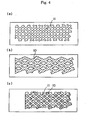
- Fig. 4 (a) is a plan view showing a net-like matter 11 constituting the second conductive reinforcing layer
- Fig. 4 (b) is a plan view showing an expanded metal (or punched metal) 10 constituting the first conductive reinforcing layer.
- the second conductive reinforcing layer 11 is placed on the first conductive reinforcing layer 10 and the both are joined together to prepare a composite conductive reinforcing layer 12.
- the first conductive reinforcing layer 10 is joined to the second conductive reinforcing layer 11 at the points of intersection of the first conductive reinforcing layer 10.
- conductor connecting sites 13 connected to respective internal electrode layers 4 are exposed on a side of the laminated body 1 and the conductor connecting sites 13 are connected to the underlying layer 3.
- the composite conductive reinforcing layer 12 is placed on and joined to the underlying layer 3.
- the underlying layer 3 is joined to the first conductive reinforcing layer 10A via the conductive joining material 9, and the first conductive reinforcing layer 10A is joined to the second conductive reinforcing layer 11A.
- a composite conductive reinforcing layer 12A is formed by the first conductive reinforcing layer 10A and second conductive reinforcing layer 11A.
- the second conductive reinforcing layer 11A is not wetted with the conductive joining material 9; therefore, it is not directly joined to the underlying layer 3.
- the device according to the invention is applicable as a multilayer capacitor, a multilayer piezoelectric device or the like.
- Multilayer capacitors are capacitors currently used most frequently, in most of electric and electronic circuits in various kinds of products. They are suited for use, for example, in computers, communications apparatus, or portable terminal units, such as cellular phones, which are required to be small in size and light in weight.
- the multilayer piezoelectric device is used as a piezoelectric device such as a sensor or actuator in a measurement apparatus, optical modulator, optical switch, electric switch, microrelay, microvalve, transport mechanism, display, projector or like image display device, image drawing device, micropump, liquid drop discharging device, micromixer, microstirrer or microreactor, for instance.
- the device of the invention is used as a favorable driving source for actuating an injection nozzle opening/closing mechanism in a fuel injection system. It is also applied as a driving source for an apparatus requiring precise positioning, such as an optical apparatus, or for vibration control equipment.
- a device shown in Figs. 1-3 was constructed. Specifically, 300-350 layers for constituting an active region and 50 layers each for constituting the upper or lower inactive regions were integrated by lamination. An internal electrode layer (e.g. 3 ⁇ m in thickness) was printed on each section of a piezoelectric tape and an adhesive layer (e.g. 5 ⁇ m in thickness) with an increased binder content as compared with the tape was printed thereon, and the layers were integrated by heating at 80°C and weighting at 2 MPa.
- An internal electrode layer e.g. 3 ⁇ m in thickness
- an adhesive layer e.g. 5 ⁇ m in thickness
- the thus-integrated laminated molding was degreased at 600°C and fired at 900-1100°C to give a laminated piezoelectric ceramics body.
- This laminated body was cut and ground smooth to give a laminated body having a desired shape.
- the cross-section of the laminated body was 7 mm x 7 mm in size and the length thereof was 35 mm.
- An underlying layer 3 to serve as an external electrode was formed on each of two sides of the device with offset electrode layers drawn out.
- a fired AgPd membrane was bound to each side by baking at 800°C; the thickness of the membrane baked was 20 ⁇ m.
- a multilayer mesh member was joined to each underlying layer.
- a multilayer mesh 12 was prepared by integrating an expanded metal 10 made of Cu and a SUS mesh 11 by diffusion bonding and joined to the underlying layer 3 using a solder 9.
- solder Used as the solder was a Sn-Ag-Cu alloy-based Pb-free solder, and the joining was carried out under the conditions of 240°C and 5 minutes.
- the whole device was coated with an insulating resin. Specifically, the device was selectively coated by applying an epoxy resin and a fluororesin.
- the resin thickness was 20-100 ⁇ m.
- the device was polarized. Specifically, a DC voltage of 150 V was applied for 10 minutes and then a DC voltage of 240 V for 10 minutes, in a condition heated at 170°C, to complete the polarization.
- the intensities of the electric fields on that occasion corresponded to 1.9 kV/mm and 3.0 kV/mm, respectively.
- the device was actuated by applying a voltage of 200 V under a preload of 750 N.
- the waveform applied was 0.12 msec in rise time, 1 msec in keep time and 0.12 msec in fall time.
- the displacement of the device that could be attained was 50 ⁇ m.
- the multilayer reinforcing layer structure according to the invention made it possible to reduce the constraining force of each external electrode, and the element obtained was excellent in durability. Even after 1 billion cycles, no breakage was observed.
- a device 20 schematically shown in Fig. 7 was constructed. Specifically, 300-350 layers for constituting an active region and 50 layers each for constituting the upper or lower inactive region were integrated by lamination. An internal electrode layer (e.g. 3 ⁇ m in thickness) was printed on each section of a piezoelectric tape and an adhesive layer (e.g. 5 ⁇ m in thickness) with an increased binder content as compared with the tape was printed thereon. The layers were integrated by heating at 80°C and weighting at 2 MPa.
- the thus-integrated laminated molding was degreased at 600°C and fired at 900-1100°C to give a laminated piezoelectric ceramics body.
- This laminated body was cut and ground smooth to give a laminated body having a desired shape.
- the cross-section of the laminated body was 7 mm x 7 mm in size and the length thereof was 35 mm.
- An underlying layer 15 to serve as an external electrode was formed on each of two sides of the device with offset electrode layers drawn out.
- a fired AgPd membrane was bound to each side by baking at 800°C; the thickness of the membrane baked was 20 ⁇ m. No external electrode reinforcing member was joined to the element.
- the whole device was coated with an insulating resin. Specifically, the device was selectively coated by applying an epoxy resin and a fluororesin.
- the resin thickness was 20-100 ⁇ m.
- the element was polarized. Specifically, a DC voltage of 150 V was applied for 10 minutes and then a DC voltage of 240 V for 10 minutes, in a condition heated at 170°C, to complete the polarization.
- the intensities of the electric fields on that occasion corresponded to 1.9 kV/mm and 3.0 kV/mm, respectively.
- the device was actuated by applying a voltage of 200 V under a preload of 750 N.
- the waveform applied was 0.12 msec in rise time, 1 msec in keep time and 0.12 msec in fall time.
- the displacement of the device that could be attained was 50 ⁇ m. After 10 thousand actuation cycles, cracking occurred within the device and one of the external electrode layers was cut apart thereby, and the element stopped functioning.
- a device shown in Fig. 8 was constructed. Specifically, a laminated body 1 and underlying layers 3 were formed in the same manner as in Comparative Example 1. Then, a SUS mesh 11 was joined to each underlying layer 3 by soldering. However, the form of joining was such that the SUS mesh 11 was embedded in the solder 19.
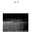
- the appearance of the device constructed in Example 1 is shown in Fig. 9
- a cross-section thereof is shown in Fig. 10 .
- the net-shaped second conductive reinforcing layer is exposed on the device surface.
- the underlying layer is formed on the laminated body surface, and the first conductive reinforcing layer is protruding from the underlying layer through the conductive material, and the second conductive reinforcing layer is bonded thereto. There is a gap between the second conductive reinforcing layer and the joining material.
- Fig. 11 is a graphic representation of the relations between number of actuation cycles and actuator displacement for the devices of Example 1 and Comparative Examples 1 and 2.
Landscapes
- Engineering & Computer Science (AREA)
- Manufacturing & Machinery (AREA)
- General Electrical Machinery Utilizing Piezoelectricity, Electrostriction Or Magnetostriction (AREA)
- Impact Printers (AREA)
- Micromachines (AREA)
Claims (15)
- Mehrschichtige piezoelektrische Vorrichtung, umfassend:einen Laminatkörper (1), der eine Vielzahl an piezoelektrischen Schichten (2), die in Richtung einer vorgegebenen Achse laminiert sind, und interne Elektrodenschichten (4, 5), die jeweils zwischen zwei benachbarten piezoelektrischen Schichten angeordnet sind;eine Unterschicht (3), die auf einer Seitenfläche des Laminatkörpers angeordnet ist und elektrisch mit den internen Elektrodenschichten verbunden ist;eine erste leitfähige Verstärkungsschicht (10), die mit der Unterschicht (3) verbunden ist;eine zweite leitfähige Verstärkungsschicht (11), die mit der ersten leitfähigen Verstärkungsschicht (10) verbunden ist; undein leitfähiges Verbindungsmaterial (9), das die Unterschicht (3) und die erste leitfähige Verstärkungsschicht (10) verbindet, umfasst,worin die zweite leitfähige Verstärkungsschicht (11) frei von einer Verbindung mittels des leitfähigen Verbindungsmaterials (9) ist, dadurch gekennzeichnet, dass die zweite leitfähige Verstärkungsschicht (11) ein Netz umfasst oder ein netzartiges Material ist.
- Piezoelektrische Vorrichtung nach Anspruch 1, worin die erste leitfähige Verstärkungsschicht (10) und die zweite leitfähige Verstärkungsschicht (11) durch Schweißen, Diffusionsschweißen, Löten oder einen leitfähigen Kleber miteinander verbunden sind.
- Piezoelektrische Vorrichtung nach einem der Ansprüche 1 oder 2, worin die erste leitfähige Verstärkungsschicht (10) ein plattenförmiges Metall umfasst.
- Piezoelektrische Vorrichtung nach Anspruch 3, worin das plattenförmige Metall ein flaches Blech umfasst.
- Piezoelektrische Vorrichtung nach Anspruch 3, worin das plattenförmige Metall ein Streckmetall, ein gestanztes Metall oder ein geätztes Blech ist.
- Piezoelektrische Vorrichtung nach einem der Ansprüche 1 bis 5, worin die erste leitfähige Verstärkungsschicht (10) zumindest ein aus Ni, Cu, Fe, Cr, Ti, Mg, Al, Ag, Pd, Pt, Au und den Legierungen davon ausgewähltes Metall umfasst.
- Piezoelektrische Vorrichtung nach einem der Ansprüche 1 bis 6, worin die zweite leitfähige Verstärkungsschicht (11) zumindest ein aus Ni, Cu, Fe, Cr, Ti, Mg, Al, Ag, Pd, Pt, Au und den Legierungen davon ausgewähltes Metall umfasst.
- Piezoelektrische Vorrichtung nach einem der Ansprüche 1 bis 5, worin die erste leitfähige Verstärkungsschicht (10) prozentual eine größere freie Fläche aufweist als die zweite leitfähige Verstärkungsschicht (11).
- Piezoelektrische Vorrichtung nach einem der Ansprüche 1 bis 8, worin das leitfähige Verbindungsmaterial (9) eine größere Fläche aufweist als die erste leitfähige Verstärkungsschicht (10).
- Piezoelektrische Vorrichtung nach einem der Ansprüche 1 bis 9, worin das leitfähige Verbindungsmaterial zumindest ein aus Sn, Pb, Cu, Ag, Au, In, Ga und Al ausgewähltes Material umfasst.
- Piezoelektrische Vorrichtung nach einem der Ansprüche 1 bis 10, worin das leitfähige Verbindungsmaterial (9) einen organischen Kleber umfasst, der eine leitfähige Substanz enthält.
- Piezoelektrische Vorrichtung nach einem der Ansprüche 1 bis 11, worin 10 % bis 80 % der Oberfläche der ersten leitfähigen Verstärkungsschicht (10) in Kontakt mit dem leitfähigen Verbindungsmaterial (9) stehen.
- Piezoelektrische Vorrichtung nach einem der Ansprüche 1 bis 5, worin die erste leitfähige Verstärkungsschicht (10) mit der zweiten leitfähigen Verstärkungsschicht (11) an Schnittpunkten mit der ersten leitfähigen Verstärkungsschicht (10) verbunden ist.
- Piezoelektrische Vorrichtung nach einem der Ansprüche 1 bis 13 zur Verwendung als Antriebsquelle zur Betätigung eines Einspritzdüsen-Öffnungs/Schließmechanismus in einem internen Motor-Kraftstoffeinspritzsystem.
- Verfahren zur Herstellung einer mehrschichtigen piezoelektrischen Vorrichtung, wobei die Vorrichtung einen Laminatkörper (1), der eine Vielzahl an piezoelektrischen Schichten (2), die in Richtung einer vorgegebenen Achse laminiert sind, und interne Elektrodenschichten (4, 5), die jeweils zwischen zwei benachbarten piezoelektrischen Schichten angeordnet sind; eine Unterschicht (3), die auf einer Seitenfläche des Laminatkörpers angeordnet ist und elektrisch mit den internen Elektrodenschichten verbunden ist; eine erste leitfähige Verstärkungsschicht (10), die mit der Unterschicht (3) verbunden ist; eine zweite leitfähige Verstärkungsschicht (11), die mit der ersten leitfähigen Verstärkungsschicht (10) verbunden ist; und ein leitfähiges Verbindungsmaterial (9), das die Unterschicht (3) und die erste leitfähige Verstärkungsschicht (10) verbindet, umfasst,
worin die zweite leitfähige Verstärkungsschicht (11) ein Netz umfasst oder ein netzartiges Material ist,
wobei das Verfahren folgende Schritte umfasst:das Verbinden der ersten leitfähigen Verstärkungsschicht (10) mit der zweiten leitfähigen Verstärkungsschicht (11); undanschließend das Verbinden der ersten leitfähigen Verstärkungsschicht (10) mit der Unterschicht (3) mittels des leitfähigen Verbindungsmaterials (9), um zu verhindern, dass die zweite leitfähige Verstärkungsschicht (11) mittels des leitfähigen Verbindungsmaterials (9) mit der Unterschicht (3) verbunden wird.
Applications Claiming Priority (1)
| Application Number | Priority Date | Filing Date | Title |
|---|---|---|---|
| JP2006006484A JP4936306B2 (ja) | 2006-01-13 | 2006-01-13 | 積層型圧電素子およびその製造方法 |
Publications (3)
| Publication Number | Publication Date |
|---|---|
| EP1808908A2 EP1808908A2 (de) | 2007-07-18 |
| EP1808908A3 EP1808908A3 (de) | 2008-04-09 |
| EP1808908B1 true EP1808908B1 (de) | 2010-01-06 |
Family
ID=37734049
Family Applications (1)
| Application Number | Title | Priority Date | Filing Date |
|---|---|---|---|
| EP20060256007 Not-in-force EP1808908B1 (de) | 2006-01-13 | 2006-11-23 | Piezoelektisches Vielschichtbauelement und Herstellungsverfahren dafür |
Country Status (4)
| Country | Link |
|---|---|
| US (1) | US7538475B2 (de) |
| EP (1) | EP1808908B1 (de) |
| JP (1) | JP4936306B2 (de) |
| DE (1) | DE602006011570D1 (de) |
Families Citing this family (27)
| Publication number | Priority date | Publication date | Assignee | Title |
|---|---|---|---|---|
| US7786652B2 (en) * | 2004-03-29 | 2010-08-31 | Kyocera Corporation | Multi-layer piezoelectric element |
| US7385337B2 (en) * | 2004-06-18 | 2008-06-10 | Tdk Corporation | Multilayer piezoelectric element |
| DE102004057795B4 (de) * | 2004-11-30 | 2006-12-28 | Siemens Ag | Kontaktierung von Vielschicht-Piezoaktoren bzw. -sensoren |
| DE102006006077B4 (de) * | 2006-02-09 | 2009-04-09 | Continental Automotive Gmbh | Piezokeramischer Vielschicht-Aktor, Verfahren zum Herstellen eines piezokeramischen Vielschicht-Aktors und Einspritzsystem |
| US7545084B2 (en) * | 2006-07-20 | 2009-06-09 | Ngk Insulators, Ltd. | Piezoelectric/electrostrictive ceramic composition, piezoelectric/electrostrictive device, and method of producing the same |
| CN101897049B (zh) * | 2007-11-14 | 2013-12-18 | 怡德乐纳斯公司 | 具有结合焊带的平面弹簧组件及其制造方法 |
| CN101911325B (zh) * | 2007-12-26 | 2013-05-15 | 京瓷株式会社 | 层叠型压电元件、利用该元件的喷射装置及燃料喷射系统 |
| EP2259352B1 (de) * | 2008-04-11 | 2012-08-29 | Murata Manufacturing Co. Ltd. | Beschichteter piezoelektrischer aktuator |
| JPWO2009130863A1 (ja) * | 2008-04-21 | 2011-08-11 | 株式会社村田製作所 | 積層型圧電アクチュエータ |
| DE102008062021A1 (de) * | 2008-08-18 | 2010-03-04 | Epcos Ag | Piezoaktor in Vielschichtbauweise |
| JP2010103250A (ja) * | 2008-10-22 | 2010-05-06 | Taiheiyo Cement Corp | 圧電アクチュエータ |
| JP2010103249A (ja) * | 2008-10-22 | 2010-05-06 | Taiheiyo Cement Corp | 圧電アクチュエータ |
| JP2010103251A (ja) * | 2008-10-22 | 2010-05-06 | Taiheiyo Cement Corp | 圧電アクチュエータ |
| DE102008056746A1 (de) | 2008-11-11 | 2010-05-12 | Epcos Ag | Piezoaktor in Vielschichtbauweise und Verfahren zur Befestigung einer Außenelektrode bei einem Piezoaktor |
| EP2359419B1 (de) * | 2008-11-20 | 2013-01-09 | CeramTec GmbH | Vielschichtaktor mit aussenelektroden als metallische, poröse, dehnbare leitschicht |
| CN102341928B (zh) * | 2009-03-04 | 2014-03-19 | 京瓷株式会社 | 层叠型压电元件、具备其的喷射装置以及燃料喷射系统 |
| DE102010049574A1 (de) * | 2010-07-30 | 2012-02-02 | Epcos Ag | Piezoelektrischer Vielschichtaktor |
| JP5604251B2 (ja) * | 2010-09-30 | 2014-10-08 | 太平洋セメント株式会社 | 圧電素子 |
| DE102010042969A1 (de) * | 2010-10-26 | 2012-04-26 | Continental Automotive Gmbh | Piezoelektrisches Bauteil mit Kontaktierung |
| JP5787547B2 (ja) * | 2011-02-23 | 2015-09-30 | 京セラ株式会社 | 積層型圧電素子およびこれを備えた噴射装置ならびに燃料噴射システム |
| WO2013065709A1 (ja) * | 2011-10-31 | 2013-05-10 | 京セラ株式会社 | 積層型圧電素子およびこれを備えた圧電アクチュエータ、噴射装置、燃料噴射システム |
| JP5842635B2 (ja) * | 2012-01-27 | 2016-01-13 | Tdk株式会社 | 積層型圧電素子 |
| CN104334498B (zh) * | 2012-04-16 | 2016-12-21 | 佳能株式会社 | 铌酸钠粉末及其制备方法、陶瓷制备方法及压电元件 |
| DE102012020956A1 (de) * | 2012-10-25 | 2014-04-30 | Feindrahtwerk Adolf Edelhoff Gmbh & Co. Kg | Drahtgelege, Piezoelement mit Drahtgelege und Herstellungsverfahren |
| DE102013102278A1 (de) * | 2013-03-07 | 2014-09-11 | Epcos Ag | Kondensatoranordnung |
| US10283271B2 (en) * | 2014-01-17 | 2019-05-07 | Kyocera Corporation | Laminated electronic component and laminated electronic component mounting structure |
| JP6907493B2 (ja) * | 2016-09-28 | 2021-07-21 | ブラザー工業株式会社 | アクチュエータ装置、配線部材の接続構造、液体吐出装置、及び、アクチュエータ装置の製造方法 |
Family Cites Families (18)
| Publication number | Priority date | Publication date | Assignee | Title |
|---|---|---|---|---|
| US5406164A (en) * | 1993-06-10 | 1995-04-11 | Brother Kogyo Kabushiki Kaisha | Multilayer piezoelectric element |
| JPH0722557A (ja) | 1993-07-02 | 1995-01-24 | Nomura Seimitsu Denshi Kk | Icリードフレーム及びその部分めっき方法 |
| JPH0722557U (ja) * | 1993-09-21 | 1995-04-21 | 住友金属工業株式会社 | 積層型圧電部品の外部電極 |
| JPH07226541A (ja) | 1994-02-09 | 1995-08-22 | Brother Ind Ltd | 積層型圧電素子 |
| DE19648545B4 (de) | 1996-11-25 | 2009-05-07 | Ceramtec Ag | Monolithischer Vielschichtaktor mit Außenelektroden |
| DE19715488C1 (de) * | 1997-04-14 | 1998-06-25 | Siemens Ag | Piezoaktor mit neuer Kontaktierung und Herstellverfahren |
| JP3262048B2 (ja) * | 1997-10-01 | 2002-03-04 | 株式会社村田製作所 | 圧電共振子およびそれを用いた電子部品 |
| DE19753930A1 (de) | 1997-12-05 | 1999-06-10 | Ceramtec Ag | Verfahren zur Anbringung von Außenelektroden an Festkörperaktoren |
| DE19913271A1 (de) * | 1999-03-24 | 2000-09-28 | Bosch Gmbh Robert | Piezoelektrischer Aktor |
| DE19928189A1 (de) | 1999-06-19 | 2001-04-19 | Bosch Gmbh Robert | Piezoaktor |
| DE19928190A1 (de) | 1999-06-19 | 2001-01-11 | Bosch Gmbh Robert | Piezoaktor |
| EP1110252A1 (de) | 1999-06-23 | 2001-06-27 | Robert Bosch Gmbh | Vielschicht-piezoaktuator mit verbessertem elektrodenkontakt |
| JP4158338B2 (ja) | 2000-06-06 | 2008-10-01 | 株式会社デンソー | インジェクタ用圧電体素子 |
| DE10152490A1 (de) | 2000-11-06 | 2002-05-08 | Ceramtec Ag | Außenelektroden an piezokeramischen Vielschichtaktoren |
| JP3964184B2 (ja) | 2000-12-28 | 2007-08-22 | 株式会社デンソー | 積層型圧電アクチュエータ |
| JP3667289B2 (ja) * | 2001-02-27 | 2005-07-06 | 京セラ株式会社 | 積層型圧電素子及びその製法並びに噴射装置 |
| DE10206115A1 (de) * | 2001-03-06 | 2002-09-19 | Ceramtec Ag | Piezokeramische Vielschichtaktoren sowie ein Verfahren zu ihrer Herstellung |
| JP4876467B2 (ja) * | 2004-12-06 | 2012-02-15 | 株式会社デンソー | 積層型圧電素子 |
-
2006
- 2006-01-13 JP JP2006006484A patent/JP4936306B2/ja not_active Expired - Fee Related
- 2006-11-21 US US11/602,778 patent/US7538475B2/en not_active Expired - Fee Related
- 2006-11-23 DE DE200660011570 patent/DE602006011570D1/de active Active
- 2006-11-23 EP EP20060256007 patent/EP1808908B1/de not_active Not-in-force
Also Published As
| Publication number | Publication date |
|---|---|
| EP1808908A2 (de) | 2007-07-18 |
| JP4936306B2 (ja) | 2012-05-23 |
| US7538475B2 (en) | 2009-05-26 |
| EP1808908A3 (de) | 2008-04-09 |
| DE602006011570D1 (de) | 2010-02-25 |
| US20070164639A1 (en) | 2007-07-19 |
| JP2007189099A (ja) | 2007-07-26 |
Similar Documents
| Publication | Publication Date | Title |
|---|---|---|
| EP1808908B1 (de) | Piezoelektisches Vielschichtbauelement und Herstellungsverfahren dafür | |
| CN100563039C (zh) | 叠层型压电元件及其制造方法 | |
| JP3501860B2 (ja) | 圧電/電歪膜型素子及びその製造方法 | |
| EP1089352B1 (de) | Piezoelektrisches/elektrostriktives Bauelement und dessen Herstellungsverfahren | |
| US7372191B2 (en) | Microswitch and method for manufacturing the same | |
| US6448691B1 (en) | Piezoelectric/electrostrictive device and method of manufacturing same | |
| JP2665106B2 (ja) | 圧電/電歪膜型素子 | |
| JP2002202024A (ja) | インジェクタ用圧電体素子 | |
| JPH0412678A (ja) | 圧電/電歪膜型アクチュエータの製造方法 | |
| EP2056442B1 (de) | Piezoelektrisches aktorelement für einen ultraschallmotor | |
| CN101188270A (zh) | 层叠型压电元件 | |
| CZ2001578A3 (cs) | Piezoelektrický ovladač | |
| JPH08242025A (ja) | 圧電アクチュエータ | |
| JP2001267646A (ja) | 積層型圧電アクチュエータ | |
| US6844659B2 (en) | Wiring board and method of manufacturing same | |
| JP2004363489A (ja) | 圧電/電歪素子、圧電/電歪素子の製造方法、圧電/電歪デバイス及び圧電/電歪デバイスの製造方法 | |
| EP2234184B1 (de) | Verfahren zur Herstellung eines piezoelektrischen Aktuators | |
| JP5201646B2 (ja) | 積層型圧電素子 | |
| JP2004274029A (ja) | 圧電アクチュエータ | |
| EP1811584A2 (de) | Laminiertes piezoelektrisches/elektrostriktives Bauteil | |
| JP2003309298A (ja) | 圧電/電歪素子およびその製造方法 | |
| JP2892672B2 (ja) | 積層型変位素子 | |
| JP5200331B2 (ja) | 積層型圧電素子 | |
| JP5167576B2 (ja) | 積層型圧電素子 | |
| JP4562756B2 (ja) | 圧電/電歪デバイス |
Legal Events
| Date | Code | Title | Description |
|---|---|---|---|
| PUAI | Public reference made under article 153(3) epc to a published international application that has entered the european phase |
Free format text: ORIGINAL CODE: 0009012 |
|
| AK | Designated contracting states |
Kind code of ref document: A2 Designated state(s): AT BE BG CH CY CZ DE DK EE ES FI FR GB GR HU IE IS IT LI LT LU LV MC NL PL PT RO SE SI SK TR |
|
| AX | Request for extension of the european patent |
Extension state: AL BA HR MK YU |
|
| PUAL | Search report despatched |
Free format text: ORIGINAL CODE: 0009013 |
|
| AK | Designated contracting states |
Kind code of ref document: A3 Designated state(s): AT BE BG CH CY CZ DE DK EE ES FI FR GB GR HU IE IS IT LI LT LU LV MC NL PL PT RO SE SI SK TR |
|
| AX | Request for extension of the european patent |
Extension state: AL BA HR MK RS |
|
| 17P | Request for examination filed |
Effective date: 20080715 |
|
| 17Q | First examination report despatched |
Effective date: 20080814 |
|
| AKX | Designation fees paid |
Designated state(s): DE FR GB |
|
| GRAP | Despatch of communication of intention to grant a patent |
Free format text: ORIGINAL CODE: EPIDOSNIGR1 |
|
| GRAS | Grant fee paid |
Free format text: ORIGINAL CODE: EPIDOSNIGR3 |
|
| GRAA | (expected) grant |
Free format text: ORIGINAL CODE: 0009210 |
|
| AK | Designated contracting states |
Kind code of ref document: B1 Designated state(s): DE FR GB |
|
| REG | Reference to a national code |
Ref country code: GB Ref legal event code: FG4D |
|
| REF | Corresponds to: |
Ref document number: 602006011570 Country of ref document: DE Date of ref document: 20100225 Kind code of ref document: P |
|
| PLBE | No opposition filed within time limit |
Free format text: ORIGINAL CODE: 0009261 |
|
| STAA | Information on the status of an ep patent application or granted ep patent |
Free format text: STATUS: NO OPPOSITION FILED WITHIN TIME LIMIT |
|
| 26N | No opposition filed |
Effective date: 20101007 |
|
| PGFP | Annual fee paid to national office [announced via postgrant information from national office to epo] |
Ref country code: FR Payment date: 20121113 Year of fee payment: 7 |
|
| PGFP | Annual fee paid to national office [announced via postgrant information from national office to epo] |
Ref country code: GB Payment date: 20121025 Year of fee payment: 7 |
|
| GBPC | Gb: european patent ceased through non-payment of renewal fee |
Effective date: 20131123 |
|
| REG | Reference to a national code |
Ref country code: FR Ref legal event code: ST Effective date: 20140731 |
|
| PG25 | Lapsed in a contracting state [announced via postgrant information from national office to epo] |
Ref country code: FR Free format text: LAPSE BECAUSE OF NON-PAYMENT OF DUE FEES Effective date: 20131202 Ref country code: GB Free format text: LAPSE BECAUSE OF NON-PAYMENT OF DUE FEES Effective date: 20131123 |
|
| PGFP | Annual fee paid to national office [announced via postgrant information from national office to epo] |
Ref country code: DE Payment date: 20161116 Year of fee payment: 11 |
|
| REG | Reference to a national code |
Ref country code: DE Ref legal event code: R119 Ref document number: 602006011570 Country of ref document: DE |
|
| PG25 | Lapsed in a contracting state [announced via postgrant information from national office to epo] |
Ref country code: DE Free format text: LAPSE BECAUSE OF NON-PAYMENT OF DUE FEES Effective date: 20180602 |